Intel IA-32 Architecture
Intel IA-32 Architecture
Intel IA-32 Architecture

You also want an ePaper? Increase the reach of your titles
YUMPU automatically turns print PDFs into web optimized ePapers that Google loves.
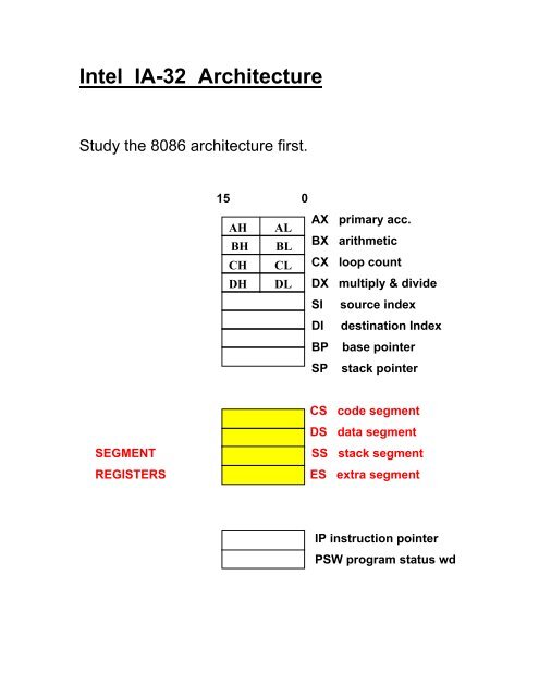
<strong>Intel</strong> <strong>IA</strong>-<strong>32</strong> <strong>Architecture</strong><br />
Study the 8086 architecture first.<br />
15 0<br />
AH AL<br />
BH BL<br />
CH CL<br />
DH DL<br />
AX primary acc.<br />
BX arithmetic<br />
CX loop count<br />
DX multiply & divide<br />
SI source index<br />
DI destination Index<br />
BP base pointer<br />
SP stack pointer<br />
CS code segment<br />
DS data segment<br />
SEGMENT SS stack segment<br />
REGISTERS ES extra segment<br />
IP instruction pointer<br />
PSW program status wd
<strong>Intel</strong> 8086 Addressing Style<br />
0 0 0 0<br />
Segment reg<br />
+<br />
Offset<br />
Generates a 20-bit memory address<br />
Offset<br />
Segment base
Sample Instructions<br />
Accumulator type AX:= AX + BX<br />
AX:= AX + M<br />
String operations Move a char string<br />
(Uses SI and DI)<br />
Starting from 80386, x86 became a true <strong>32</strong>-bit<br />
architecture. Its instruction set broadly defines the<br />
<strong>IA</strong>-<strong>32</strong> architecture.<br />
<strong>Architecture</strong> vs Organization<br />
CPU architecture refers to the programmer’s<br />
view, i.e. primarily the instruction set. The same<br />
architecture can be implemented in many different<br />
ways. True for <strong>IA</strong>-<strong>32</strong> too.
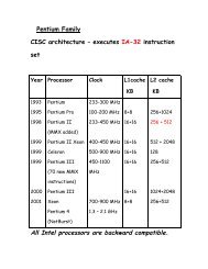
Pentium Family<br />
CISC architecture – executes <strong>IA</strong>-<strong>32</strong> instruction set<br />
Year Processor Clock L1 cache<br />
1993<br />
1995<br />
1998<br />
1999<br />
1999<br />
1999<br />
2000<br />
2001<br />
Pentium<br />
Pentium Pro<br />
Pentium II<br />
(MMX added)<br />
Pentium II Xeon<br />
Celeron<br />
Pentium III<br />
(70 new MMX<br />
instructions)<br />
Pentium III Xeon<br />
Pentium 4<br />
(NetBurst)<br />
60 MHz<br />
100-200 MHz<br />
233-450 MHz<br />
400-450 MHz<br />
500-900 MHz<br />
450-1100 MHz<br />
700-900 MHz<br />
1.3 – 2.1 GHz<br />
KB<br />
8+8<br />
16+16<br />
16+16<br />
16+16<br />
16+16<br />
16+16<br />
8+8<br />
L2 cache<br />
KB<br />
256+1024<br />
256 + 512<br />
512 + 2048<br />
128<br />
256+512<br />
1024+2048<br />
256+512<br />
All <strong>Intel</strong> processors are backward compatible.
<strong>Intel</strong> Pentium Registers<br />
31 16 15 0<br />
EAX<br />
AH AL<br />
AX primary acc.<br />
EBX<br />
BH BL<br />
BX arithmetic<br />
ECX CH CL CX loop count<br />
EDX DH DL<br />
DX mult & div<br />
ESI SI source index<br />
EDI DI dest. Index<br />
EBP BP base pointer<br />
ESP SP stack pointer<br />
CS code segment<br />
DS data segment<br />
SEGMENT SS stack segment<br />
REGISTERS ES extra segment<br />
FS extra segment<br />
GS extra segment<br />
EIP IP instruction pointer<br />
EFLAG PSW program status wd
Pentium Instruction Formats<br />
0-5 1-2 0-1 0-1 0-4 0-4<br />
Prefix opcode mode SIB offset immediate<br />
6 1 1 2 3 3<br />
operation Scale Index Base<br />
byte/word<br />
desitnation 2 3 3<br />
Tells us about the operand<br />
Complex, irregular, and suffers from the legacy of some<br />
bad irreversible design decisions made in the past.<br />
1 st operand = register<br />
MOD REG R/M<br />
Opcode 1 st Operand 2 nd Operand<br />
2 nd Operand = register or memory or immediate
Pentium instruction formats<br />
Two operands: One operand is a Register (REG field), and<br />
the other specified by MOD and R/M.<br />
R/M MOD=00 MOD=01 MOD=10 MOD=11<br />
000 M[EAX] M[EAX+<br />
Offset 8]<br />
001 M[ECX] M[ECX+<br />
Offset 8]<br />
010 M[EDX] M[EDX+<br />
Offset 8]<br />
011 M[EBX] M[EBX+<br />
Offset 8]<br />
100 SIB SIB with<br />
Offset 8<br />
101 Direct M[EBP+<br />
Offset 8]<br />
M[EAX+<br />
Offset <strong>32</strong>]<br />
M[ECX+<br />
Offset <strong>32</strong>]<br />
M[EDX+<br />
Offset <strong>32</strong>]<br />
M[EBX+<br />
Offset <strong>32</strong>]<br />
SIB with<br />
Offset <strong>32</strong><br />
M[EBP+<br />
Offset <strong>32</strong>]<br />
EAX or AL<br />
ECX or CL<br />
EDX or DL<br />
EBX or BL<br />
ESP or AH<br />
EBP or CH<br />
® Using SIB, operand address = Base register + index<br />
register x scale factor (1/2/4) + offset.<br />
® Lack of orthogonality is disturbing
Observations about Pentium Instructions<br />
Variable length instructions: 1 to 17 bytes. It makes the<br />
control unit ugly.<br />
The burden of backward compatibility…<br />
Real mode Runs 8088 programs.<br />
Virtual 8086 mode Runs 8086 programs<br />
Protected mode Works like Pentium<br />
Use of EBP and ESP<br />
ESP<br />
Stack pointer Current stack frame<br />
EBP<br />
Base pointer
What is SIB?<br />
EBP Others (8 bytes)<br />
A[1]<br />
A[2]<br />
A[3]<br />
EAX A[4]<br />
Useful for addressing the elements of an array<br />
Let each element be <strong>32</strong> bits, i.e 4 bytes.<br />
Store the array index i in EAX.<br />
Address of A[i] = EBP + 4*EAX
MMX and SSE instructions<br />
SIMD (Single Instruction Multiple Data) instructions<br />
are useful for multimedia application.<br />
MMX = multimedia<br />
SSE = Streaming SIMD instruction<br />
Supports multimedia operations<br />
Can store 8-bit colors for 8 pixels<br />
in one MMX register and execute<br />
SIMD instructions to accelerate<br />
80 bits<br />
graphics applications FP-cum-MMX<br />
SSE instructions use a separate set of registers.
Prefix bytes<br />
Attributes to instructions…<br />
REP ·instructionÒ<br />
Repeat the instruction until ECX=0<br />
REPZ ·instructionÒ<br />
Repeat the instruction until Z-flag is set.<br />
LOCK ·instructionÒ<br />
Lock the memory bus until the instruction<br />
execution is complete.<br />
Memory<br />
BUS<br />
Processor 1 Processor 2<br />
A multiprocessor