MAX6603 Dual-Channel, Platinum RTD-to-Voltage Signal Conditioner
MAX6603 Dual-Channel, Platinum RTD-to-Voltage Signal Conditioner
MAX6603 Dual-Channel, Platinum RTD-to-Voltage Signal Conditioner

You also want an ePaper? Increase the reach of your titles
YUMPU automatically turns print PDFs into web optimized ePapers that Google loves.
19-3975; Rev 0; 4/06<br />
<strong>Dual</strong>-<strong>Channel</strong>, <strong>Platinum</strong> <strong>RTD</strong>-<strong>to</strong>-<strong>Voltage</strong><br />
<strong>Signal</strong> <strong>Conditioner</strong><br />
General Description<br />
The <strong>MAX6603</strong> dual-channel, platinum <strong>RTD</strong>-<strong>to</strong>-voltage<br />
signal conditioner excites and amplifies the signal from<br />
two external 200Ω platinum-resistive temperature<br />
devices (Pt <strong>RTD</strong>) <strong>to</strong> achieve high-voltage, level-filtered<br />
signals for temperature measurements. The <strong>MAX6603</strong><br />
provides a direct ratiometric output voltage <strong>to</strong> simplify<br />
the interface <strong>to</strong> microcontrollers with integrated analog<strong>to</strong>-digital<br />
converters (ADCs). External precision resis<strong>to</strong>rs<br />
and calibration processes are not needed. The<br />
<strong>MAX6603</strong> provides the necessary signal-conditioning<br />
functions, including ratiometric excitation current,<br />
amplification, buffered voltage outputs, diagnostic fault<br />
detections, and input protection. The <strong>MAX6603</strong> amplifies<br />
signals from two <strong>RTD</strong>s operating over the -40°C <strong>to</strong><br />
+1000°C temperature range and provides the temperature<br />
information as two independent analog voltages.<br />
The <strong>MAX6603</strong> features a ±6°C (max) accuracy over the<br />
+400°C <strong>to</strong> +600°C temperature range.<br />
The <strong>MAX6603</strong> has overvoltage protection up <strong>to</strong> +16V<br />
on <strong>RTD</strong> inputs, and ±5kV electrostatic discharge (ESD)<br />
protection at <strong>RTD</strong> input pins for reliable operation<br />
where <strong>RTD</strong> temperature-sensing probes are used. The<br />
<strong>MAX6603</strong> moni<strong>to</strong>rs the <strong>RTD</strong> for faults and asserts the<br />
respective DG output low for fault conditions. The analog<br />
voltage outputs can be readily connected <strong>to</strong> a variety<br />
of microcontrollers.<br />
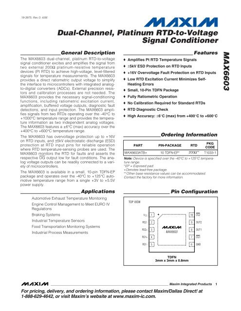
The <strong>MAX6603</strong> is available in a small, 10-pin TDFN-EP<br />
package and operates over the -40°C <strong>to</strong> +125°C au<strong>to</strong>motive<br />
temperature range from a single +3V <strong>to</strong> +5.5V<br />
power supply.<br />
Applications<br />
Au<strong>to</strong>motive Exhaust Temperature Moni<strong>to</strong>ring<br />
Engine Control Management <strong>to</strong> Meet EURO IV<br />
Regulations<br />
Braking Systems<br />
Industrial Temperature Sensors<br />
Food Transportation Moni<strong>to</strong>ring Systems<br />
Industrial Process Measurements<br />
Features<br />
♦ Amplifies Pt <strong>RTD</strong> Temperature <strong>Signal</strong>s<br />
♦ ±5kV ESD Protection on <strong>RTD</strong> Inputs<br />
♦ +16V Overvoltage Fault Protection on <strong>RTD</strong> Inputs<br />
♦ Low <strong>RTD</strong> Excitation Current Minimizes Self-<br />
Heating Errors<br />
♦ Small, 10-Pin TDFN Package<br />
♦ Fully Ratiometric Operation<br />
♦ No Calibration Required for Standard <strong>RTD</strong>s<br />
♦ <strong>RTD</strong> Diagnostic Check<br />
♦ High Accuracy: ±6°C (max) from +400°C <strong>to</strong> +600°C<br />
TOP VIEW<br />
________________________________________________________________ Maxim Integrated Products 1<br />
VCC<br />
RS2-<br />
RS2+<br />
RS1+<br />
RS1-<br />
1<br />
3<br />
4<br />
+<br />
Ordering Information<br />
PART PIN-PACKAGE <strong>RTD</strong><br />
Pin Configuration<br />
2 9 OUT2<br />
<strong>MAX6603</strong><br />
10<br />
8<br />
7<br />
OUT1<br />
5 6 GND<br />
TDFN<br />
3mm x 3mm x 0.8mm<br />
For pricing, delivery, and ordering information, please contact Maxim/Dallas Direct! at<br />
1-888-629-4642, or visit Maxim’s website at www.maxim-ic.com.<br />
DG2<br />
DG1<br />
PKG<br />
CODE<br />
<strong>MAX6603</strong>ATB+ 10 TDFN-EP* 200Ω** T1033-1<br />
Note: Device is specified over the -40°C <strong>to</strong> +125°C temperature<br />
range.<br />
*EP = Exposed pad.<br />
+Denotes lead-free package.<br />
**Other base resistance values can be accommodated.<br />
Contact the fac<strong>to</strong>ry for more information.<br />
<strong>MAX6603</strong>
<strong>MAX6603</strong><br />
<strong>Dual</strong>-<strong>Channel</strong>, <strong>Platinum</strong> <strong>RTD</strong>-<strong>to</strong>-<strong>Voltage</strong><br />
<strong>Signal</strong> <strong>Conditioner</strong><br />
ABSOLUTE MAXIMUM RATINGS<br />
(All voltages referenced <strong>to</strong> GND, unless otherwise noted.)<br />
VCC........................................................................-0.3V <strong>to</strong> +6.0V<br />
RS1+, RS1-, RS2+, RS2- .....................................-0.3V <strong>to</strong> +18.0V<br />
OUT1, OUT2, DG1, DG2 ............................-0.3V <strong>to</strong> (VCC + 0.3V)<br />
Continuous Power Dissipation (TA = +70°C)<br />
10-Pin TDFN Single-Layer Board<br />
(derate 18.5 mW/°C above +70°C).........................1481.5mW<br />
10-Pin TDFN Multilayer Board<br />
(derate 24.4 mW/°C above +70°C).........................1951.2mW<br />
ELECTRICAL CHARACTERISTICS<br />
ESD Protection (OUT1, OUT2, DG1, DG2,<br />
Human Body Model) .....................................................> ±2kV<br />
ESD Protection (RS1+, RS2+, RS1-, RS2-,<br />
VCC, GND, Human Body Model) ..................................> ±5kV<br />
Operating Temperature Range .........................-40°C <strong>to</strong> +125°C<br />
Junction Temperature......................................................+150°C<br />
S<strong>to</strong>rage Temperature Range .............................-65°C <strong>to</strong> +150°C<br />
Lead Temperature (soldering, 10s) .................................+300°C<br />
Stresses beyond those listed under “Absolute Maximum Ratings” may cause permanent damage <strong>to</strong> the device. These are stress ratings only, and functional<br />
operation of the device at these or any other conditions beyond those indicated in the operational sections of the specifications is not implied. Exposure <strong>to</strong><br />
absolute maximum rating conditions for extended periods may affect device reliability.<br />
(VCC = 3.0V <strong>to</strong> 5.5V, resis<strong>to</strong>r connected between RS1+ and RS1- = 560Ω, resis<strong>to</strong>r connected between RS2+ and RS2- = 560Ω,<br />
TA = -40°C <strong>to</strong> +125°C, unless otherwise noted. Typical values are at VCC = 5.0V, RL = 47kΩ between OUT_ and GND, TA = +25°C.)<br />
(Note 1)<br />
PARAMETER SYMBOL CONDITIONS MIN TYP MAX UNITS<br />
Supply <strong>Voltage</strong> VCC 3.0 5.5 V<br />
Input Over <strong>Voltage</strong> VRS RS1+, RS1-, RS2+, RS2- 16 V<br />
Supply Current ICC Sink current during overvoltage fault<br />
VRS1+ = VRS1 - = VRS2+ = VRS2- = +16V<br />
CURRENT SOURCES<br />
2 _______________________________________________________________________________________<br />
3.9 5.5<br />
36.2 47.1<br />
Excitation Current IEXC (Note 2) 0.58 1.0 1.12 mA<br />
Excitation-Current Temperature<br />
Coefficient<br />
TCIEXC (Note 2) -7 ppm/°C<br />
Minimum RS_- <strong>Voltage</strong> VRS_- 3.4 V<br />
Maximum RS_+ <strong>Voltage</strong> VRS_+ 4.0 V<br />
Supply Ratiometric IRATIO VCC = +3V <strong>to</strong> +5.5V 0.2 mA/V<br />
MAXIMUM TEMPERATURE ERROR (Note 3)<br />
<strong>RTD</strong><br />
+400°C <strong>to</strong> +600°C, VCC = 5.0V ±6<br />
-40°C <strong>to</strong> +400°C, VCC = 5.0V ±8<br />
+600°C <strong>to</strong> +1000°C, VCC = 5.0V ±12<br />
+400°C <strong>to</strong> +600°C, VCC = 3.0V ±10<br />
-40°C <strong>to</strong> +400°C, VCC = 3.0V ±13.3<br />
+600°C <strong>to</strong> +1000°C, VCC = 3.0V ±20<br />
mA<br />
°C
<strong>Dual</strong>-<strong>Channel</strong>, <strong>Platinum</strong> <strong>RTD</strong>-<strong>to</strong>-<strong>Voltage</strong><br />
<strong>Signal</strong> <strong>Conditioner</strong><br />
ELECTRICAL CHARACTERISTICS (continued)<br />
(VCC = 3.0V <strong>to</strong> 5.5V, resis<strong>to</strong>r connected between RS1+ and RS1- = 560Ω, resis<strong>to</strong>r connected between RS2+ and RS2- = 560Ω,<br />
TA = -40°C <strong>to</strong> +125°C, unless otherwise noted. Typical values are at VCC = 5.0V, RL = 47kΩ between OUT_ and GND, TA = +25°C.)<br />
(Note 1)<br />
PARAMETER SYMBOL CONDITIONS MIN TYP MAX UNITS<br />
MAXIMUM INPUT RESISTANCE-TO-OUTPUT VOLTAGE ERROR<br />
<strong>RTD</strong> (Note 4)<br />
ANALOG OUTPUTS (OUT1, OUT2)<br />
Output-<strong>Voltage</strong> Low (Max) VOL<br />
Output-<strong>Voltage</strong> High (Min) VOH<br />
Short-Circuit Current ISC<br />
494Ω <strong>to</strong> 627Ω, VCC = 5.0V 19<br />
200Ω <strong>to</strong> 494Ω, VCC = 5.0V 27<br />
627Ω <strong>to</strong> 866Ω, VCC = 5.0V 33<br />
494Ω <strong>to</strong> 627Ω, VCC = 3.0V 19<br />
200Ω <strong>to</strong> 494Ω, VCC = 3.0V 27<br />
627Ω <strong>to</strong> 866Ω, VCC = 3.0V 33<br />
RL = 47kΩ between OUT_ and VCC<br />
(Note 5)<br />
RL = 47kΩ between OUT_ and GND<br />
(Note 5)<br />
Note 1: All parameters are tested at TA = +25°C. Specifications over temperature are guaranteed by design.<br />
Note 2: <strong>RTD</strong> resistance range is 150Ω <strong>to</strong> 900Ω for constant excitation current.<br />
Note 3: A typical 200Ω <strong>RTD</strong>: R(T) = RO[1 + AT + BT 2 ] is referenced for probe temperature-probe resistance relation. The parameters<br />
in this section are not tested and are for reference only.<br />
Note 4: <strong>RTD</strong> resistance is tested only at R<strong>RTD</strong> = 200Ω, 560Ω, 845Ω. The range is guaranteed by design.<br />
Note 5: Parameters are tested in special test mode.<br />
_______________________________________________________________________________________ 3<br />
mV<br />
0.1 V<br />
VCC -<br />
0.1<br />
VOUT = VCC 22 mA<br />
VOUT = GND 12 mA<br />
Maximum Capacitive Load CL 500 pF<br />
Minimum Resistive Load RL Between OUT_ and GND 20 kΩ<br />
DIAGNOSTIC OUTPUTS (DG1, DG2)<br />
Output-<strong>Voltage</strong> Low VOL ISOURCE = 1mA 0.2 V<br />
Output-<strong>Voltage</strong> High VOH ISINK = 1mA<br />
Minimum Resistance for RS+,<br />
RS - Open<br />
Maximum Resistance for RS+,<br />
RS - Short<br />
VCC -<br />
0.2<br />
RRS - OPEN 8000 Ω<br />
RRS - SHORT 60 Ω<br />
V<br />
V<br />
<strong>MAX6603</strong>
<strong>MAX6603</strong><br />
<strong>Dual</strong>-<strong>Channel</strong>, <strong>Platinum</strong> <strong>RTD</strong>-<strong>to</strong>-<strong>Voltage</strong><br />
<strong>Signal</strong> <strong>Conditioner</strong><br />
(VCC = 5.0V, TA = +25°C, unless otherwise noted.)<br />
SUPPLY CURRENT (mA)<br />
PSRR (dB)<br />
3.8<br />
3.5<br />
3.2<br />
2.9<br />
2.6<br />
2.3<br />
SUPPLY CURRENT<br />
vs. SUPPLY VOLTAGE<br />
TA = +25°C<br />
TA = +85°C<br />
TA = +125°C<br />
TA = 0°C<br />
TA = -40°C<br />
2.0<br />
3.0 3.5 4.0 4.5 5.0 5.5<br />
SUPPLY VOLTAGE (V)<br />
POWER-SUPPLY REJECTION RATIO<br />
vs. FREQUENCY<br />
0<br />
-10<br />
-20<br />
-30<br />
-40<br />
-50<br />
-60<br />
-70<br />
-80<br />
-90<br />
-100<br />
0.01 0.10 1.00 10.00 100.00 1000.00<br />
FREQUENCY (kHz)<br />
<strong>MAX6603</strong> <strong>to</strong>c01<br />
<strong>MAX6603</strong> <strong>to</strong>c03<br />
Typical Operating Characteristics<br />
-20<br />
-40 -10 20 50 80 110<br />
TEMPERATURE (°C)<br />
4 _______________________________________________________________________________________<br />
OUTPUT-VOLTAGE DRIFT (mV)<br />
OUTPUT VOLTAGE (V)<br />
20<br />
10<br />
0<br />
-10<br />
5<br />
4<br />
3<br />
2<br />
1<br />
TA = 25°C<br />
OUTPUT-VOLTAGE DRIFT<br />
vs. TEMPERATURE<br />
OUTPUT VOLTAGE<br />
vs. <strong>RTD</strong> RESISTANCE<br />
0<br />
100 300 500 700 900<br />
<strong>RTD</strong> RESISTANCE (Ω)<br />
<strong>MAX6603</strong> <strong>to</strong>c02<br />
<strong>MAX6603</strong> <strong>to</strong>c04
<strong>Dual</strong>-<strong>Channel</strong>, <strong>Platinum</strong> <strong>RTD</strong>-<strong>to</strong>-<strong>Voltage</strong><br />
<strong>Signal</strong> <strong>Conditioner</strong><br />
PIN NAME FUNCTION<br />
RS1+<br />
1 VCC Power-Supply Input. Bypass <strong>to</strong> GND with a 0.1µF capaci<strong>to</strong>r as close <strong>to</strong> VCC as possible.<br />
2 RS2- Sense Resis<strong>to</strong>r 2 Negative Input<br />
3 RS2+ Sense Resis<strong>to</strong>r 2 Positive Input<br />
4 RS1+ Sense Resis<strong>to</strong>r 1 Positive Input<br />
5 RS1- Sense Resis<strong>to</strong>r 1 Negative Input<br />
6 GND Ground<br />
7 DG1 Diagnostic Output <strong>Signal</strong> 1. DG1 asserts low upon fault detection.<br />
8 OUT1 Output Analog <strong>Voltage</strong> 1. OUT1 is high impedance upon DG1 assertion.<br />
9 OUT2 Output Analog <strong>Voltage</strong> 2. OUT2 is high impedance upon DG2 assertion.<br />
10 DG2 Diagnostic Output <strong>Signal</strong> 2. DG2 asserts low upon fault detection.<br />
RS1-<br />
RS2+<br />
— EP Exposed Pad. Connect <strong>to</strong> GND.<br />
RS2-<br />
ESD<br />
CLAMP<br />
ESD<br />
CLAMP<br />
ESD<br />
CLAMP<br />
ESD<br />
CLAMP<br />
Functional Block Diagram<br />
VCC<br />
VCC<br />
RSRC<br />
RSRC<br />
IEXC<br />
IEXC<br />
VCC<br />
HI-V<br />
DETECT<br />
HI-V<br />
DETECT<br />
GND<br />
<strong>MAX6603</strong><br />
AMP<br />
AMP<br />
FAULT<br />
DETECT<br />
FAULT<br />
DETECT<br />
OUT1<br />
DG1<br />
OUT2<br />
DG2<br />
Detailed Description<br />
The <strong>MAX6603</strong> converts a Deutsche Institute for Normung<br />
(DIN) standard 200Ω Pt <strong>RTD</strong> <strong>to</strong> a high-level analog voltage<br />
without the need for external trims or precise discrete<br />
components. The Pt <strong>RTD</strong> resistance conveys<br />
temperature information approximated by the Callendar-<br />
Van Dusen equation and is represented in Figure 1:<br />
R(T) = RO[1 + AT + BT 2 + CT 3 ]<br />
Pin Description<br />
where: R(T) = Resistance of Pt <strong>RTD</strong> at temperature (T)<br />
R0 = Base resistance in ohms at 0°C<br />
T = Temperature in °C<br />
A = 3.9083 E-3 °C-1 (alpha coefficient 1)<br />
B = -5.7750 E-7 °C-2 (alpha coefficient 2)<br />
C = 0 (approximation for temperatures > 0°C)<br />
(Alpha coefficients can vary depending on<br />
standards.)<br />
The <strong>MAX6603</strong> applies a constant excitation current of<br />
1mA (typ) through the Pt <strong>RTD</strong>, generating a voltage<br />
drop that is amplified and results in a high-level output<br />
voltage. The excitation current (IEXC) typically varies<br />
ratiometrically by 0.2mA/V (typ) with respect <strong>to</strong> VCC,<br />
and therefore, the amplified signal is ratiometric <strong>to</strong> the<br />
power supply. The voltage amplification from input <strong>to</strong><br />
output is 5 (typ). The output voltage is applied <strong>to</strong> a<br />
ratiometric ADC <strong>to</strong> produce a digital value independent<br />
of supply voltage. For ADCs that use VCC as their reference<br />
voltage, sudden changes in the supply voltage do<br />
not affect the microcontroller’s reading of the temperature.<br />
Ratiometricity simplifies the connection <strong>to</strong> most<br />
_______________________________________________________________________________________ 5<br />
<strong>MAX6603</strong>
<strong>MAX6603</strong><br />
<strong>Dual</strong>-<strong>Channel</strong>, <strong>Platinum</strong> <strong>RTD</strong>-<strong>to</strong>-<strong>Voltage</strong><br />
<strong>Signal</strong> <strong>Conditioner</strong><br />
microcontrollers that incorporate an ADC and enables a<br />
low-cost, low-complexity solution. Ratiometricity is an<br />
important consideration for battery-operated instruments,<br />
au<strong>to</strong>motive, and some industrial applications.<br />
Temperature Information<br />
The <strong>MAX6603</strong> measures the resistance between the<br />
<strong>RTD</strong> and translates that in<strong>to</strong> a high-level output voltage.<br />
The resistance range of the <strong>MAX6603</strong> is between 150Ω<br />
and 900Ω, covering a -40°C <strong>to</strong> +1000°C temperature<br />
range. When R(T) goes <strong>to</strong>o low or <strong>to</strong>o high, a fault condition<br />
is asserted and the respective DG_ goes low.<br />
Output <strong>Voltage</strong><br />
The following equation describes the output voltage:<br />
where:<br />
RESISTANCE (Ω)<br />
1000<br />
900<br />
800<br />
700<br />
600<br />
500<br />
400<br />
300<br />
200<br />
100<br />
0<br />
200Ω Pt <strong>RTD</strong><br />
0 200 400 600 800 1000<br />
TEMPERATURE (°C)<br />
Figure 1. Typical 200Ω Pt <strong>RTD</strong> Representation by the<br />
Simplified Callender-Van Dusen Equation<br />
V R<br />
V<br />
CC × ( T)<br />
OUT =<br />
1000<br />
VCC = supply voltage<br />
R(T) = <strong>RTD</strong> resistance given by Callendar-<br />
Van Dusen equation.<br />
Using Other Pt <strong>RTD</strong>s<br />
The <strong>MAX6603</strong> is designed for a 200Ω Pt <strong>RTD</strong>, but the<br />
device can work with any <strong>RTD</strong> as long as the resistance<br />
is in the 150Ω <strong>to</strong> 900Ω range. A 500Ω Pt <strong>RTD</strong> can be<br />
used for temperatures up <strong>to</strong> +208°C because that temperature<br />
results in R(T) = 900Ω.<br />
Input Overvoltage Protection <strong>to</strong> +16V<br />
The input pins RS1+, RS1-, RS2+, and RS2- protect the<br />
<strong>MAX6603</strong> from overvoltage conditions up <strong>to</strong> +16V without<br />
damaging the device.<br />
Diagnostic Outputs (DG1, DG2)<br />
The <strong>MAX6603</strong> continuously moni<strong>to</strong>rs the excitation<br />
current <strong>to</strong> the <strong>RTD</strong>, the resultant voltage drop, and<br />
voltage levels of the inputs <strong>to</strong> detect fault conditions.<br />
Any fault condition causes the respective DG output <strong>to</strong><br />
assert low. Fault conditions occur for <strong>RTD</strong> open circuits;<br />
<strong>RTD</strong> short circuits; and RS1+, RS1-, RS2+, and RS2short<br />
<strong>to</strong> ground or supply. If any fault is detected, the<br />
respective DG output asserts low. OUT1 and OUT2 are<br />
high impedance on assertion of DG1 and DG2, respectively.<br />
An example circuit showing potential fault conditions<br />
is shown in Figure 2.<br />
Applications Information<br />
Ratiometric Output Coupled <strong>to</strong> a<br />
Microcontroller<br />
The circuit of Figure 3 shows the <strong>MAX6603</strong> connected <strong>to</strong><br />
the microcontroller using VCC as the ADC reference voltage.<br />
The output is ratiometric <strong>to</strong> VCC, and temperature<br />
measurements are independent of the supply voltage.<br />
PROCESS: BiCMOS<br />
6 _______________________________________________________________________________________<br />
Chip Information
<strong>RTD</strong> SENSOR<br />
OPEN<br />
OPEN<br />
<strong>Dual</strong>-<strong>Channel</strong>, <strong>Platinum</strong> <strong>RTD</strong>-<strong>to</strong>-<strong>Voltage</strong><br />
<strong>Signal</strong> <strong>Conditioner</strong><br />
SHORT TO BAT<br />
(16V)<br />
SHORT TO BAT<br />
(16V)<br />
±5kV ESD<br />
SHORT TO GND<br />
SHORT TO GND<br />
SHORT TOGETHER<br />
CHASSIS GND<br />
RS2+<br />
RS2-<br />
RS1+<br />
RS1-<br />
ESD<br />
CLAMP<br />
ESD<br />
CLAMP<br />
ESD<br />
CLAMP<br />
ESD<br />
CLAMP<br />
VCC<br />
VCC<br />
RSRC<br />
RSRC<br />
0.1µF +5V<br />
0.1µF<br />
<strong>MAX6603</strong><br />
Figure 2. The various fault conditions that cause the diagnostic output <strong>to</strong> assert low are shown for a single channel.<br />
_______________________________________________________________________________________ 7<br />
IEXC<br />
IEXC<br />
VCC<br />
HI-V<br />
DETECT<br />
HI-V<br />
DETECT<br />
GND<br />
AMP<br />
AMP<br />
FAULT<br />
DETECT<br />
FAULT<br />
DETECT<br />
OUT1<br />
DG1<br />
OUT2<br />
DG2<br />
ADC1<br />
INPUT1<br />
ADC2<br />
ADC-REF VCC<br />
MICROCONTROLLER<br />
INPUT2<br />
<strong>MAX6603</strong>
<strong>MAX6603</strong><br />
<strong>Dual</strong>-<strong>Channel</strong>, <strong>Platinum</strong> <strong>RTD</strong>-<strong>to</strong>-<strong>Voltage</strong><br />
<strong>Signal</strong> <strong>Conditioner</strong><br />
Pt <strong>RTD</strong> PROBE<br />
Pt <strong>RTD</strong> PROBE<br />
CONNECTOR<br />
CONNECTOR<br />
<strong>MAX6603</strong><br />
8 _______________________________________________________________________________________<br />
RS1+<br />
RS1-<br />
RS2+<br />
RS2-<br />
ESD<br />
CLAMP<br />
ESD<br />
CLAMP<br />
ESD<br />
CLAMP<br />
ESD<br />
CLAMP<br />
VCC<br />
VCC<br />
RSRC<br />
RSRC<br />
0.1µF +5V<br />
0.1µF<br />
IEXC<br />
IEXC<br />
VCC<br />
HI-V<br />
DETECT<br />
HI-V<br />
DETECT<br />
GND<br />
AMP<br />
AMP<br />
FAULT<br />
DETECT<br />
FAULT<br />
DETECT<br />
Figure 3. A Typical Application Circuit with Ratiometric Output Coupled <strong>to</strong> Ratiometric Microcontroller ADC<br />
OUT1<br />
DG1<br />
OUT2<br />
DG2<br />
ADC1<br />
INPUT1<br />
ADC2<br />
INPUT2<br />
ADC-REF<br />
MICROCONTROLLER
<strong>Dual</strong>-<strong>Channel</strong>, <strong>Platinum</strong> <strong>RTD</strong>-<strong>to</strong>-<strong>Voltage</strong><br />
<strong>Signal</strong> <strong>Conditioner</strong><br />
Package Information<br />
(The package drawing(s) in this data sheet may not reflect the most current specifications. For the latest package outline information,<br />
go <strong>to</strong> www.maxim-ic.com/packages.)<br />
PIN 1<br />
INDEX<br />
AREA<br />
-DRAWING NOT TO SCALE-<br />
D<br />
COMMON DIMENSIONS<br />
SYMBOL MIN. MAX.<br />
A 0.70 0.80<br />
D 2.90 3.10<br />
E 2.90 3.10<br />
A1 0.00 0.05<br />
L 0.20 0.40<br />
k<br />
0.25 MIN.<br />
A2 0.20 REF.<br />
E<br />
A<br />
A1<br />
LC L C<br />
Maxim cannot assume responsibility for use of any circuitry other than circuitry entirely embodied in a Maxim product. No circuit patent licenses are<br />
implied. Maxim reserves the right <strong>to</strong> change the circuitry and specifications without notice at any time.<br />
Maxim Integrated Products, 120 San Gabriel Drive, Sunnyvale, CA 94086 408-737-7600 _____________________ 9<br />
© 2006 Maxim Integrated Products Printed USA is a registered trademark of Maxim Integrated Products, Inc.<br />
A2<br />
DETAIL A<br />
PACKAGE VARIATIONS<br />
PKG. CODE N D2 E2 e JEDEC SPEC b [(N/2)-1] x e<br />
T633-1 6 1.50±0.10 2.30±0.10 0.95 BSC MO229 / WEEA 0.40±0.05 1.90 REF<br />
T633-2 6 1.50±0.10 2.30±0.10 0.95 BSC MO229 / WEEA 0.40±0.05 1.90 REF<br />
T833-1<br />
T1033-1<br />
T1433-1<br />
8<br />
10<br />
14<br />
1.50±0.10<br />
1.50±0.10<br />
2.30±0.10<br />
2.30±0.10<br />
1.70±0.10 2.30±0.10<br />
0.65 BSC<br />
0.50 BSC<br />
0.40 BSC<br />
MO229 / WEEC<br />
- - - -<br />
E2<br />
b<br />
L<br />
N<br />
0.30±0.05<br />
0.25±0.05<br />
0.20±0.05<br />
e<br />
1.95 REF<br />
T833-2 8 1.50±0.10 2.30±0.10 0.65 BSC MO229 / WEEC 0.30±0.05 1.95 REF<br />
T833-3 8 1.50±0.10 2.30±0.10 0.65 BSC MO229 / WEEC 0.30±0.05 1.95 REF<br />
T1433-2 14 1.70±0.10 2.30±0.10<br />
MO229 / WEED-3<br />
2.00 REF<br />
2.40 REF<br />
0.40 BSC - - - - 0.20±0.05 2.40 REF<br />
D2<br />
0.35x0.35<br />
k<br />
PACKAGE OUTLINE, 6,8,10 & 14L,<br />
TDFN, EXPOSED PAD, 3x3x0.80 mm<br />
DOWNBONDS<br />
ALLOWED<br />
NO<br />
NO<br />
NO<br />
NO<br />
YES<br />
NO<br />
YES<br />
NO<br />
e<br />
21-0137<br />
PIN 1 ID<br />
PACKAGE OUTLINE, 6,8,10 & 14L,<br />
TDFN, EXPOSED PAD, 3x3x0.80 mm<br />
e<br />
[(N/2)-1] x e<br />
REF.<br />
-DRAWING NOT TO SCALE- G 2 21-0137<br />
2<br />
L<br />
G 1 2<br />
6, 8, &10L, DFN THIN.EPS<br />
<strong>MAX6603</strong>