ispLSI 2032E Data Sheet - Lattice Semiconductor
ispLSI 2032E Data Sheet - Lattice Semiconductor
ispLSI 2032E Data Sheet - Lattice Semiconductor

You also want an ePaper? Increase the reach of your titles
YUMPU automatically turns print PDFs into web optimized ePapers that Google loves.
Features<br />
• SuperFAST HIGH DENSITY IN-SYSTEM<br />
PROGRAMMABLE LOGIC<br />
— 1000 PLD Gates<br />
— 32 I/O Pins, Two Dedicated Inputs<br />
— 32 Registers<br />
— High Speed Global Interconnect<br />
— Wide Input Gating for Fast Counters, State<br />
Machines, Address Decoders, etc.<br />
— Small Logic Block Size for Random Logic<br />
— 100% Functionally and JEDEC Upward Compatible<br />
with <strong>ispLSI</strong> 2032 Devices<br />
• HIGH PERFORMANCE E2CMOS ® TECHNOLOGY<br />
— fmax = 225 MHz Maximum Operating Frequency<br />
— tpd = 3.5 ns Propagation Delay<br />
— TTL Compatible Inputs and Outputs<br />
— 5V Programmable Logic Core<br />
— ispJTAG In-System Programmable via IEEE 1149.1<br />
(JTAG) Test Access Port<br />
— User-Selectable 3.3V or 5V I/O (48-Pin Package Only)<br />
Supports Mixed Voltage Systems<br />
— PCI Compatible Outputs (48-Pin Package Only)<br />
— Open-Drain Output Option<br />
— Electrically Erasable and Reprogrammable<br />
— Non-Volatile<br />
— Unused Product Term Shutdown Saves Power<br />
• <strong>ispLSI</strong> OFFERS THE FOLLOWING ADDED FEATURES<br />
— Increased Manufacturing Yields, Reduced Time-to-<br />
Market and Improved Product Quality<br />
— Reprogram Soldered Devices for Faster Prototyping<br />
• OFFERS THE EASE OF USE AND FAST SYSTEM<br />
SPEED OF PLDs WITH THE DENSITY AND FLEXIBILITY<br />
OF FIELD PROGRAMMABLE GATE ARRAYS<br />
— Complete Programmable Device Can Combine Glue<br />
Logic and Structured Designs<br />
— Enhanced Pin Locking Capability<br />
— Three Dedicated Clock Input Pins<br />
— Synchronous and Asynchronous Clocks<br />
— Programmable Output Slew Rate Control to<br />
Minimize Switching Noise<br />
— Flexible Pin Placement<br />
— Optimized Global Routing Pool Provides Global<br />
Interconnectivity<br />
LATTICE SEMICONDUCTOR CORP., 5555 Northeast Moore Ct., Hillsboro, Oregon 97124, U.S.A.<br />
Tel. (503) 268-8000; 1-800-LATTICE; FAX (503) 268-8556; http://www.latticesemi.com<br />
2032e_05 1<br />
<strong>ispLSI</strong> ®<br />
<strong>2032E</strong><br />
In-System Programmable<br />
SuperFAST High Density PLD<br />
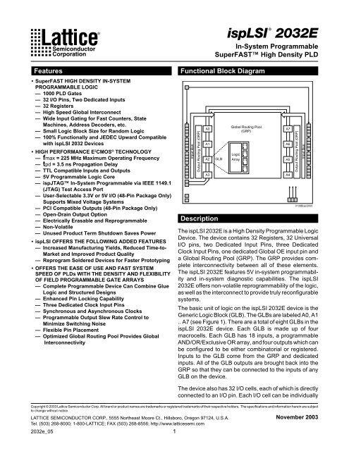
Functional Block Diagram<br />
Global Routing Pool<br />
(GRP)<br />
Copyright © 2003 <strong>Lattice</strong> <strong>Semiconductor</strong> Corp. All brand or product names are trademarks or registered trademarks of their respective holders. The specifications and information herein are subject<br />
to change without notice.<br />
Input Bus<br />
Output Routing Pool (ORP)<br />
A0<br />
A1<br />
A2 GLB<br />
A3<br />
Description<br />
Logic<br />
Array<br />
D Q<br />
D Q<br />
D Q<br />
D Q<br />
A7<br />
A6<br />
A5<br />
A4<br />
Output Routing Pool (ORP)<br />
Input Bus<br />
0139Bisp/2000<br />
The <strong>ispLSI</strong> <strong>2032E</strong> is a High Density Programmable Logic<br />
Device. The device contains 32 Registers, 32 Universal<br />
I/O pins, two Dedicated Input Pins, three Dedicated<br />
Clock Input Pins, one dedicated Global OE input pin and<br />
a Global Routing Pool (GRP). The GRP provides complete<br />
interconnectivity between all of these elements.<br />
The <strong>ispLSI</strong> <strong>2032E</strong> features 5V in-system programmability<br />
and in-system diagnostic capabilities. The <strong>ispLSI</strong><br />
<strong>2032E</strong> offers non-volatile reprogrammability of the logic,<br />
as well as the interconnect to provide truly reconfigurable<br />
systems.<br />
The basic unit of logic on the <strong>ispLSI</strong> <strong>2032E</strong> device is the<br />
Generic Logic Block (GLB). The GLBs are labeled A0, A1<br />
.. A7 (see Figure 1). There are a total of eight GLBs in the<br />
<strong>ispLSI</strong> <strong>2032E</strong> device. Each GLB is made up of four<br />
macrocells. Each GLB has 18 inputs, a programmable<br />
AND/OR/Exclusive OR array, and four outputs which can<br />
be configured to be either combinatorial or registered.<br />
Inputs to the GLB come from the GRP and dedicated<br />
inputs. All of the GLB outputs are brought back into the<br />
GRP so that they can be connected to the inputs of any<br />
GLB on the device.<br />
The device also has 32 I/O cells, each of which is directly<br />
connected to an I/O pin. Each I/O cell can be individually<br />
November 2003
Functional Block Diagram<br />
Figure 1. <strong>ispLSI</strong> <strong>2032E</strong> Functional Block Diagram<br />
GOE 0<br />
I/O 0<br />
I/O 1<br />
I/O 2<br />
I/O 3<br />
I/O 4<br />
I/O 5<br />
I/O 6<br />
I/O 7<br />
I/O 8<br />
I/O 9<br />
I/O 10<br />
I/O 11<br />
I/O 12<br />
I/O 13<br />
I/O 14<br />
I/O 15<br />
TDI/IN 0<br />
TDO/IN 1<br />
TMS<br />
BSCAN<br />
Input Bus<br />
Output Routing Pool (ORP)<br />
A0<br />
A1<br />
A2<br />
A3<br />
Notes:<br />
*Y1 and RESET are multiplexed on the same pin<br />
programmed to be a combinatorial input, output or bidirectional<br />
I/O pin with 3-state control. The signal levels<br />
are TTL compatible voltages and the output drivers can<br />
source 4 mA or sink 8 mA. Each output can be programmed<br />
independently for fast or slow output slew rate<br />
to minimize overall output switching noise. By connecting<br />
the VCCIO pins to a common 5V or 3.3V power supply,<br />
I/O output levels can be matched to 5V or 3.3V compatible<br />
voltages. When connected to a 5V supply, the I/O<br />
pins provide PCI-compatible output drive (48-pin device<br />
only).<br />
Eight GLBs, 32 I/O cells, two dedicated inputs and two<br />
ORPs are connected together to make a Megablock (see<br />
Figure 1). The outputs of the eight GLBs are connected<br />
to a set of 32 universal I/O cells by the ORP. Each <strong>ispLSI</strong><br />
<strong>2032E</strong> device contains one Megablock.<br />
The GRP has as its inputs, the outputs from all of the<br />
GLBs and all of the inputs from the bi-directional I/O cells.<br />
All of these signals are made available to the inputs of the<br />
GLBs. Delays through the GRP have been equalized to<br />
minimize timing skew.<br />
Global Routing Pool<br />
(GRP)<br />
2<br />
Specifications <strong>ispLSI</strong> <strong>2032E</strong><br />
Y0<br />
Y1*<br />
TCK/Y2<br />
A7<br />
A6<br />
A5<br />
A4<br />
CLK 0<br />
CLK 1<br />
CLK 2<br />
Output Routing Pool (ORP)<br />
Input Bus<br />
I/O 31<br />
I/O 30<br />
I/O 29<br />
I/O 28<br />
I/O 27<br />
I/O 26<br />
I/O 25<br />
I/O 24<br />
I/O 23<br />
I/O 22<br />
I/O 21<br />
I/O 20<br />
I/O 19<br />
I/O 18<br />
I/O 17<br />
I/O 16<br />
0139/<strong>2032E</strong><br />
Clocks in the <strong>ispLSI</strong> <strong>2032E</strong> device are selected using the<br />
dedicated clock pins. Three dedicated clock pins (Y0, Y1,<br />
Y2) or an asynchronous clock can be selected on a GLB<br />
basis. The asynchronous or Product Term clock can be<br />
generated in any GLB for its own clock.<br />
Programmable Open-Drain Outputs<br />
In addition to the standard output configuration, the<br />
outputs of the <strong>ispLSI</strong> <strong>2032E</strong> are individually programmable,<br />
either as a standard totem-pole output or an<br />
open-drain output. The totem-pole output drives the<br />
specified Voh and Vol levels, whereas the open-drain<br />
output drives only the specified Vol. The Voh level on the<br />
open-drain output depends on the external loading and<br />
pull-up. This output configuration is controlled by a programmable<br />
fuse. The default configuration when the<br />
device is in bulk erased state is totem-pole configuration.<br />
The open-drain/totem-pole option is selectable through<br />
the <strong>Lattice</strong> software tools.
Absolute Maximum Ratings 1<br />
Supply Voltage V cc .................................. -0.5 to +7.0V<br />
Input Voltage Applied........................ -2.5 to V CC +1.0V<br />
Off-State Output Voltage Applied ..... -2.5 to V CC +1.0V<br />
Storage Temperature ................................ -65 to 150°C<br />
Case Temp. with Power Applied .............. -55 to 125°C<br />
Max. Junction Temp. (T J) with Power Applied ... 150°C<br />
3<br />
Specifications <strong>ispLSI</strong> <strong>2032E</strong><br />
1. Stresses above those listed under the “Absolute Maximum Ratings” may cause permanent damage to the device. Functional<br />
operation of the device at these or at any other conditions above those indicated in the operational sections of this specification<br />
is not implied (while programming, follow the programming specifications).<br />
DC Recommended Operating Condition<br />
VCC<br />
VCCIO 1<br />
VIL<br />
VIH<br />
SYMBOL<br />
Input Low Voltage<br />
Input High Voltage<br />
1. 3.3V I/O operation not available for 44-pin packages.<br />
Capacitance (T A=25°C, f=1.0 MHz)<br />
PARAMETER<br />
Supply Voltage: Logic Core, Input Buffers<br />
5V<br />
Supply Voltage: Output Drivers<br />
3.3V<br />
T A = 0°C to +70°C<br />
MIN. MAX. UNITS<br />
4.75 5.25 V<br />
SYMBOL<br />
PARAMETER<br />
TYP UNITS TEST CONDITIONS<br />
C1<br />
Dedicated Input Capacitance<br />
6 pf V CC=<br />
5.0V, V IN = 2.0V<br />
C2<br />
I/O Capacitance<br />
7 pf V CC= 5.0V, V I/O = 2.0V<br />
C3 Clock Capacitance<br />
10 pf V CC= 5.0V, V Y=<br />
2.0V<br />
Erase/Reprogram Specification<br />
4.75 5.25 V<br />
3.0 3.6 V<br />
PARAMETER MINIMUM MAXIMUM UNITS<br />
Erase/Reprogram Cycles 10,000 – Cycles<br />
0<br />
2.0<br />
0.8<br />
V cc+1<br />
V<br />
V<br />
Table 2-0005/<strong>2032E</strong><br />
Table 2-0006/<strong>2032E</strong><br />
Table 2-0008/<strong>2032E</strong>
Switching Test Conditions<br />
Input Pulse Levels<br />
Input Rise and Fall Time 10% to 90%<br />
Input Timing Reference Levels<br />
Output Timing Reference Levels<br />
Output Load<br />
3-state levels are measured 0.5V from<br />
steady-state active level.<br />
Output Load Conditions (see Figure 2)<br />
GND to 3.0V<br />
1.5 ns<br />
1.5V<br />
1.5V<br />
See Figure 2<br />
Table 2-0003/<strong>2032E</strong><br />
TEST CONDITION R1 R2 CL<br />
A 470Ω 390Ω 35pF<br />
B<br />
Active High<br />
Active Low<br />
∞<br />
470Ω<br />
390Ω<br />
390Ω<br />
35pF<br />
35pF<br />
C<br />
Active High to Z<br />
at V OH-0.5V<br />
Active Low to Z<br />
at V OL+0.5V<br />
∞<br />
470Ω<br />
390Ω<br />
390Ω<br />
5pF<br />
5pF<br />
Table 2 - 0004A<br />
4<br />
Specifications <strong>ispLSI</strong> <strong>2032E</strong><br />
Figure 2. Test Load<br />
Device<br />
Output<br />
DC Electrical Characteristics<br />
Over Recommended Operating Conditions1 + 5V<br />
R1<br />
R2<br />
CL*<br />
*CL includes Test Fixture and Probe Capacitance.<br />
SYMBOL<br />
PARAMETER<br />
VOL<br />
VOH<br />
IIL<br />
IIH<br />
IIL-PU<br />
IOS<br />
Table 2-0007/<strong>2032E</strong><br />
1. One output at a time for a maximum duration of one second (VOUT = 0.5V). Characterized, but not 100% tested.<br />
2. Meaured using two 16-bit counters.<br />
3. Typical values are at VCC = 5V and TA = 25°C.<br />
4. Unused inputs held at 0.0V.<br />
5. Available in 48-pin package only.<br />
6. Maximum ICC varies widely with specific device configuration and operating frequency. Refer to the<br />
Power Consumption section of this data sheet and the Thermal Management section of the <strong>Lattice</strong> <strong>Semiconductor</strong><br />
<strong>Data</strong> Book or CD-ROM to estimate maximum ICC.<br />
1<br />
ICC 2,4,6<br />
CONDITION MIN. TYP.<br />
Output Low Voltage<br />
IOL = 8 mA<br />
Output High Voltage<br />
IOH = -4 mA<br />
Input or I/O Low Leakage Current 0V ≤ VIN ≤ VIL (Max.)<br />
I/O Active Pull-Up Current, non-PCI 0V ≤ VIN ≤ 2.0V<br />
Output Short Circuit Current, non-PCI VCCIO = 5V, VOUT = 0.5V<br />
Operating Power Supply Current<br />
VIL = 0.0V, VIH = 3.0V<br />
3 MAX. UNITS<br />
– – 0.4 V<br />
2.4 – – V<br />
– – -10 µA<br />
Input or I/O High Leakage Current<br />
(VCCIO - 0.2)V ≤ VIN ≤ VCCIO VCCIO ≤ VIN ≤ 5.25V<br />
–<br />
–<br />
–<br />
–<br />
10<br />
10<br />
µA<br />
µA<br />
I/O Active Pull-Up Current, PCI<br />
-10 – -150 µA<br />
– – -200<br />
5<br />
0V ≤ VIN ≤ 2.0V -10 – -250 µA<br />
mA<br />
Output Short Circuit Current, PCI 5<br />
VCCIO = 5.0V or 3.3V, VOUT = 0.5V – – -240 mA<br />
fTOGGLE = 1 MHz<br />
-225/-200<br />
Others<br />
–<br />
–<br />
85<br />
65<br />
–<br />
–<br />
mA<br />
mA<br />
Test<br />
Point<br />
0213A
External Timing Parameters<br />
Over Recommended Operating Conditions<br />
5<br />
Specifications <strong>ispLSI</strong> <strong>2032E</strong><br />
TEST<br />
COND.<br />
#<br />
1<br />
DESCRIPTION<br />
-200<br />
MIN. MAX.<br />
-180<br />
MIN. MAX.<br />
UNITS<br />
tpd1<br />
1<br />
( tsu2 + tco1)<br />
1. Unless noted otherwise, all parameters use a GRP load of four GLBs, 20 PTXOR path, ORP and Y0 clock.<br />
2. Refer to Timing Model in this data sheet for further details.<br />
3. Standard 16-bit counter using GRP feedback.<br />
4. Reference Switching Test Conditions section.<br />
2<br />
PARAMETER<br />
4<br />
A 1 <strong>Data</strong> Prop. Delay, 4PT Bypass, ORP Bypass – 3.5 – 5.0 ns<br />
tpd2 A 2 <strong>Data</strong> Prop. Delay – – ns<br />
fmax A 3 Clk Frequency with Int. Feedback3 -225<br />
MIN. MAX.<br />
– 3.5<br />
– 5.5 5.5 7.5<br />
225 – 200 – 180 – MHz<br />
fmax (Ext.) – 4 Clk Frequency with Ext. Feedback 167 – 167 – 125 – MHz<br />
fmax (Tog.) – 5 Clk Frequency, Max. Toggle 250 – 250 – 200 – MHz<br />
tsu1 – 6 GLB Reg. Setup Time before Clk, 4 PT Bypass 2.5 – 2.5 – 3.0 – ns<br />
tco1 A 7 GLB Reg. Clk to Output Delay, ORP Bypass – 2.5 – 2.5 – 4.0 ns<br />
th1 – 8 GLB Reg. Hold Time after Clk, 4 PT Bypass 0.0 – 0.0 – 0.0 – ns<br />
tsu2 – 9 GLB Reg. Setup Time before Clk 3.5 – 3.5 – 4.0 – ns<br />
tco2 – 10 GLB Reg. Clk to Output Delay – 3.5 – 3.5 – 4.5 ns<br />
th2 – 11 GLB Reg. Hold Time after Clk 0.0 – 0.0 – 0.0 – ns<br />
tr1 A 12 Ext. Reset Pin to Output Delay, ORP Bypass – 5.0 – 5.0 – 6.5 ns<br />
trw1 – 13 Ext. Reset Pulse Duration 3.5 – 3.5 – 4.0 – ns<br />
tptoeen B 14 Input to Output Enable – 7.0 – 7.0 – 10.0 ns<br />
tptoedis C 15 Input to Output Disable – 7.0 – 7.0 – 10.0 ns<br />
tgoeen B 16 Global OE Output Enable – 3.5 – 3.5 – 5.0 ns<br />
tgoedis C 17 Global OE Output Disable – 3.5 – 3.5 – 5.0<br />
ns<br />
twh – 18 Ext. Synch. Clk Pulse Duration, High 2.0 – 2.0 – 2.5 – ns<br />
twl – 19 Ext. Synch. Clk Pulse Duration, Low 2.0 – 2.0 – 2.5 – ns<br />
USE <strong>2032E</strong>-225 FOR<br />
NEW DESIGNS<br />
Table 2-0030A/<strong>2032E</strong>
External Timing Parameters<br />
Over Recommended Operating Conditions<br />
6<br />
Specifications <strong>ispLSI</strong> <strong>2032E</strong><br />
TEST<br />
COND.<br />
#<br />
1<br />
DESCRIPTION<br />
-135<br />
MIN. MAX.<br />
-110<br />
MIN. MAX.<br />
UNITS<br />
tpd1<br />
1<br />
( tsu2 + tco1)<br />
1. Unless noted otherwise, all parameters use a GRP load of four GLBs, 20 PTXOR path, ORP and Y0 clock.<br />
2. Refer to Timing Model in this data sheet for further details.<br />
3. Standard 16-bit counter using GRP feedback.<br />
4. Reference Switching Test Conditions section.<br />
2<br />
PARAMETER<br />
4<br />
A 1 <strong>Data</strong> Propagation Delay, 4PT Bypass, ORP Bypass – 7.5 – 10.0 ns<br />
tpd2 A 2 <strong>Data</strong> Propagation Delay – – ns<br />
fmax A 3 Clock Frequency with Internal Feedback3 10.0 13.0<br />
137 – 111 – MHz<br />
fmax (Ext.) – 4 Clock Frequency with External Feedback 100 – 77.0 – MHz<br />
fmax (Tog.) – 5 Clock Frequency, Max. Toggle 167 – 125 – MHz<br />
tsu1 – 6 GLB Register Setup Time before Clock, 4 PT Bypass 4.0 – 5.5 – ns<br />
tco1 A 7 GLB Register Clock to Output Delay, ORP Bypass – 4.5 – 5.5 ns<br />
th1 – 8 GLB Register Hold Time after Clock, 4 PT Bypass 0.0 – 0.0 – ns<br />
tsu2 – 9 GLB Register Setup Time before Clock 5.5 – 7.5 – ns<br />
tco2 – 10 GLB Register Clock to Output Delay – 5.5 – 6.5 ns<br />
th2 – 11 GLB Register Hold Time after Clock 0.0 – 0.0 – ns<br />
tr1 A 12 External Reset Pin to Output Delay, ORP Bypass – 9.0 – 12.5 ns<br />
trw1 – 13 External Reset Pulse Duration 5.0 – 6.5 – ns<br />
tptoeen B 14 Input to Output Enable – 12.0 – 14.5 ns<br />
tptoedis C 15 Input to Output Disable – 12.0 – 14.5 ns<br />
tgoeen B 16 Global OE Output Enable – 6.0 – 7.0 ns<br />
tgoedis C 17 Global OE Output Disable – 6.0 – 7.0<br />
ns<br />
twh – 18 External Synchronous Clock Pulse Duration, High 3.0 – 4.0 – ns<br />
twl – 19 External Synchronous Clock Pulse Duration, Low 3.0 – 4.0 – ns<br />
Table 2-0030B/<strong>2032E</strong>
Internal Timing Parameters 1<br />
Over Recommended Operating Conditions<br />
1. Internal Timing Parameters are not tested and are for reference only.<br />
2. Refer to Timing Model in this data sheet for further details.<br />
3. The XOR adjacent path can only be used by hard macros.<br />
7<br />
Specifications <strong>ispLSI</strong> <strong>2032E</strong><br />
Inputs<br />
# DESCRIPTION<br />
-200<br />
MIN. MAX.<br />
-180<br />
MIN. MAX.<br />
UNITS<br />
tio<br />
2<br />
PARAMETER<br />
-225<br />
MIN. MAX.<br />
20 Input Buffer Delay – 0.6 – 0.4 – 0.6 ns<br />
tdin<br />
GRP<br />
21 Dedicated Input Delay – 1.3 – 1.3 – 1.3 ns<br />
tgrp<br />
GLB<br />
22 GRP Delay – 0.7 – 0.7 – 0.7 ns<br />
t4ptbpc 23 4 Product Term Bypass Path Delay (Combinatorial) – 1.2 – 1.8 – 1.8 ns<br />
t4ptbpr 24 4 Product Term Bypass Path Delay (Registered) – 1.2 – 1.8 – 2.8 ns<br />
t1ptxor 25 1 Product Term/XOR Path Delay – 2.2 – 2.8 – 3.8 ns<br />
t20ptxor 26 20 Product Term/XOR Path Delay – 2.2 – 2.8 – 3.8 ns<br />
txoradj 27 3<br />
XOR Adjacent Path Delay – 2.2 – 2.8 – 3.8 ns<br />
tgbp 28 GLB Register Bypass Delay – 0.0 – 0.0 – 0.0 ns<br />
tgsu 29 GLB Register Setup Time before Clock 0.8 – 0.8 – 0.3 – ns<br />
tgh 30 GLB Register Hold Time after Clock 1.7 – 1.7 – 2.7 – ns<br />
tgco 31 GLB Register Clock to Output Delay – 0.7 – 0.7 – 0.7 ns<br />
tgro 32 GLB Register Reset to Output Delay – 1.3 – 2.9 – 1.1 ns<br />
tptre 33 GLB Product Term Reset to Register Delay – 2.5 – 2.5 – 2.9 ns<br />
tptoe 34 GLB Product Term Output Enable to I/O Cell Delay – 4.2 – 4.4 – 5.9 ns<br />
tptck<br />
ORP<br />
35 GLB Product Term Clock Delay 0.3 2.8 0.7 3.2 1.5 3.7 ns<br />
torp 36 ORP Delay – 1.0 – 1.0 – 1.1 ns<br />
torpbp<br />
Outputs<br />
37 ORP Bypass Delay – 0.0 – 0.0 – 0.6 ns<br />
tob 38 Output Buffer Delay – 1.0 – 0.6 – 1.3 ns<br />
tsl 39 Output Slew Limited Delay Adder – 1.5 – 1.5 – 1.5 ns<br />
toen 40 I/O Cell OE to Output Enabled – 1.5 – 1.5 – 2.8 ns<br />
todis 41 I/O Cell OE to Output Disabled – 1.5 – 1.5 – 2.8 ns<br />
tgoe<br />
Clocks<br />
42 Global Output Enable – 2.0 – 2.0 – 2.2 ns<br />
tgy0 43 Clock Delay, Y0 to Global GLB Clock Line (Ref. clock) 0.8 0.8 1.2 1.2 1.4 1.4 ns<br />
tgy1/2<br />
Global Reset<br />
44 Clock Delay, Y1 or Y2 to Global GLB Clock Line 1.0 1.0 1.4 1.4 1.6 1.6 ns<br />
tgr 45 Global Reset to GLB – 2.7<br />
– 2.7 – 3.5 ns<br />
USE <strong>2032E</strong>-225 FOR NEW DESIGNS<br />
Table 2-0036A/<strong>2032E</strong>
Internal Timing Parameters 1<br />
PARAMETER<br />
Inputs<br />
# 2<br />
DESCRIPTION<br />
8<br />
Specifications <strong>ispLSI</strong> <strong>2032E</strong><br />
-135 -110<br />
UNITS<br />
MIN. MAX. MIN. MAX.<br />
tio<br />
20 Input Buffer Delay – 1.1 – 1.7 ns<br />
tdin<br />
GRP<br />
21 Dedicated Input Delay – 2.4 – 3.4 ns<br />
tgrp 22 GRP Delay – 1.3 – 1.7 ns<br />
GLB<br />
t4ptbpc 23 4 Product Term Bypass Path Delay (Combinatorial) – 3.6 – 4.9 ns<br />
t4ptbpr 24 4 Product Term Bypass Path Delay (Registered) – 3.6 – 4.8 ns<br />
t1ptxor 25 1 Product Term/XOR Path Delay – 5.0 – 6.2 ns<br />
t20ptxor 26 20 Product Term/XOR Path Delay – 5.1 – 6.8 ns<br />
txoradj 27 3<br />
XOR Adjacent Path Delay – 5.6 – 7.5 ns<br />
tgbp 28 GLB Register Bypass Delay – 0.0 – 0.1 ns<br />
tgsu 29 GLB Register Setup Time before Clock 0.3 – 0.5 – ns<br />
tgh 30 GLB Register Hold Time after Clock 3.0 – 4.0 – ns<br />
tgco 31 GLB Register Clock to Output Delay – 0.7 – 0.6 ns<br />
tgro 32 GLB Register Reset to Output Delay – 1.1 – 1.8 ns<br />
tptre 33 GLB Product Term Reset to Register Delay – 4.4 – 5.9 ns<br />
tptoe 34 GLB Product Term Output Enable to I/O Cell Delay – 6.4 – 7.1 ns<br />
tptck<br />
ORP<br />
35 GLB Product Term Clock Delay 2.9 5.2 4.0 7.0 ns<br />
torp 36 ORP Delay – 1.3 – 1.5 ns<br />
torpbp<br />
Outputs<br />
37 ORP Bypass Delay – 0.3 – 0.5 ns<br />
tob 38 Output Buffer Delay – 1.2 – 1.2 ns<br />
tsl 39 Output Slew Limited Delay Adder – 10.0 – 10.0 ns<br />
toen 40 I/O Cell OE to Output Enabled – 3.2 – 4.0 ns<br />
todis 41 I/O Cell OE to Output Disabled – 3.2 – 4.0 ns<br />
tgoe 42 Global Output Enable – 2.8 – 3.0 ns<br />
Clocks<br />
tgy0 43 Clock Delay, Y0 to Global GLB Clock Line (Ref. clock) 2.3 2.3 3.2 3.2 ns<br />
tgy1/2 44 Clock Delay, Y1 or Y2 to Global GLB Clock Line 2.3 2.3 3.2 3.2 ns<br />
Global Reset<br />
tgr 45 Global Reset to GLB – 6.4<br />
– 9.0 ns<br />
1. Internal Timing Parameters are not tested and are for reference only.<br />
2. Refer to Timing Model in this data sheet for further details.<br />
3. The XOR adjacent path can only be used by hard macros.<br />
Table 2-0036B/<strong>2032E</strong>
<strong>ispLSI</strong> <strong>2032E</strong> Timing Model<br />
Ded. In<br />
I/O Pin<br />
(Input)<br />
Reset<br />
Y0,1,2<br />
GOE 0<br />
#21<br />
I/O Cell<br />
Feedback<br />
Derivations of tsu, th and tco from the Product Term Clock<br />
tsu = Logic + Reg su - Clock (min)<br />
= (tio + tgrp + t20ptxor) + (tgsu) - (tio + tgrp + tptck(min))<br />
= (#20 + #22 + #26) + (#29) - (#20 + #22 + #35)<br />
2.7 = (0.6 + 0.7 + 2.2) + (0.8) - (0.6 + 0.7 + 0.3)<br />
th = Clock (max) + Reg h - Logic<br />
= (tio + tgrp + tptck(max)) + (tgh) - (tio + tgrp + t20ptxor)<br />
= (#20 + #22 + #35) + (#30) - (#20 + #22 + #26)<br />
2.3 = (0.6 + 0.7 + 2.8) + (1.7) - (0.6 + 0.7 + 2.2)<br />
tco = Clock (max) + Reg co + Output<br />
= (tio + tgrp + tptck(max)) + (tgco) + (torp + tob)<br />
= (#20 + #22 + #35) + (#31) + (#36 + #38)<br />
6.8 = (0.6 + 0.7 + 2.8) + (0.7) + (1.0 + 1.0)<br />
GRP<br />
Note: Calculations are based upon timing specifications for the <strong>ispLSI</strong> <strong>2032E</strong>-225L<br />
9<br />
Specifications <strong>ispLSI</strong> <strong>2032E</strong><br />
I/O Delay<br />
GRP Reg 4 PT Bypass GLB Reg Bypass ORP Bypass<br />
#20 #22<br />
#24<br />
#28<br />
#37<br />
#45<br />
#43, 44<br />
#42<br />
20 PT<br />
XOR Delays<br />
#25, 26, 27<br />
Control<br />
PTs<br />
#33, 34,<br />
35<br />
RE<br />
OE<br />
CK<br />
GLB<br />
Comb 4 PT Bypass #23<br />
GLB Reg<br />
Delay<br />
D Q<br />
RST<br />
#29, 30,<br />
31, 32<br />
Table 2-0042/<strong>2032E</strong><br />
ORP<br />
ORP<br />
Delay<br />
#36<br />
#38,<br />
#39<br />
#40, 41<br />
0491/<strong>2032E</strong><br />
I/O Cell<br />
I/O Pin<br />
(Output)
Power Consumption<br />
Power consumption in the <strong>ispLSI</strong> <strong>2032E</strong> device depends<br />
on two primary factors: the speed at which the device is<br />
operating and the number of Product Terms used.<br />
Figure 3. Typical Device Power Consumption vs fmax<br />
ICC (mA)<br />
150<br />
140<br />
130<br />
120<br />
110<br />
100<br />
90<br />
80<br />
70<br />
60<br />
50<br />
40<br />
I CC can be estimated for the <strong>ispLSI</strong> <strong>2032E</strong> using the following equation:<br />
10<br />
Specifications <strong>ispLSI</strong> <strong>2032E</strong><br />
Figure 3 shows the relationship between power and<br />
operating speed.<br />
1 20 40 60 80 100 120 140 160 180 200 220 240<br />
fmax (MHz)<br />
Notes: Configuration of two 16-bit counters<br />
Typical current at 5V, 25°C<br />
For <strong>2032E</strong>-225 and -200: ICC = 4.5 + (# of PTs * 1.3) + (# of nets * Max freq * 0.0035)<br />
For <strong>2032E</strong>-180 and Slower: ICC = 4.5 + (# of PTs * 1.02) + (# of nets * Max freq * 0.0035)<br />
Where:<br />
# of PTs = Number of Product Terms used in design<br />
# of nets = Number of Signals used in device<br />
Max freq = Highest Clock Frequency to the device (in MHz)<br />
<strong>ispLSI</strong> <strong>2032E</strong>-225 and -200<br />
<strong>ispLSI</strong> <strong>2032E</strong>-180<br />
and Slower<br />
The I CC estimate is based on typical conditions (V CC = 5.0V, room temperature) and an assumption of two GLB<br />
loads on average exists. These values are for estimates only. Since the value of I CC is sensitive to operating<br />
conditions and the program in the device, the actual I CC should be verified.<br />
0127A/<strong>2032E</strong>
Pin Description<br />
NAME<br />
I/O 0 - I/O 3<br />
I/O 4 - I/O 7<br />
I/O 8 - I/O 11<br />
I/O 12 - I/O 15<br />
I/O 16 - I/O 19<br />
I/O 20 - I/O 23<br />
I/O 24 - I/O 27<br />
I/O 28 - I/O 31<br />
1. Pins have dual function capability.<br />
2. NC pins are not to be connected to any active signals, V CC or GND.<br />
11<br />
Specifications <strong>ispLSI</strong> <strong>2032E</strong><br />
44-PIN PLCC 44-PIN TQFP 48-PIN TQFP<br />
PIN NUMBERS PIN NUMBERS PIN NUMBERS<br />
DESCRIPTION<br />
15,<br />
19,<br />
25,<br />
29,<br />
37,<br />
41,<br />
3,<br />
7,<br />
16,<br />
20,<br />
26,<br />
30,<br />
38,<br />
42,<br />
4,<br />
8,<br />
17,<br />
21,<br />
27,<br />
31,<br />
39,<br />
43,<br />
5,<br />
9,<br />
18,<br />
22,<br />
28,<br />
32,<br />
40,<br />
44,<br />
6,<br />
10<br />
9,<br />
13,<br />
19,<br />
23,<br />
31<br />
35,<br />
41,<br />
1,<br />
10,<br />
14,<br />
20,<br />
24,<br />
32,<br />
36,<br />
42,<br />
2,<br />
11,<br />
15,<br />
21,<br />
25,<br />
33,<br />
37,<br />
43,<br />
3,<br />
12,<br />
16,<br />
22,<br />
26,<br />
34,<br />
38,<br />
44,<br />
4<br />
9,<br />
14,<br />
20,<br />
25,<br />
33,<br />
38,<br />
44,<br />
1,<br />
10,<br />
15,<br />
21,<br />
26,<br />
34,<br />
39,<br />
45,<br />
2,<br />
Input/Output Pins — These are the general purpose<br />
I/O pins used by the logic array.<br />
GOE 0<br />
2<br />
Global Output Enable input pin.<br />
Y0<br />
Dedicated Clock input. This clock input is connected to<br />
one of the clock inputs of all the GLBs on the device.<br />
RESET/Y1<br />
This pin performs two functions:<br />
Input — Dedicated in-system programming enable<br />
input pin. This pin is brought low to enable the<br />
programming mode. The TMS, TDI, TDO and TCK<br />
controls become active.<br />
TDI/IN 0 Input — This pin performs two functions. When<br />
BSCAN is logic low, it functions as an input pin to load<br />
programming data into the device. TDI/IN0 also is used<br />
as one of the two control pins for the ISP state<br />
machine. When BSCAN is high, it functions as a<br />
dedicated input pin.<br />
GND<br />
1, 23<br />
17, 39<br />
12, 18, 36, 42 Ground (GND)<br />
VCC<br />
12, 34<br />
6, 28<br />
6, 30<br />
VCC VCCIO<br />
24, 48<br />
Supply voltage for output drivers, 5V or 3.3V. All<br />
VCCIO pins must be connected to the same voltage<br />
level.<br />
1<br />
BSCAN<br />
TMS/NC2 - Dedicated clock input. This clock input is brought<br />
into the Clock Distribution Network, and can optionally<br />
be routed to any GLB and/or I/O cell on the device.<br />
Input — When in ISP mode, controls operation of ISP<br />
state machine.<br />
TDO/IN 1 Output/Input — This pin performs two functions. When<br />
BSCAN is logic low, it functions as an output pin to<br />
read serial shift register data. When BSCAN is high, it<br />
functions as a dedicated input pin.<br />
1<br />
TCK/Y2 Input — This pin performs two functions. When<br />
BSCAN is logic low, it functions as a clock pin for the<br />
Serial Shift Register. When BSCAN is high, it<br />
functions as a dedicated clock input. This clock input<br />
is brought into the Clock Distribution Network and<br />
can be routed to any GLB and/or I/O cell on the<br />
device.<br />
1<br />
40<br />
43<br />
11<br />
5<br />
5<br />
35<br />
29<br />
31<br />
- Active Low (0) Reset pin which resets all of the GLB<br />
and I/O registers in the device.<br />
13<br />
7<br />
7<br />
14<br />
8<br />
8<br />
36<br />
30<br />
32<br />
24<br />
18<br />
19<br />
33<br />
27<br />
29<br />
11,<br />
16,<br />
22,<br />
27,<br />
35,<br />
40,<br />
46,<br />
3,<br />
13,<br />
17,<br />
23,<br />
28,<br />
37,<br />
41,<br />
47,<br />
4<br />
Table 2-0002/<strong>2032E</strong>
Pin Configuration<br />
<strong>ispLSI</strong> <strong>2032E</strong> 44-Pin PLCC Pinout Diagram<br />
I/O 28<br />
I/O 29<br />
I/O 30<br />
I/O 31<br />
Y0<br />
VCC<br />
BSCAN<br />
1TDI/IN 0<br />
I/O 0<br />
I/O 1<br />
I/O 2<br />
7<br />
8<br />
9<br />
10<br />
11<br />
12<br />
13<br />
14<br />
15<br />
16<br />
17<br />
<strong>ispLSI</strong> <strong>2032E</strong> 44-Pin TQFP Pinout Diagram<br />
I/O 27<br />
I/O 26<br />
I/O 25<br />
6<br />
5<br />
4<br />
I/O 24<br />
GOE 0<br />
3<br />
I/O 3<br />
I/O 4<br />
I/O 5<br />
I/O 6<br />
I/O 7<br />
2<br />
12<br />
Specifications <strong>ispLSI</strong> <strong>2032E</strong><br />
GND<br />
I/O 23<br />
I/O 22<br />
I/O 21<br />
I/O 20<br />
I/O 19<br />
1<br />
18 19 20 21 22 23 24 25 26 27 28<br />
GND<br />
44 43 42 41 40<br />
<strong>ispLSI</strong> <strong>2032E</strong><br />
Top View<br />
1TDO/IN 1<br />
I/O 8<br />
I/O 9<br />
I/O 10<br />
I/O 11<br />
39<br />
38<br />
37<br />
36<br />
35<br />
34<br />
33<br />
32<br />
31<br />
30<br />
29<br />
I/O 18<br />
I/O 17<br />
I/O 16<br />
TMS/NC 2<br />
RESET/Y1 1<br />
VCC<br />
TCK/Y2 1<br />
I/O 15<br />
I/O 14<br />
I/O 13<br />
I/O 12<br />
1. Pins have dual function capability.<br />
2. NC pins are not to be connected to any active signals, VCC or GND.<br />
I/O 28<br />
I/O 29<br />
I/O 30<br />
I/O 31<br />
Y0<br />
VCC<br />
BSCAN<br />
1TDI/IN 0<br />
I/O 0<br />
I/O 1<br />
I/O 2<br />
1<br />
2<br />
3<br />
4<br />
5<br />
6<br />
7<br />
8<br />
9<br />
10<br />
11<br />
I/O 27<br />
I/O 26<br />
I/O 25<br />
I/O 24<br />
GOE 0<br />
GND<br />
I/O 23<br />
I/O 22<br />
I/O 21<br />
I/O 20<br />
I/O 19<br />
44 43 42 41 40 39 38 37 36 35 34<br />
<strong>ispLSI</strong> <strong>2032E</strong><br />
Top View<br />
12 13 14 15 16 17 18 19 20 21 22<br />
I/O 3<br />
I/O 4<br />
I/O 5<br />
I/O 6<br />
I/O 7<br />
GND<br />
1TDO/IN 1<br />
I/O 8<br />
I/O 9<br />
I/O 10<br />
I/O 11<br />
33<br />
32<br />
31<br />
30<br />
29<br />
28<br />
27<br />
26<br />
25<br />
24<br />
23<br />
44PLCC/<strong>2032E</strong><br />
I/O 18<br />
I/O 17<br />
I/O 16<br />
TMS/NC 2<br />
RESET/Y1 1<br />
VCC<br />
TCK/Y2 1<br />
I/O 15<br />
I/O 14<br />
I/O 13<br />
I/O 12<br />
44TQFP/<strong>2032E</strong><br />
1. Pins have dual function capability.<br />
2. NC pins are not to be connected to any active signals, VCC or GND.
Pin Configuration<br />
<strong>ispLSI</strong> <strong>2032E</strong> 48-Pin TQFP Pinout Diagram<br />
I/O 28 1<br />
I/O 29 2<br />
I/O 30 3<br />
I/O 31 4<br />
Y0 5<br />
VCC 6<br />
BSCAN 7<br />
1TDI/IN 0 8<br />
I/O 0 9<br />
I/O 1 10<br />
I/O 2 11<br />
GND 12<br />
VCCIO<br />
I/O 27<br />
I/O 26<br />
I/O 25<br />
I/O 3<br />
I/O 4<br />
I/O 5<br />
I/O 6<br />
I/O 7<br />
I/O 24<br />
GOE 0<br />
GND<br />
13<br />
Specifications <strong>ispLSI</strong> <strong>2032E</strong><br />
GND<br />
I/O 23<br />
I/O 22<br />
I/O 21<br />
I/O 20<br />
I/O 19<br />
48 47 46 45 44 43 42 41 40 39 38 37<br />
<strong>ispLSI</strong> <strong>2032E</strong><br />
Top View<br />
13 14 15 16 17 18 19 20 21 22 23 24<br />
1TDO/IN 1<br />
I/O 8<br />
I/O 9<br />
I/O 10<br />
I/O 11<br />
VCCIO<br />
36<br />
35<br />
34<br />
33<br />
32<br />
31<br />
30<br />
29<br />
28<br />
27<br />
26<br />
25<br />
GND<br />
I/O 18<br />
I/O 17<br />
I/O 16<br />
TMS/NC 2<br />
RESET/Y1 1<br />
VCC<br />
TCK/Y2 1<br />
I/O 15<br />
I/O 14<br />
I/O 13<br />
I/O 12<br />
48TQFP/<strong>2032E</strong><br />
1. Pins have dual function capability.<br />
2. NC pins are not to be connected to any active signals, VCC or GND.
Part Number Description<br />
Device Family<br />
Device Number<br />
Speed<br />
225 = 225 MHz fmax<br />
200 = 200 MHz fmax<br />
180 = 180 MHz fmax<br />
135 = 135 MHz fmax<br />
110 = 110 MHz fmax<br />
<strong>ispLSI</strong> <strong>2032E</strong> Ordering Information<br />
FAMILY fmax (MHz)<br />
225<br />
225<br />
225<br />
<strong>ispLSI</strong><br />
<strong>ispLSI</strong> <strong>2032E</strong> – XXX X XXX<br />
tpd (ns)<br />
3.5<br />
3.5<br />
3.5<br />
14<br />
Specifications <strong>ispLSI</strong> <strong>2032E</strong><br />
X<br />
Grade<br />
Blank = Commercial<br />
Package<br />
J44 = PLCC<br />
T44 = TQFP<br />
T48 = TQFP<br />
Power<br />
L = Low<br />
0212/<strong>2032E</strong><br />
ORDERING NUMBER PACKAGE<br />
<strong>ispLSI</strong> <strong>2032E</strong>-225LJ44<br />
44-Pin PLCC<br />
<strong>ispLSI</strong> <strong>2032E</strong>-225LT44<br />
44-Pin TQFP<br />
<strong>ispLSI</strong> <strong>2032E</strong>-225LT48<br />
48-Pin TQFP<br />
180 5.0 <strong>ispLSI</strong> <strong>2032E</strong>-180LJ44<br />
44-Pin PLCC<br />
180<br />
5.0<br />
<strong>ispLSI</strong> <strong>2032E</strong>-180LT44<br />
44-Pin TQFP<br />
180<br />
5.0<br />
<strong>ispLSI</strong> <strong>2032E</strong>-180LT48<br />
48-Pin TQFP<br />
135<br />
7.5<br />
<strong>ispLSI</strong> <strong>2032E</strong>-135LJ44<br />
44-Pin PLCC<br />
135<br />
7.5<br />
<strong>ispLSI</strong> <strong>2032E</strong>-135LT44<br />
44-Pin TQFP<br />
135<br />
7.5<br />
<strong>ispLSI</strong> <strong>2032E</strong>-135LT48<br />
48-Pin TQFP<br />
110 10.0 <strong>ispLSI</strong> <strong>2032E</strong>-110LJ44<br />
44-Pin PLCC<br />
110<br />
10.0<br />
110<br />
10.0<br />
*<strong>2032E</strong>-225 recommended for new designs.<br />
COMMERCIAL<br />
200 3.5 <strong>ispLSI</strong> <strong>2032E</strong>-200LT48*<br />
48-Pin TQFP<br />
<strong>ispLSI</strong> <strong>2032E</strong>-110LT44<br />
<strong>ispLSI</strong> <strong>2032E</strong>-110LT48<br />
44-Pin TQFP<br />
48-Pin TQFP<br />
Table 2-0041/<strong>2032E</strong>