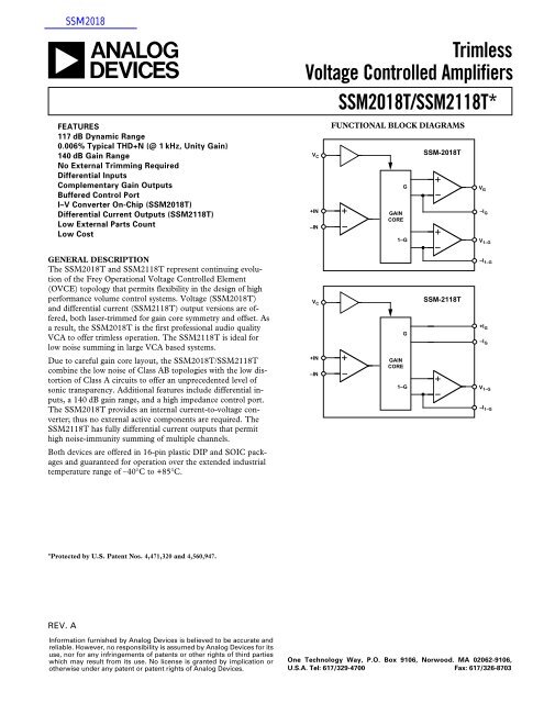
Trimless Voltage Controlled Amplifiers SSM2018T/SSM2118T*
Trimless Voltage Controlled Amplifiers SSM2018T/SSM2118T*
Trimless Voltage Controlled Amplifiers SSM2018T/SSM2118T*

You also want an ePaper? Increase the reach of your titles
YUMPU automatically turns print PDFs into web optimized ePapers that Google loves.
SSM1018T/SSM2118T–SPECIFICATIONS<br />
ELECTRICAL SPECIFICATIONS<br />
[VS = ±15 V, AV = 0 dB, RL = 100 kΩ, f = 1 kHz, 0 dBu = 0.775 V rms, simple VCA application<br />
circuit with 18 kΩ resistors, –VIN floating, and Class AB gain core bias (RB = 150 kΩ), –40°C < TA < +85°C, unless otherwise noted. Typical<br />
specifications apply at TA = +25°C.]<br />
Parameter Conditions Min Typ Max Units<br />
AUDIO PERFORMANCE 1<br />
Noise V IN = GND, 20 kHz Bandwidth –95 –93 dBu<br />
Headroom Clip Point = 1% THD+N +22 dBu<br />
Total Harmonic Distortion plus Noise 2nd and 3rd Harmonics Only (+25°C to +85°C)<br />
A V = 0 dB, V IN = +10 dBu 0.006 0.025 %<br />
AV = +20 dB, VIN = –10 dBu 0.013 0.04 %<br />
AV = –20 dB, VIN = +10 dBu 2<br />
0.013 0.04 %<br />
INPUT AMPLIFIER<br />
Bias Current V CM = 0 V 0.25 1 μA<br />
Offset <strong>Voltage</strong> V CM = 0 V 1 15 mV<br />
Offset Current VCM = 0 V 10 100 nA<br />
Input Impedance 4 MΩ<br />
Common-Mode Range ±13 V<br />
Gain Bandwidth VCA Configuration 0.7 MHz<br />
VCP Configuration 14 MHz<br />
Slew Rate 5 V/μs<br />
OUTPUT AMPLIFIER (<strong>SSM2018T</strong>)<br />
Offset <strong>Voltage</strong> V IN = 0 V, V C = +4 V 1.0 15 mV<br />
Output <strong>Voltage</strong> Swing I OUT = 1.5 mA<br />
Positive +10 +13 V<br />
Negative –10 –14 V<br />
Minimum Load Resistance For Full Output Swing 9 kΩ<br />
CONTROL PORT<br />
Bias Current 0.36 1 μA<br />
Input Impedance 1 MΩ<br />
Gain Constant Device Powered in Socket > 60 sec –30 mV/dB<br />
Gain Constant Temperature Coefficient –3500 ppm/°C<br />
Control Feedthrough 0 dB to –40 dB Gain Range ±1 ±4 mV<br />
Maximum Attenuation V C = +4 V 100 dB<br />
POWER SUPPLIES<br />
Supply <strong>Voltage</strong> Range ±5 ±18 V<br />
Supply Current 11 15 mA<br />
Power Supply Rejection Ratio 80 dB<br />
NOTES<br />
1SSM2118T tested and characterized using OP275 as current-to-voltage converter, see figure next page.<br />
2Guaranteed by characterization data and testing at AV = 0 dB.<br />
Specifications subject to change without notice.<br />
–2–<br />
REV. A
ABSOLUTE MAXIMUM RATINGS 1<br />
Supply <strong>Voltage</strong><br />
Dual Supply . . . . . . . . . . . . . . . . . . . . . . . . . . . . . . . . .±18 V<br />
Input <strong>Voltage</strong> . . . . . . . . . . . . . . . . . . . . . . . . . . . . . . . . . . . ±V S<br />
Operating Temperature Range . . . . . . . . . . . . .–40°C to +85°C<br />
Storage Temperature . . . . . . . . . . . . . . . . . . . –65°C to +150°C<br />
Junction Temperature (TJ) . . . . . . . . . . . . . . . . . . . . . +150°C<br />
Lead Temperature (Soldering, 60 sec) . . . . . . . . . . . . . +300°C<br />
THERMAL CHARACTERISTICS<br />
Thermal Resistance 2<br />
16-Pin Plastic DIP<br />
θ JA . . . . . . . . . . . . . . . . . . . . . . . . . . . . . . . . . . . . . . 76°C/W<br />
θ JC . . . . . . . . . . . . . . . . . . . . . . . . . . . . . . . . . . . . . . 33°C/W<br />
16-Pin SOIC<br />
θ JA . . . . . . . . . . . . . . . . . . . . . . . . . . . . . . . . . . . . . . 92°C/W<br />
θJC . . . . . . . . . . . . . . . . . . . . . . . . . . . . . . . . . . . . . . 27°C/W<br />
TRANSISTOR COUNT<br />
Number of Transistors<br />
<strong>SSM2018T</strong> . . . . . . . . . . . . . . . . . . . . . . . . . . . . . . . . . . 125<br />
SSM2118T . . . . . . . . . . . . . . . . . . . . . . . . . . . . . . . . . . 108<br />
ESD RATINGS<br />
883 (Human Body) Model . . . . . . . . . . . . . . . . . . . . . . . 500 V<br />
EIAJ Model . . . . . . . . . . . . . . . . . . . . . . . . . . . . . . . . . . . 100 V<br />
1 Stresses above those listed under “Absolute Maximum Ratings” may cause<br />
permanent damage to the device. This is a stress rating only and functional<br />
operation of the device at these or any other conditions above those indicated in the<br />
operation section of this specification is not implied. Exposure to absolute maximum<br />
rating conditions for extended periods may affect device reliability.<br />
2 θJA is specified for worst-case conditions, i.e., θJA is specified for device in socket<br />
for P-DIP and device soldered in circuit board for SOIC package.<br />
V IN+<br />
V IN–<br />
V+<br />
1μF<br />
18k<br />
1μF 18k<br />
1<br />
2<br />
50pF<br />
18k<br />
16<br />
15<br />
3<br />
14<br />
4 <strong>SSM2018T</strong><br />
13<br />
5<br />
6<br />
7<br />
12<br />
11<br />
10<br />
8 9<br />
47pF<br />
REV. A –3–<br />
150k<br />
1μF<br />
V OUT<br />
V–<br />
16-Lead Plastic DIP<br />
and SOL<br />
+I1–G 1<br />
16 V1–G<br />
V+ 2<br />
15 BAL<br />
–IG 3<br />
14 VG<br />
–I1–G 4 <strong>SSM2018T</strong> 13 GND<br />
COMP 1 5<br />
TOP VIEW<br />
(Not to Scale)<br />
12 MODE<br />
+IN 6<br />
11 VC<br />
–IN 7<br />
10 V–<br />
COMP 2 8 9 COMP 3<br />
<strong>SSM2018T</strong>/SSM2118T<br />
ORDERING GUIDE<br />
Model Temperature Range Package Option*<br />
<strong>SSM2018T</strong>P –40°C to +85°C N-16<br />
<strong>SSM2018T</strong>S –40°C to +85°C R-16<br />
SSM2118TP –40°C to +85°C N-16<br />
SSM2118TS –40°C to +85°C R-16<br />
*N = Plastic DIP; R = SOL.<br />
1μF 18k<br />
PIN CONFIGURATIONS<br />
16-Lead Plastic DIP<br />
and SOL<br />
BAL 1<br />
16 V+<br />
V1–G 2<br />
15 –IG<br />
+I1–G 3<br />
14 +IG<br />
–I1–G 4 SSM2118T 13 GND<br />
COMP 1 5<br />
TOP VIEW<br />
(Not to Scale)<br />
12 MODE<br />
+IN 6<br />
11 VC<br />
–IN 7<br />
10 V–<br />
COMP 2 8 9 COMP 3<br />
<strong>SSM2018T</strong> Typical Application Circuit SSM2118T Typical Application Circuit<br />
V IN+<br />
V IN–<br />
1μF 18k<br />
V–<br />
OPTIONAL<br />
TRIM<br />
1<br />
2<br />
5<br />
6<br />
7<br />
8<br />
47pF<br />
47k<br />
47k<br />
16<br />
15<br />
3<br />
14<br />
4<br />
SSM2118T<br />
13<br />
CAUTION<br />
ESD (electrostatic discharge) sensitive device. Electrostatic charges as high as 4000 V readily<br />
accumulate on the human body and test equipment and can discharge without detection.<br />
Although the <strong>SSM2018T</strong>/SSM2118T features proprietary ESD protection circuitry, permanent<br />
damage may occur on devices subjected to high energy electrostatic discharges. Therefore, proper<br />
ESD precautions are recommended to avoid performance degradation or loss of functionality.<br />
V+<br />
3k<br />
1k<br />
V CONTROL<br />
12<br />
11<br />
10<br />
9<br />
FROM<br />
ADDITIONAL<br />
SSM2118Ts<br />
V–<br />
V+<br />
150k<br />
470k<br />
50pF*<br />
10k<br />
10k<br />
1μF<br />
GLOBAL<br />
SYMMETRY<br />
TRIM<br />
500k 50pF<br />
18k<br />
18k<br />
A1<br />
A1, A2: OP275<br />
1k<br />
3k<br />
A2<br />
V OUT<br />
V CONTROL<br />
*FOR MORE THAN 2 SSM2118Ts<br />
WARNING!<br />
ESD SENSITIVE DEVICE
<strong>SSM2018T</strong>/SSM2118T–Typical Characteristics<br />
THD + N – %<br />
0.1<br />
0.010<br />
T A = +25°C<br />
V S = ±15V<br />
R F = 18kΩ<br />
AV = –20dB<br />
AV = 0dB<br />
AV = +20dB<br />
0.001<br />
20 100 1k<br />
FREQUENCY – Hz<br />
10k 20k<br />
Figure 1. <strong>SSM2018T</strong> THD + N Frequency (80 kHz Low-Pass<br />
Filter, for A V = 0 dB, V IN = 3 V rms; for A V = +20 dB,<br />
V IN = 0.3 V rms; for A V = –20 dB, V IN = 3 V rms)<br />
UNITS<br />
THD + N – %<br />
100<br />
90<br />
80<br />
70<br />
60<br />
50<br />
40<br />
30<br />
20<br />
10<br />
0<br />
0.000<br />
T A = +25°C<br />
A V = 0dB<br />
300 UNITS<br />
V IN = 10dBu<br />
V S = ±15V<br />
0.005<br />
0.010<br />
0.015<br />
DISTORTION – %<br />
0.020<br />
0.025<br />
Figure 2. <strong>SSM2018T</strong> Distortion Distribution<br />
1<br />
0.1<br />
0.010<br />
T A = +25°C<br />
R F = 18kΩ<br />
V S = ±15V<br />
0.001<br />
0.1 1<br />
AMPLITUDE – VRMS 10 20<br />
Figure 3. <strong>SSM2018T</strong> THD + N vs. Amplitude (Gain = 0 dB,<br />
fIN = 1 kHz, 80 kHz Low-Pass Filter)<br />
–4–<br />
THD + N – %<br />
1<br />
0.1<br />
0.010<br />
T A = +25°C<br />
V S = ±15V<br />
R F = 18kΩ<br />
0.001<br />
10m 0.1<br />
AMPLITUDE – VRMS 1 2<br />
Figure 4. <strong>SSM2018T</strong> THD + N vs. Amplitude<br />
(Gain = +20 dB, f IN =1 kHz, 80 kHz Low-Pass Filter)<br />
THD + N – %<br />
1.0<br />
0.1<br />
0.01<br />
T A = +25°C<br />
V S = ±15V<br />
R F = 18kΩ<br />
0.001<br />
–60 –40 –20<br />
0 20 40<br />
GAIN – dB<br />
Figure 5. <strong>SSM2018T</strong> THD + N vs. Gain (f IN = 1 kHz;<br />
for –60 dB ≤ A V ≤ –20 dB, V IN = 10 V rms;<br />
for 0 dB ≤ A V ≤ +20 dB, V IN = 1 V rms)<br />
THD + N – %<br />
0.1<br />
0.01<br />
T A = +25°C<br />
R F = 18kΩ<br />
0.001<br />
0 ±3 ±6 ±9 ±12 ±15 ±18<br />
SUPPLY VOLTAGE – Volts<br />
Figure 6. <strong>SSM2018T</strong> THD + N vs. Supply <strong>Voltage</strong><br />
(AV = 0 dB, VIN = 1 V rms, fIN = 1 kHz, 80 kHz<br />
Low-Pass Filter)<br />
REV. A
NOISE DENSITY – nV/√Hz<br />
Figure 7. <strong>SSM2018T</strong> Noise Density vs. Frequency<br />
OUTPUT VOLTAGE SWING – V PEAK<br />
±20<br />
±15<br />
±10<br />
±5<br />
0<br />
0<br />
R F = 18kΩ<br />
T A = +25°C<br />
±5<br />
±10<br />
REV. A –5–<br />
±15<br />
R L = ∞Ω<br />
SUPPLY VOLTAGE – Volts<br />
R L = 10kΩ<br />
Figure 8. <strong>SSM2018T</strong> Maximum Output Swing vs.<br />
Supply <strong>Voltage</strong> (THD = 1% max)<br />
MAXIMUM OUTPUT SWING – V PEAK<br />
500<br />
400<br />
300<br />
200<br />
100<br />
±15<br />
±12<br />
0<br />
10<br />
±9<br />
±6<br />
±3<br />
T A = +25°C<br />
V S = ±15V<br />
R F = 18kΩ<br />
T A = +25°C<br />
V S = ±15V<br />
100 1k<br />
10k<br />
100k<br />
FREQUENCY – Hz<br />
R L = ∞<br />
R L = 10k<br />
±20<br />
0<br />
1k 10k<br />
FREQUENCY – Hz<br />
100k<br />
Figure 9. <strong>SSM2018T</strong> Maximum Output Swing vs.<br />
Frequency (THD = 1 % max)<br />
MAXIMUM OUTPUT SWING – V PEAK<br />
±15<br />
±12<br />
±9<br />
±6<br />
±3<br />
R F = 18kΩ<br />
T A = +25°C<br />
V S = ±15V<br />
<strong>SSM2018T</strong>/SSM2118T<br />
0<br />
100 1k 10k<br />
100k<br />
LOAD RESISTANCE – Ω<br />
Figure 10. <strong>SSM2018T</strong> Maximum Output Swing vs.<br />
Load Resistance, (THD = 1 % max)<br />
GAIN – dB<br />
OUTPUT OFFSET – mV<br />
100<br />
90<br />
80<br />
70<br />
60<br />
50<br />
40<br />
30<br />
20<br />
10<br />
0<br />
–80<br />
T A = +25°C<br />
V S = ±15V<br />
–60<br />
–40<br />
–20<br />
GAIN – dB<br />
Figure 11. <strong>SSM2018T</strong> Output Offset vs. Gain<br />
+10<br />
+5<br />
0<br />
–5<br />
–10<br />
–15<br />
100<br />
T A = +25°C<br />
V S = ±15V<br />
PHASE<br />
–135<br />
1k 10k<br />
100k<br />
1M<br />
FREQUENCY – Hz<br />
0<br />
20<br />
GAIN<br />
Figure 12. <strong>SSM2018T</strong> Gain/Phase vs. Frequency<br />
0<br />
40<br />
–45<br />
–90<br />
PHASE – Degrees
<strong>SSM2018T</strong>/SSM2118T–Typical Characteristics<br />
GAIN – dB<br />
THD + N – %<br />
60<br />
40<br />
20<br />
0<br />
–20<br />
–40<br />
–60<br />
T A = +25°C<br />
V S = ±15V<br />
–80<br />
100 1k 10k 100k 1M 10M<br />
FREQUENCY – Hz<br />
Figure 13. <strong>SSM2018T</strong> Gain vs. Frequency<br />
0.1<br />
0.010<br />
T A = +25°C<br />
R F = 18kΩ<br />
A V = 0dB<br />
A V = +20dB<br />
A V = –20dB<br />
0.001<br />
20 100 1k<br />
FREQUENCY – Hz<br />
10k 20k<br />
Figure 14. SSM2118T THD + N Frequency (80 kHz<br />
Low-Pass Filter, for A V = 0 dB, V IN = 1 V rms;<br />
for A V = +20 dB, V IN = 0.1 V rms; for A V = –20 dB,<br />
V IN = 10 V rms)<br />
UNITS<br />
100<br />
90<br />
80<br />
70<br />
60<br />
50<br />
40<br />
30<br />
20<br />
10<br />
0<br />
0.000<br />
0.005<br />
0.010<br />
0.015<br />
DISTORTION – %<br />
T A = +25°C<br />
A V = 0dB<br />
300 UNITS<br />
V IN = 10dBu<br />
V S = ±15V<br />
0.020<br />
0.025<br />
Figure 15. SSM2118T Distortion Distribution<br />
–6–<br />
THD + N – %<br />
1<br />
0.1<br />
0.010<br />
T A = +25°C<br />
V S = ±15V<br />
0.001<br />
0.1 1<br />
AMPLITUDE – VRMS 10 20<br />
Figure 16. SSM2118T THD + N vs. Amplitude<br />
(Gain = 0 dB, f IN = 1 kHz, 80 kHz Low-Pass Filter)<br />
THD + N – %<br />
1<br />
0.1<br />
0.010<br />
T A = +25°C<br />
V S = ±15V<br />
0.001<br />
10m 0.1<br />
AMPLITUDE – VRMS 1 2<br />
Figure 17. SSM2118T THD + N vs. Amplitude<br />
(Gain = +20 dB, f IN = 1 kHz, 80 kHz Low-Pass Filter)<br />
THD + N – %<br />
1.0<br />
0.1<br />
0.01<br />
0.001<br />
–60 –40 –20 0 +20 +40<br />
GAIN – dB<br />
T A = +25°C<br />
V S = ±15V<br />
Figure 18. SSM2118T THD + N vs. Gain (fIN = 1 kHz;<br />
for –60 dB ≤ A V ≤ –20 dB, V IN = 10 V rms;<br />
for 0 dB ≤ A V ≤ +20 dB, V IN = 1 V rms)<br />
REV. A
THD + N – %<br />
0.1<br />
0.01<br />
T A = +25°C<br />
0.001<br />
0 ±3 ±6 ±9 ±12 ±15 ±18<br />
SUPPLY VOLTAGE – Volts<br />
Figure 19. SSM2118T THD + N vs. Supply <strong>Voltage</strong><br />
(AV = 0 dB, VIN = 1 V rms, fIN = 1 kHz, 80 kHz<br />
Low-Pass Filter)<br />
NOISE DENSITY – nV/√Hz<br />
Figure 20. SSM2118T Noise Density vs. Frequency<br />
OUTPUT VOLTAGE SWING – V PEAK<br />
500<br />
400<br />
300<br />
200<br />
100<br />
±20<br />
±20<br />
±15<br />
±10<br />
±5<br />
T A = +25°C<br />
V S = ±15V<br />
0<br />
10 100 1k 10k 100k<br />
T A = +25°C<br />
FREQUENCY – Hz<br />
0<br />
0 ±5 ±10 ±15 ±20<br />
SUPPLY VOLTAGE – Volts<br />
R L = ∞Ω<br />
Figure 21. SSM2118T Maximum Output Swing vs.<br />
Supply <strong>Voltage</strong> (THD = 1% max)<br />
REV. A –7–<br />
MAXIMUM OUTPUT SWING – V PEAK<br />
±15<br />
±12<br />
±9<br />
±6<br />
±3<br />
T A = +25°C<br />
V S = ±15V<br />
<strong>SSM2018T</strong>/SSM2118T<br />
0<br />
1k 10k<br />
FREQUENCY – Hz<br />
100k<br />
Figure 22. SSM2118T Maximum Output Swing vs.<br />
Frequency (THD = 1 % max)<br />
OUTPUT OFFSET CURRENT – µA<br />
10<br />
9<br />
8<br />
7<br />
6<br />
5<br />
4<br />
3<br />
2<br />
1<br />
0<br />
–80<br />
T A = +25°C<br />
V S = ±15V<br />
–60<br />
–40<br />
–20<br />
GAIN – dB<br />
Figure 23. SSM2118T Output Offset Current vs. Gain<br />
GAIN – dB<br />
+10<br />
+5<br />
0<br />
–5<br />
–10<br />
–15<br />
100<br />
T A = +25°C<br />
V S = ±15V<br />
PHASE<br />
1k 10k<br />
100k<br />
1M<br />
FREQUENCY – Hz<br />
0<br />
20<br />
GAIN<br />
0<br />
40<br />
–45<br />
–90<br />
PHASE – Degrees<br />
–135<br />
Figure 24. SSM2118T Gain/Phase vs. Frequency
<strong>SSM2018T</strong>/SSM2118T<br />
GAIN – dB<br />
DISTORTION – %<br />
60<br />
40<br />
20<br />
0<br />
–20<br />
–40<br />
–60<br />
–80<br />
100 1k 10k 100k 1M 10M<br />
FREQUENCY – Hz<br />
T A = +25°C<br />
V S = ±1.5V<br />
OP275 AS<br />
I/V CONV.<br />
Figure 25. SSM2118T Gain vs. Frequency<br />
0.06<br />
0.05<br />
0.04<br />
0.03<br />
0.02<br />
0.01<br />
0<br />
–40<br />
V IN = 10dBu<br />
A V = 0dB<br />
–20<br />
V IN = 10dBu<br />
A V = –20dB<br />
AND<br />
V IN = –10dBu<br />
A V = 20dB<br />
0 20 40 60<br />
TEMPERATURE – °C<br />
T A = +25°C<br />
V S = ±15V<br />
Figure 26. <strong>SSM2018T</strong> and SSM2118T Distortion vs.<br />
Temperature<br />
OUTPUT NOISE – dBu<br />
–60<br />
–70<br />
–80<br />
–90<br />
–100<br />
–110<br />
–60<br />
–40<br />
T A = +25°C<br />
V S = ±15V<br />
–20<br />
GAIN – dB<br />
Figure 27. <strong>SSM2018T</strong> and SSM2118T Output Noise vs.<br />
Gain (VIN = GND, 20 kHz Bandwidth)<br />
0<br />
20<br />
80<br />
100<br />
40<br />
–8–<br />
UNITS<br />
100<br />
90<br />
80<br />
70<br />
60<br />
50<br />
40<br />
30<br />
20<br />
10<br />
TA = +25°C<br />
0V < VC < 1.2V<br />
FREQ = 0Hz<br />
300 UNITS<br />
0<br />
–3.0 –2.0 –1.0 0 1.0 2.0<br />
CONTROL FEEDTHROUGH – mV<br />
Figure 28. <strong>SSM2018T</strong> Control Feedthrough Distribution<br />
CONTROL FEEDTHROUGH – dB<br />
0<br />
–20<br />
–40<br />
–60<br />
–80<br />
V S = ±15V<br />
T A = +25°C<br />
V C = 100mV RMS<br />
–100<br />
100 1k 10k<br />
100k<br />
FREQUENCY – Hz<br />
Figure 29. <strong>SSM2018T</strong> and SSM2118T Control<br />
Feedthrough vs. Frequency<br />
CONTROL FEEDTHROUGH – mV<br />
3<br />
2<br />
1<br />
0<br />
–1<br />
–2<br />
–3<br />
–40<br />
–20<br />
V S = ±15V<br />
0V < V C < 1.2V<br />
FREQ = 0Hz<br />
0 20 40 60<br />
TEMPERATURE – °C<br />
Figure 30. <strong>SSM2018T</strong> and SSM2118T Control<br />
Feedthrough vs. Temperature<br />
80<br />
100<br />
REV. A
GAIN CONSTANT – mV/dB<br />
–20<br />
–25<br />
–30<br />
–35<br />
V S = ±15V<br />
–40<br />
–40 –20 0 20 40 60 80 100<br />
TEMPERATURE – °C<br />
Figure 31. <strong>SSM2018T</strong> and SSM2118T Gain Constant vs.<br />
Temperature<br />
GAIN CONSTANT – mV/dB<br />
–28<br />
–29<br />
–30<br />
–31<br />
–32<br />
–33<br />
–80<br />
T A = +25°C<br />
V S = ±15V<br />
–60<br />
–40<br />
–20<br />
REV. A –9–<br />
0<br />
GAIN – dB<br />
Figure 32. <strong>SSM2018T</strong> and SSM2118T Gain Constant<br />
Linearity vs. Gain<br />
GAIN – dB<br />
0.1<br />
0.0<br />
–0.1<br />
–0.2<br />
–0.3<br />
–0.4<br />
100 1k 10k<br />
FREQUENCY – Hz<br />
100k<br />
20<br />
40<br />
T A = +25°C<br />
V S = ±15V<br />
A V = 0dB<br />
V IN = 100V RMS<br />
Figure 33. <strong>SSM2018T</strong> and SSM2118T Gain Flatness vs.<br />
Frequency<br />
60<br />
CMRR – dB<br />
0<br />
–20<br />
–40<br />
–60<br />
–80<br />
–100<br />
10<br />
V S = ±15V<br />
T A = +25°C<br />
<strong>SSM2018T</strong>/SSM2118T<br />
100 1k<br />
FREQUENCY – Hz<br />
10k<br />
100k<br />
Figure 34. <strong>SSM2018T</strong> and SSM2118T CMRR vs.<br />
Frequency<br />
SLEW RATE – V/µs<br />
15.0<br />
12.5<br />
10.0<br />
7.5<br />
5.0<br />
2.5<br />
0<br />
0<br />
T A = +25°C<br />
±5<br />
±10<br />
SUPPLY VOLTAGE – Volts<br />
+ SLEW RATE<br />
– SLEW RATE<br />
Figure 35. <strong>SSM2018T</strong> and SSM2118T Slew Rate vs.<br />
Supply <strong>Voltage</strong><br />
PSRR – dB<br />
0<br />
–20<br />
–40<br />
–60<br />
–80<br />
–100<br />
10<br />
VS = ±15V<br />
TA = +25°C<br />
+ PSRR<br />
– PSRR<br />
±15<br />
100 1k<br />
FREQUENCY – Hz<br />
10k<br />
100k<br />
Figure 36. <strong>SSM2018T</strong> and SSM2118T PSRR vs. Frequency
<strong>SSM2018T</strong>/SSM2118T<br />
APPLICATIONS<br />
The <strong>SSM2018T</strong> is a trimless <strong>Voltage</strong> <strong>Controlled</strong> Amplifier<br />
(VCA) for volume control in audio systems. The <strong>SSM2018T</strong> is<br />
identical to the original SSM2018 in functionality and pinout;<br />
however, it is the first professional quality audio VCA<br />
in the marketplace that does not require an external trimming<br />
potentiometer to minimize distortion. Instead, the<br />
<strong>SSM2018T</strong> is laser trimmed before it is packaged to ensure the<br />
specified THD and control feedthrough performance. This has<br />
a significant savings in not only the cost of external trimming<br />
potentiometers, but also the manufacturing cost of performing<br />
the trimming during production.<br />
The SSM2118T is identical to the <strong>SSM2018T</strong> except that differential<br />
current outputs are provided as opposed to a voltage<br />
output. This output configuration is ideal for bus summing applications<br />
where multiple audio signals are summed together.<br />
These signals often require long lead lengths or cable runs to<br />
reach the summing stage. Transmitting the signals in a differential<br />
current mode minimizes the chance for noise pickup and for<br />
line impedances to upset the balance of the system. The<br />
SSM2118T is also factory trimmed to minimize distortion and<br />
control feedthrough. Thus, no individual trim is required for<br />
each part. One global trim at the summing amplifier stage may<br />
be necessary to properly balance the resistors in this stage, as explained<br />
later.<br />
Basic VCA Configuration<br />
The primary application circuit for the <strong>SSM2018T</strong> is the basic<br />
VCA configuration, which is shown in Figure 37. This configuration<br />
uses differential current feedback to realize the VCA. A<br />
complete description of the internal circuitry of the VCA and<br />
this configuration is given in the Theory of Operation section<br />
below. The <strong>SSM2018T</strong> and SSM2118T are trimmed at the factory<br />
for operation in the basic VCA configuration with class AB biasing.<br />
Thus, for optimal distortion and control feedthrough performance,<br />
the same configuration and biasing should be used. All<br />
of the graphs for the <strong>SSM2018T</strong> in the data sheet have been<br />
measured using the circuit of Figure 37.<br />
V IN+<br />
V IN–<br />
V+<br />
1μF<br />
18k<br />
1μF 18k<br />
1<br />
2<br />
50pF<br />
18k<br />
16<br />
15<br />
3<br />
14<br />
4 <strong>SSM2018T</strong> 13<br />
5<br />
6<br />
7<br />
12<br />
11<br />
10<br />
8 9<br />
47pF<br />
R B<br />
150k<br />
1μF<br />
V OUT<br />
V–<br />
V+<br />
3k<br />
1k<br />
V CONTROL<br />
Figure 37. <strong>SSM2018T</strong> Basic VCA Application Circuit<br />
In the simple VCA configuration, the <strong>SSM2018T</strong> inputs are at a<br />
virtual ground. Thus, 18 kΩ resistors are required to convert<br />
the input voltages to input currents. The schematic also shows<br />
ac coupling capacitors. These are inserted to minimize dc offsets<br />
generated by bias current through the resistors. Without the<br />
capacitors, the dc offset due to the input bias current is typically<br />
5 mV. The input stage has the flexibility to run either inverting,<br />
noninverting, or balanced. The most common configuration is<br />
–10–<br />
to run it in the noninverting single-ended mode. If either input<br />
is unused, the associated 18 kΩ resistor and coupling capacitor<br />
should be removed to prevent any additional noise.<br />
The common-mode rejection in balanced mode is typically<br />
55 dB up to 1 kHz, decreasing at higher frequencies as shown in<br />
Figure 34. To ensure good CMRR in the balanced configuration,<br />
the input resistors must be balanced. For example, a 1%<br />
mismatch results in a CMRR of 40 dB. To achieve 55 dB,<br />
these resistors should have an absolute tolerance match of 0.1%.<br />
The output of the basic VCA is taken from Pin 14, which is the<br />
output of an internal amplifier. Notice that the second voltage<br />
output (Pin 16) is connected to the negative supply. This is<br />
normal and actually disables that output amplifier ensuring that<br />
it will not oscillate and cause interference problems. Shorting<br />
the output to the negative supply does not cause the supply current<br />
to increase. This amplifier is only used in the “OVCE” application<br />
explained later.<br />
The control port follows a 30 mV/dB control law. The application<br />
circuit shows a 3 kΩ and 1 kΩ resistor divider from a control<br />
voltage. The choice of these resistors is arbitrary and could<br />
be any values to properly scale the control voltage. In fact, these<br />
resistors could be omitted if the control voltage is already properly<br />
scaled. The 1 μF capacitor is in place to provide some filtering<br />
of the control signal. Although the control feedthrough is<br />
trimmed at the factory, the feedthrough increases with frequency<br />
(Figure 29). Thus, high frequency noise can<br />
feedthrough and add to the noise of the VCA. Filtering the<br />
control signal helps minimize this source of noise.<br />
Theory of Operation of the <strong>SSM2018T</strong><br />
The <strong>SSM2018T</strong> has the same internal circuitry as the original<br />
SSM2018. The detailed diagram in Figure 38 shows the main<br />
components of the VCA. The essence of the <strong>SSM2018T</strong> is the<br />
gain core, which is comprised of two differential pairs (Q1–Q4).<br />
When the control voltage, VC, is adjusted, current through the<br />
gain core is steered to one side or the other of the two differential<br />
pairs. The tail current for these differential pairs is set by<br />
the mode bias of the VCA (Class A or AB), which is labeled as<br />
IM in the diagram. IM is then modulated by a current proportional<br />
to the input voltage, labeled IS. For a positive input voltage,<br />
more current is steered (by the “Splitter”) to the left<br />
differential pair, and the opposite is true for a negative input.<br />
To understand how the gain control works, a simple example is<br />
best. Take the case of a positive control voltage on Pin 11. Notice<br />
that the bases of Q2 and Q3 are connected to ground via a<br />
200 Ω resistor. A positive control voltage produces a positive<br />
voltage on the bases of Q1 and Q4. Concentrating on the left<br />
most differential pair, this raises the base voltage of Q1 above<br />
that of Q2. Thus, more of the tail current is steered through Q1<br />
than through Q2. The current from the collector of Q2 flows<br />
through the external 18 kΩ feedback resistor around amplifier<br />
A3. When this current is reduced, the output voltage is also reduced.<br />
Thus, a positive control voltage results in an attenuation<br />
of the input signal, which explains why the gain constant is<br />
negative.<br />
The collector currents of Q2 and Q3 produce the output voltage.<br />
The output of Q3 is mirrored by amplifier A1 to add to the<br />
overall output voltage. On the other hand, the collector currents<br />
of Q1 and Q4 are used for feedback to the differential inputs.<br />
Because Pins 6 and 4 are shorted together, any input<br />
voltage produces an input current which flows into Pin 4. The<br />
REV. A
same is true for the inverting input, which is connected to Pin 1.<br />
The overall feedback ensures that the current flowing through<br />
the input resistors is balanced by the collector currents in Q1<br />
and Q4.<br />
Basic VCA Configuration for the SSM2118T<br />
The SSM2118T behaves very much in the same way as the<br />
<strong>SSM2018T</strong> except that it has differential current outputs instead<br />
of a voltage output. The basic VCA configuration is<br />
shown in Figure 39. A dual output amplifier is needed to replace<br />
the internal amplifiers in the <strong>SSM2018T</strong>. However, multiple<br />
SSM2118Ts can share the output amplifiers. The op amps<br />
are configured so that the SSM2118T’s output current is flowing<br />
into a virtual ground. This same virtual ground is presented<br />
to all the VCAs, allowing their currents to be summed without<br />
interaction.<br />
V IN+<br />
V IN–<br />
1μF 18k<br />
1μF 18k<br />
V–<br />
–IN<br />
+IN<br />
V–<br />
7<br />
6<br />
10<br />
OPTIONAL<br />
TRIM<br />
1<br />
2<br />
5<br />
6<br />
7<br />
8<br />
47pF<br />
V+<br />
2<br />
47k<br />
47k<br />
16<br />
15<br />
3<br />
14<br />
4<br />
SSM2118T<br />
13<br />
12<br />
11<br />
10<br />
9<br />
FROM<br />
ADDITIONAL<br />
SSM2118Ts<br />
REV. A –11–<br />
V–<br />
COMP 2<br />
V+<br />
150k<br />
8 5<br />
470k<br />
50pF*<br />
10k<br />
10k<br />
1μF<br />
COMP 1<br />
COMPENSATION<br />
NETWORK<br />
GLOBAL<br />
SYMMETRY<br />
TRIM<br />
500k 50pF<br />
18k<br />
18k<br />
A1<br />
A1, A2: OP275<br />
1k<br />
3k<br />
A2<br />
V OUT<br />
V CONTROL<br />
*FOR MORE THAN 2 SSM2118Ts<br />
Figure 39. SSM2118T Typical Bus Summing Application<br />
9<br />
COMP 3<br />
VG<br />
14<br />
A3<br />
–I G<br />
3 1<br />
1–G G G 1–G<br />
GAIN<br />
CORE<br />
Q1 Q2 Q3 Q4<br />
Im+( Is )<br />
2<br />
200<br />
A1<br />
SPLITTER<br />
+I 1-G<br />
Im–( Is )<br />
2<br />
200<br />
VREF<br />
Figure 38. <strong>SSM2018T</strong> Detailed Functional Diagram<br />
A2<br />
Im<br />
<strong>SSM2018T</strong>/SSM2118T<br />
1.8k<br />
A global symmetry trim may be necessary, but since it is at the<br />
output amplifiers, only one trim is needed for any number of<br />
SSM2118Ts connected to the summing bus. This trim balances<br />
the resistors around the two amplifiers. If precision,<br />
matched resistors are used, the trim can be removed. However,<br />
to achieve 0.006% distortion, these resistors need to be matched<br />
to approximately 0.01%.<br />
If the choice is made to perform the trim, then one of two methods<br />
may be used. The first method minimizes the distortion of<br />
an audio signal with the SSM2118T in the circuit. To perform<br />
the trim, a 0 dBu, 1 kHz sine wave is applied to one of the<br />
VCAs, and the output distortion is monitored. As the symmetry<br />
trim is adjusted, the output distortion will vary. The optimal<br />
adjustment produces the lowest distortion over the entire trim<br />
range. The second method is to insert a common mode signal<br />
by connecting two 47 kΩ resistors (matched to 0.01%) to the<br />
inverting inputs of each amplifier, as shown in the Figure 39.<br />
The signal is typically a 0 dBu, 1 kHz sine wave, although other<br />
signals can be used. The output is monitored with an oscilloscope,<br />
and the potentiometer is adjusted to achieve a minimum<br />
output signal.<br />
The SSM2118T has the exact same input and gain core construction<br />
as the <strong>SSM2018T</strong>. Thus, any discussion of these portions<br />
of the <strong>SSM2018T</strong> apply equally to the SSM2118T. The<br />
main difference, which is apparent by comparing Figure 40 to<br />
Figure 38, is the removal of two output amplifiers, A1 and A3.<br />
Instead, the output currents come directly from the collectors of<br />
Q2 and Q3. Notice that the two external amplifiers in Figure<br />
39 are configured the same as the internal amplifiers in the<br />
<strong>SSM2018T</strong>.<br />
Two important characteristics of these current outputs must be<br />
considered: the output compliance and the effects of capacitive<br />
loading. Normally, the outputs are connected to a virtual<br />
ground node at the summing stage, which is biased at ground.<br />
This bias point can be altered somewhat. The part maintains<br />
good distortion performance for an output compliance from<br />
A4<br />
15<br />
4<br />
16<br />
11<br />
13<br />
12<br />
BAL<br />
–I 1-G<br />
V 1-G<br />
V C<br />
GND<br />
MODE
<strong>SSM2018T</strong>/SSM2118T<br />
V+<br />
–IN<br />
+IN<br />
V–<br />
16<br />
7<br />
6<br />
10<br />
COMP 2 COMP 1<br />
8 5<br />
COMPENSATION<br />
NETWORK<br />
9<br />
COMP 3<br />
–0.1 V to +6.0 V. The negative compliance is much smaller because<br />
the gain core transistors (Q1 and Q3) begin to saturate<br />
when the collector potential is brought below their base potential.<br />
These outputs have high immunity to capacitive loads. In<br />
fact, the load on either or both outputs can be as large as 10 nF<br />
with no change in the distortion performance. For values above<br />
10 nF, the distortion does start to increase. For example, a<br />
100 nF load causes the distortion to increase from 0.006% to<br />
0.02% at 1 kHz.<br />
The noise performance of a single SSM2118T with an OP275<br />
output amplifier is shown in Figure 20. When multiple<br />
SSM2118T parts are operated in parallel, the noise does increase<br />
by a factor equal to the square root of the number of<br />
parts paralleled. For example, if five parts are in parallel, the<br />
total output noise is 100 nV√(Hz) × √5 = 220 nV/√Hz.<br />
–IG<br />
15<br />
–12–<br />
200<br />
14<br />
A2<br />
1–G G G 1–G<br />
GAIN<br />
CORE<br />
Q1 Q2 Q3 Q4<br />
Im+( Is )<br />
2<br />
Compensating the <strong>SSM2018T</strong> and SSM2118T<br />
Both parts employ the same compensation network. This network<br />
uses an adaptive compensation scheme that adjusts the optimum<br />
compensation level for a given gain. The control voltage<br />
not only adjusts the gain core steering, it also adjusts the compensation.<br />
The <strong>SSM2018T</strong> and SSM2118T have three compensation<br />
pins: COMP1, COMP2, and COMP3. COMP3 is<br />
normally left open. Grounding this pin actually defeats the<br />
adaptive compensation circuitry, giving the VCA a fixed compensation<br />
point. The only time that this is desirable is when the<br />
VCA has fixed feedback, such as the <strong>Voltage</strong> <strong>Controlled</strong> Panner<br />
(VCP) circuit shown later in the data sheet. Thus, for the Basic<br />
VCA circuit or the OVCE circuit, COMP3 should be left open.<br />
A compensation capacitor does need to be added between<br />
COMP1 and COMP2. Because the VCA operates over such a<br />
wide gain range, ideally the compensation should be optimized<br />
for each gain. When the VCA is in high attenuation, there is<br />
very little “loop gain,” and the part needs to have high compensation.<br />
On the other hand, at high gain, the same compensation<br />
capacitor would overcompensate the part and roll off the high<br />
frequency performance. Thus, the <strong>SSM2018T</strong> and SSM2118T<br />
SPLITTER<br />
+IG<br />
+I1–G<br />
3<br />
Im–( Is )<br />
2<br />
200<br />
VREF<br />
Figure 40. SSM2118T Detailed Functional Diagram<br />
Im<br />
1.8k<br />
A4<br />
1<br />
4<br />
2<br />
11<br />
13<br />
12<br />
BAL<br />
–I1–G<br />
V1–G<br />
VC<br />
GND<br />
MODE<br />
employ a patented adaptive compensation circuit. The compensation<br />
capacitor is “Miller” connected between the base and collector<br />
of an internal transistor. By changing the gain of this<br />
transistor via the control voltage, the compensation is changed.<br />
Increasing the compensation capacitor causes the frequency response<br />
and slew rate to decrease, which will tend to cause high<br />
frequency distortion to increase. For the basic VCA circuit,<br />
47 pF was chosen as the optimal value. The OVCE circuit described<br />
later uses a 220 pF capacitor. The reason for the increase<br />
is to compensate for the extra phase shift from the<br />
additional output amplifier used in the OVCE configuration.<br />
The compensation capacitor can be adjusted over a practical<br />
range from 47 pF to 220 pF, if desired. Below 47 pF, the parts<br />
may oscillate, and above 220 pF the frequency response is significantly<br />
degraded.<br />
Control Section<br />
As mentioned before, the control voltage on Pin 11 steers the<br />
current through the gain core transistors to set the gain. The<br />
output gain formula is as follows:<br />
V OUT = V IN × e(–aV C )<br />
The exponential term arises from the standard Ebers-Moll<br />
equation describing the relationship of a transistor’s collector<br />
current as a function of the base-emitter voltage:<br />
I C = I S × e (V BE /V T ) .<br />
The factor “a” is a function of not only V T but also the scaling<br />
due to the resistor divider of the 200 Ω and 1.8 kΩ resistors<br />
shown in Figures 38 and 40. The resulting expression for “a” is<br />
as follows: a = 1/(10 × VT) which is approximately equal to four<br />
at room temperature. Substituting a = 4 in the above equation<br />
results in a –28.8 mV/dB control law at room temperature.<br />
The –28.8 mV/dB number is slightly different from the data<br />
sheet specification of –30 mV/dB. The difference arises from<br />
the temperature dependency of the control law. The term VT<br />
is known as the thermal voltage, and it has a direct dependency<br />
REV. A
on temperature: VT = kT/q (k = Boltzmann’s constant =<br />
1.38E-23, q = electron charge = 1.6E-19, and T = absolute<br />
temperature in Kelvin). This temperature dependency leads to<br />
the –3500 ppm/°C drift of the control law. It also means that<br />
the control law changes as the part warms up. Thus, our specification<br />
for the control law states that the part has been powered<br />
up for 60 seconds.<br />
When the part is initially turned on, the temperature of the die<br />
is still at the ambient temperature (25°C for example), but the<br />
power dissipation causes the die to warm up. With ±15 V supplies<br />
and a supply current of 11 mA, 330 mW is dissipated.<br />
This number is multiplied by θJA to determine the rise in the<br />
die’s temperature. In this case, the die increases from 25°C to<br />
approximately 50°C. A 25°C temperature change causes a<br />
8.25% increase in the gain constant, resulting in a gain constant<br />
of 30 mV/dB. The graph in Figure 31 shows how the gain constant<br />
varies over the full temperature range.<br />
Proper Operating Mode for the <strong>SSM2018T</strong> and SSM2118T<br />
Both parts have the flexibility of operating in either Class A or<br />
Class AB. This is accomplished by adjusting the amount of current<br />
flowing in the gain core (IM in Figure 38). The traditional<br />
trade-off between the two classes is that Class A tends to have<br />
lower THD but higher noise than Class AB. However, by utilizing<br />
well matched gain core transistors, distortion compensation<br />
circuitry, and laser trimming, the <strong>SSM2018T</strong> and SSM2118T<br />
have excellent THD performance in Class AB. Thus, the parts<br />
offer the best of both worlds in having the low noise of Class AB<br />
with low THD.<br />
Because the parts operate optimally in Class AB, the distortion<br />
trim is performed for this class. To guarantee conformance to the<br />
data sheet THD specifications, both the <strong>SSM2018T</strong> and SSM2118T<br />
must be operated in Class AB. This does not mean that the parts<br />
cannot be operated in Class A, but the optimal THD trim point<br />
is different for the two classes. Using Class A operation results<br />
in a shift of THD performance from a typical value of 0.006%<br />
to 0.05% without trim. An external potentiometer could be<br />
added to change the trim back to its optimal point as shown in<br />
the OVCE application circuit, but this adds the expense and<br />
time in adjusting a potentiometer.<br />
The class of operation is set by selecting the proper value for RB<br />
shown in Figure 37. RB determines the current flowing into the<br />
MODE input (Pin 12). For class AB operation with ±15 V<br />
supplies, RB should be 150 kΩ. This results in a current of 95<br />
μA. For other supply voltages, adjust the value of RB such that<br />
current remains at 95 μA. This current follows the formula:<br />
I MODE = (V CC –0.7V)<br />
RB The factor of 0.7 V arises from the fact that the dc bias on Pin<br />
12 is a diode drop above ground.<br />
Output Drive<br />
The <strong>SSM2018T</strong> is buffered by an internal op amp to provide a<br />
low impedance output. This output is capable of driving to<br />
within 1.2 V of either rail at 1% distortion for a 100 kΩ load.<br />
(Note: This 100 kΩ load is in parallel with the feedback resistor<br />
of 18 kΩ, so the effective load is 15.3 kΩ.) For better than<br />
0.01% distortion, the output should remain about 3.5 V away<br />
from either rail as shown in Figure 3. As the graph of output<br />
REV. A –13–<br />
<strong>SSM2018T</strong>/SSM2118T<br />
swing versus load resistance shows (Figure 10), to maintain less<br />
than 1% distortion, the output current should be limited to<br />
approximately ±1.3 mA. If higher current drive is required,<br />
then the output should be buffered with a high quality op amp<br />
such as the OP176 or AD797.<br />
The internal amplifiers are compensated for unity gain stability<br />
and are capable of driving a capacitive load up to 4700 pF.<br />
Larger capacitive loads should be isolated from the output of the<br />
<strong>SSM2018T</strong> by the use of a 50 Ω series resistor.<br />
Upgrading SSM2018 Sockets<br />
The <strong>SSM2018T</strong> easily replaces the SSM2018 in the basic VCA<br />
configuration. The parts are pin for pin compatible allowing direct<br />
replacement. At the same time, the trimming potentiometers<br />
for symmetry and offset should be removed, as shown in<br />
Figure 41. Upgrading to the <strong>SSM2018T</strong> immediately saves the<br />
expense of the potentiometers and the time in production of<br />
trimming for minimum distortion and control feedthrough.<br />
V IN+<br />
V IN–<br />
V+<br />
V–<br />
OFFSET<br />
TRIM 10MΩ<br />
100kΩ<br />
V+<br />
1µF 18kΩ<br />
1µF 18kΩ<br />
REMOVE FOR <strong>SSM2018T</strong><br />
SYMMETRY<br />
TRIM<br />
470kΩ<br />
500kΩ<br />
47pF<br />
RB: 150kΩ FOR CLASS AB<br />
NC = NO CONNECT<br />
1<br />
2<br />
3<br />
4<br />
5<br />
6<br />
7<br />
8<br />
50pF<br />
18kΩ<br />
16<br />
15<br />
14<br />
13<br />
<strong>SSM2018T</strong><br />
12<br />
11<br />
10<br />
9<br />
NC<br />
V–<br />
R B<br />
1µF<br />
V OUT<br />
V+<br />
3kΩ<br />
1kΩ<br />
V CONTROL<br />
Figure 41. Upgrading SSM2018 Sockets<br />
If the SSM2018 is used in the OVCE or VCP configuration, the<br />
<strong>SSM2018T</strong> can still directly replace it. However, the potentiometers<br />
cannot necessarily be removed, as explained in the<br />
OVCE and VCP sections.<br />
Temperature Compensation of the Gain Constant<br />
As explained above, the gain constant has a 3500 ppm/°C temperature<br />
drift due to the inherent nature of the control port.<br />
Over the full temperature range of –40°C to +85°C, the drift<br />
causes the gain to change by 7 dB if the part is in a gain of<br />
±20 dB. If the application requires that the gain constant be the<br />
same over a wide temperature range, then external temperature<br />
compensation should be employed. The simplest form of compensation<br />
is a temperature compensating resistor (TCR), such<br />
as the PT146 from Precision Resistor Co. These elements are<br />
different from a standard thermistor in that they are linear over<br />
temperature to better match the linear drift of the gain constant.
<strong>SSM2018T</strong>/SSM2118T<br />
CONTROL<br />
VOLTAGE<br />
2kΩ<br />
1kΩ*<br />
3500ppm/°C<br />
1kΩ*<br />
3500ppm/°C<br />
1µF<br />
V C (PIN 11)<br />
<strong>SSM2018T</strong> OR SSM2118T<br />
*PRECISION RESISTOR CO.<br />
10601 75TH ST. NORTH<br />
LARGO, FL 34647<br />
(813) 541-5771<br />
Figure 42. Two TCRs Compensate for Temperature Drift<br />
of Gain Constant<br />
CONTROL<br />
VOLTAGE<br />
R1<br />
10kΩ<br />
50pF<br />
R3<br />
10kΩ<br />
+15V<br />
OP176<br />
–15V<br />
R5<br />
9kΩ<br />
R2<br />
10kΩ<br />
R4<br />
1kΩ<br />
VC (PIN 11)<br />
<strong>SSM2018T</strong> OR SSM2118T<br />
1kΩ*<br />
3500ppm/°C<br />
Figure 43. Current Source Allows Temperature Compensation<br />
with One TCR<br />
One of the resistors in the divider to the control port can be substituted<br />
with an appropriately chosen TCR to compensate the<br />
<strong>SSM2018T</strong> or the SSM2118T as shown in Figure 42. Because<br />
the resistor divider effectively cuts the temperature coefficient in<br />
half, two TCRs must be used. The combined drift of the two is<br />
7000 ppm/°C, given an effective drift for to the control voltage<br />
of –3500 ppm/°C. Of course, a single TCR with the appropriate<br />
coefficient can be used. The 3500 ppm parts were chosen because<br />
they are a standard item and do not need to be special<br />
ordered.<br />
In many applications, an op amp is used to drive the control<br />
voltage. If this is the case, it may be more economical to use the<br />
op amp and a single TCR for temperature compensation. The<br />
op amp is configured as a Howland current source as shown in<br />
Figure 43. The current then flows through a single TCR to<br />
create the control voltage. Because the resistor divider is not<br />
present, the temp coefficient is equivalent to the TCR’s coefficient.<br />
Using this technique, the drift was reduced from<br />
–3500 ppm/°C to –150 ppm/°C, which results in a total compensated<br />
gain shift of 0.4 dB over the full temperature range at a<br />
gain of ±20 dB.<br />
Digital Control of the Gain<br />
A common method of controlling the gain of a VCA is to use a<br />
digital-to-analog converter to set the control voltage. Figure 44<br />
shows a 12-bit DAC, the DAC8512, controlling the <strong>SSM2018T</strong><br />
(or SSM2118T). The DAC8512 is a complete 12-bit converter<br />
in an 8-pin package. It includes an on board reference and a<br />
output amplifier to produce an output voltage from 0 V to<br />
+4.095 V, which is 1 mV/bit. Since the voltage is always positive,<br />
this circuit only provides attenuation. The resistor divider<br />
on the output of the DAC8512 is set to scale the output voltage<br />
–14–<br />
such that full scale produces 80 dB of attenuation. The resistor<br />
divider can be adjusted to provide other attenuation ranges. If a<br />
parallel interface is needed, then the DAC8562 may be used, or<br />
for a dual DAC, the AD8582.<br />
+15V<br />
VIN<br />
0.1μF<br />
18kΩ<br />
CS<br />
CLR<br />
LD<br />
SCLK<br />
SDI<br />
2<br />
47pF<br />
+5V<br />
1<br />
6 DAC8512<br />
5<br />
3<br />
4<br />
NC 1<br />
2<br />
3<br />
4<br />
5<br />
6<br />
NC 7<br />
8<br />
7<br />
50pF<br />
18kΩ<br />
<strong>SSM2018T</strong><br />
0.1μF<br />
8<br />
16<br />
15 NC<br />
14<br />
13<br />
12<br />
11<br />
10<br />
9 NC<br />
R6<br />
825Ω<br />
R7<br />
1kΩ<br />
NC = NO CONNECT<br />
150kΩ<br />
0.1μF<br />
VOUT<br />
+15V<br />
–15V<br />
0V ≤ VC ≤ +2.24V<br />
CCON<br />
1μF<br />
Figure 44. 12-Bit DAC Controls the VCA Gain<br />
Supply Considerations and Single Supply Operation<br />
The <strong>SSM2018T</strong> and SSM2118T have a wide operating supply<br />
range. Many of the graphs in this data sheet show the performance<br />
of the part from ±5 V to ±18 V. These graphs offer typical<br />
performance specifications and are a good indication of the<br />
parts capabilities. The minimum operating supply voltage is<br />
±4.5 V. Below this voltage, the parts are inoperable. Thus, to<br />
account for supply variations, the recommended minimum supply<br />
is ±5 V.<br />
The circuits in the data sheet do not show supply decoupling for<br />
simplicity; however, to ensure best performance, each supply<br />
pin should be decoupled with a 0.1 μF ceramic (or other low resistance<br />
and inductance type) capacitor as close to the package<br />
as possible. This minimizes the chance of supply noise feeding<br />
through the part and causing excessive noise in the audio frequency<br />
range.<br />
The <strong>SSM2018T</strong> and SSM2118T can be operated in single supply<br />
mode as long as the circuit is properly biased. Figure 45<br />
shows the proper configuration, which includes an amplifier to<br />
create a false ground node midway between the supplies. A<br />
high quality, wide bandwidth audio amplifier such as the OP176<br />
or AD797 should be used to ensure a very low impedance<br />
ground over the full audio frequency range. The minimum operating<br />
supply for the SSM2018 is ±5 V, which gives a minimum<br />
single supply of +10 V and ground. The performance of<br />
the circuit with +10 V is identical to graphs that show operation<br />
of the <strong>SSM2018T</strong> with ±5 V supplies.<br />
REV. A
V IN+<br />
V IN–<br />
V+<br />
1μF<br />
18k<br />
1μF 18k<br />
100k<br />
100k<br />
1<br />
2<br />
5<br />
6<br />
7<br />
50pF<br />
18k<br />
16<br />
15<br />
3<br />
14<br />
4 <strong>SSM2018T</strong> 13<br />
12<br />
11<br />
10<br />
8 9<br />
47pF<br />
V+<br />
10μF<br />
V+<br />
OP176<br />
REV. A –15–<br />
1μF<br />
R B<br />
V OUT<br />
V+<br />
3k<br />
1k<br />
V CONTROL<br />
Figure 45. Single Supply Operation of <strong>SSM2018T</strong><br />
Operational <strong>Voltage</strong> <strong>Controlled</strong> Element<br />
The <strong>SSM2018T</strong> has considerable flexibility beyond the basic<br />
VCA circuit utilized throughout this data sheet. The name<br />
“Operational <strong>Voltage</strong> <strong>Controlled</strong> Element” comes from the fact<br />
that the part behaves much like an operational amplifier with a<br />
second voltage controlled output. The symbol for the OVCE<br />
connected as a unity gain follower/VCA is shown in Figure 46.<br />
The voltage output labeled V1–G is fed back to the inverting input<br />
just as for an op amp’s feedback. The VG output is amplified<br />
or attenuated depending upon the control voltage. Because<br />
the OVCE works just like an op amp, the feedback could just as<br />
easily have included resistors to add gain, or a filter network to<br />
add frequency shaping. The full circuit for the OVCE is shown<br />
in Figure 47. Notice that the amplifier whose output (Pin 16)<br />
was originally connected to VMINUS is now the output for feedback.<br />
As mentioned before, because the <strong>SSM2018T</strong> is trimmed<br />
for the basic VCA configuration, potentiometers are needed for<br />
the OVCE configuration to ensure the best THD and control<br />
feedthrough performance.<br />
If a symmetry trim is to be performed, it should precede the<br />
control feedthrough trim and be done as follows:<br />
1. Apply a 1 kHz sine wave of +10 dBu to the input, with the<br />
control voltage set for unity gain.<br />
2. Adjust the symmetry trim potentiometer to minimize distortion<br />
of the output signal.<br />
<strong>SSM2018T</strong>/SSM2118T<br />
Next the control feedthrough trim is done as follows:<br />
1. Ground the input signal port and apply a 60 Hz sine wave<br />
to the control port. The sine wave should have its high and<br />
low peaks correspond to the highest gain to be used in the<br />
application and 30 dB of attenuation, respectively. For example,<br />
a range of +20 dB gain to 30 dB attenuation requires<br />
that the sine wave amplitude ranges between –560 mV and<br />
+840 mV on Pin 11.<br />
2. Adjust the control feedthrough potentiometer to null the signal<br />
seen at the output.<br />
100kΩ<br />
V+<br />
V–<br />
V IN<br />
V C V G<br />
V 1–G<br />
Figure 46. OVCE Follower/VCA Connection<br />
CONTROL<br />
FEEDTHROUGH<br />
TRIM<br />
10MΩ<br />
INPUTS<br />
500kΩ<br />
V+<br />
220pF<br />
SYMMETRY<br />
TRIM<br />
1<br />
2<br />
3<br />
4<br />
5<br />
6<br />
7<br />
8<br />
50pF<br />
50pF<br />
18kΩ<br />
18kΩ<br />
<strong>SSM2018T</strong><br />
470kΩ<br />
16<br />
15<br />
14<br />
13<br />
12<br />
11<br />
10<br />
RB: 30kΩ FOR CLASS A<br />
150kΩ FOR CLASS AB<br />
NC = NO CONNECT<br />
9<br />
NC<br />
V–<br />
RB<br />
1µF<br />
V 1–G<br />
VG<br />
V+<br />
3kΩ<br />
Figure 47. OVCE Application Circuit<br />
1kΩ<br />
VCONTROL
<strong>SSM2018T</strong>/SSM2118T<br />
<strong>Voltage</strong> <strong>Controlled</strong> Panner<br />
An interesting circuit that is built with the OVCE building block<br />
is a voltage controlled panner. Figure 48 shows the feedback<br />
connection for the circuit. Notice that the average of both outputs<br />
is fed back to the input. Thus, the average must be equal<br />
to the input voltage. When the control voltage is set for gain at<br />
V G, this causes V 1-G to attenuate (to keep the average the same).<br />
On the other hand, when V G is attenuated, V 1-G is amplified.<br />
The result is that the control voltage causes the input to “pan”<br />
from one output to the other. The following expressions show<br />
how this circuit works mathematically:<br />
V G = 2 K ×V IN and V I –G = 2(1–K)×V IN<br />
where K varies between 0 and 1 as the control voltage is<br />
changed from full attenuation to full gain respectively. When<br />
V C = 0, then K = 0.5 and V G = V 1-G = V IN. Again, trimming is<br />
required for best performance. Pin 9 should be grounded. This<br />
is possible because the feedback is constant and the adaptive<br />
network is not needed. The VCP is the only application shown<br />
in this data sheet where Pin 9 is grounded.<br />
V IN<br />
18kΩ<br />
18kΩ<br />
V C V G<br />
Figure 48. Basic VCP Connection<br />
V1–G<br />
–16–<br />
PIN 1<br />
0.210<br />
(5.33)<br />
MAX<br />
0.160 (4.06)<br />
0.115 (2.93)<br />
PIN 1<br />
16<br />
0.022 (0.558)<br />
0.014 (0.356)<br />
1<br />
0.0118 (0.30)<br />
0.0040 (0.10)<br />
OUTLINE DIMENSIONS<br />
Dimensions shown in inches and (mm).<br />
16-Pin Plastic DIP (N-16) Package<br />
1 8<br />
0.840 (21.33)<br />
0.745 (18.93)<br />
0.100 (2.54)<br />
BSC<br />
16 9<br />
0.0500 (1.27)<br />
BSC<br />
9<br />
0.070 (1.77)<br />
0.045 (1.15)<br />
0.280 (7.11)<br />
0.240 (6.10)<br />
0.060 (1.52)<br />
0.015 (0.38)<br />
0.130<br />
(3.30)<br />
MIN<br />
SEATING<br />
PLANE<br />
16-Pin SOIC (R-16) Package<br />
0.4133 (10.50)<br />
0.3977 (10.00)<br />
8<br />
0.0192 (0.49)<br />
0.0138 (0.35)<br />
0.2992 (7.60)<br />
0.2914 (7.40)<br />
0.4193 (10.65)<br />
0.3937 (10.00)<br />
0.1043 (2.65)<br />
0.0926 (2.35)<br />
0.0125 (0.32)<br />
0.0091 (0.23)<br />
8°<br />
0°<br />
0.325 (8.25)<br />
0.300 (7.62)<br />
0.015 (0.381)<br />
0.008 (0.204)<br />
0.0291 (0.74)<br />
x 45°<br />
0.0098 (0.25)<br />
0.0500 (1.27)<br />
0.0157 (0.40)<br />
0.195 (4.95)<br />
0.115 (2.93)<br />
REV. A<br />
PRINTED IN U.S.A. C1937–5–7/94