LT1083/LT1084/LT1085 - Linear Technology
LT1083/LT1084/LT1085 - Linear Technology
LT1083/LT1084/LT1085 - Linear Technology

Create successful ePaper yourself
Turn your PDF publications into a flip-book with our unique Google optimized e-Paper software.
FEATURES<br />
n 3-Terminal Adjustable<br />
n Output Current of 3A, 5A or 7.5A<br />
n Operates Down to 1V Dropout<br />
n Guaranteed Dropout Voltage at Multiple Current Levels<br />
n Line Regulation: 0.015%<br />
n Load Regulation: 0.1%<br />
n 100% Thermal Limit Functional Test<br />
n Fixed Versions Available<br />
n Available in 3-Lead Plastic TO-220, TO-3P and DD<br />
Packages<br />
APPLICATIONS<br />
n High Effi ciency <strong>Linear</strong> Regulators<br />
n Post Regulators for Switching Supplies<br />
n Constant Current Regulators<br />
n Battery Chargers<br />
DEVICE OUTPUT CURRENT*<br />
<strong>LT1083</strong><br />
<strong>LT1084</strong><br />
<strong>LT1085</strong><br />
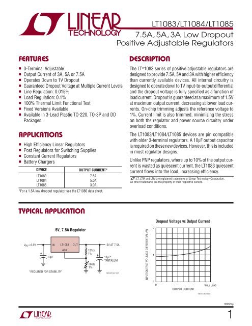
TYPICAL APPLICATION<br />
7.5A<br />
5.0A<br />
3.0A<br />
*For a 1.5A low dropout regulator see the LT1086 data sheet.<br />
V IN ≥ 6.5V<br />
+<br />
10μF<br />
*REQUIRED FOR STABILITY<br />
5V, 7.5A Regulator<br />
IN <strong>LT1083</strong><br />
ADJ<br />
OUT<br />
121Ω<br />
1%<br />
365Ω<br />
1%<br />
+<br />
5V AT 7.5A<br />
10μF*<br />
TANTALUM<br />
1083/4/5 ADJ TA01<br />
DESCRIPTION<br />
<strong>LT1083</strong>/<strong>LT1084</strong>/<strong>LT1085</strong><br />
7.5A, 5A, 3A Low Dropout<br />
Positive Adjustable Regulators<br />
The LT ® 1083 series of positive adjustable regulators are<br />
designed to provide 7.5A, 5A and 3A with higher effi ciency<br />
than currently available devices. All internal circuitry is<br />
designed to operate down to 1V input-to-output differential<br />
and the dropout voltage is fully specifi ed as a function of<br />
load current. Dropout is guaranteed at a maximum of 1.5V<br />
at maximum output current, decreasing at lower load currents.<br />
On-chip trimming adjusts the reference voltage to<br />
1%. Current limit is also trimmed, minimizing the stress<br />
on both the regulator and power source circuitry under<br />
overload conditions.<br />
The <strong>LT1083</strong>/<strong>LT1084</strong>/<strong>LT1085</strong> devices are pin compatible<br />
with older 3-terminal regulators. A 10μF output capacitor<br />
is required on these new devices. However, this is included<br />
in most regulator designs.<br />
Unlike PNP regulators, where up to 10% of the output current<br />
is wasted as quiescent current, the <strong>LT1083</strong> quiescent<br />
current fl ows into the load, increasing effi ciency.<br />
, LT, LTM and LTM are registered trademarks of <strong>Linear</strong> <strong>Technology</strong> Corporation.<br />
All other trademarks are the property of their respective owners.<br />
INPUT/OUTPUT VOLTAGE DIFFERENTIAL (V)<br />
2<br />
1<br />
0<br />
0<br />
Dropout Voltage vs Output Current<br />
OUTPUT CURRENT<br />
1083/4/5 ADJ TA02<br />
IFULL LOAD<br />
108345fg<br />
1
<strong>LT1083</strong>/<strong>LT1084</strong>/<strong>LT1085</strong><br />
ABSOLUTE MAXIMUM RATINGS<br />
Power Dissipation ................................Internally Limited<br />
Input-to-Output Voltage Differential<br />
C-Grades ..............................................................30V<br />
I-Grades ................................................................30V<br />
M-Grades (OBSOLETE) .........................................35V<br />
Operating Junction Temperature Range (Note 9)<br />
C-Grades: Control Section .................. 0°C to 125°C<br />
Power Transistor ................ 0°C to 150°C<br />
I-Grades: Control Section ..............– 40°C to 125°C<br />
Power Transistor ............– 40°C to 150°C<br />
PIN CONFIGURATION<br />
2<br />
TAB<br />
IS<br />
OUTPUT<br />
V IN<br />
ADJ<br />
FRONT VIEW<br />
T PACKAGE<br />
3-LEAD PLASTIC TO-220<br />
3<br />
2<br />
1<br />
θ JA = 50°C/W<br />
BOTTOM VIEW<br />
2<br />
1<br />
CASE IS<br />
OUTPUT<br />
K PACKAGE<br />
2-LEAD TO-3 METAL CAN<br />
θJA = 35°C/W<br />
OBSOLETE PACKAGE<br />
VIN<br />
V OUT<br />
ADJ<br />
(Note 1)<br />
M-Grades: (OBSOLETE)<br />
Control Section ..............– 55°C to 150°C<br />
Power Transistor ............ –55°C to 200°C<br />
Storage Temperature Range ...................–65°C to 150°C<br />
Lead Temperature (Soldering, 10 sec) .................. 300°C<br />
PRECONDITIONING<br />
100% thermal shutdown functional test.<br />
TAB IS<br />
OUTPUT<br />
TAB<br />
IS<br />
OUTPUT<br />
FRONT VIEW<br />
3<br />
2<br />
1<br />
P PACKAGE<br />
3-LEAD PLASTIC TO-3P<br />
θJA = 35°C/W<br />
FRONT VIEW<br />
3<br />
2<br />
1<br />
V IN<br />
V OUT<br />
ADJ<br />
V IN<br />
V OUT<br />
ADJ<br />
M PACKAGE<br />
3-LEAD PLASTIC DD<br />
θJA = 30°C/W*<br />
*WITH PACKAGE SOLDERED TO 0.5IN2 COPPER AREA OVER<br />
BACKSIDE GROUND PLANE OR INTERNAL POWER PLANE. θJA CAN VARY<br />
FROM 20°C/W TO >40°C/W DEPENDING ON MOUNTING TECHNIQUE<br />
108345fg
ORDER INFORMATION<br />
<strong>LT1083</strong>/<strong>LT1084</strong>/<strong>LT1085</strong><br />
LEAD FREE FINISH TAPE AND REEL PART MARKING* PACKAGE DESCRIPTION TEMPERATURE RANGE<br />
<strong>LT1083</strong>CP#PBF <strong>LT1083</strong>CP#TRPBF <strong>LT1083</strong>CP 3-Lead Plastic TO-3P Control: 0°C to 125°C<br />
Power: 0°C to 150°C<br />
<strong>LT1084</strong>CP#PBF <strong>LT1084</strong>CP#TRPBF <strong>LT1084</strong>CP 3-Lead Plastic TO-3P Control: 0°C to 125°C<br />
Power: 0°C to 150°C<br />
<strong>LT1084</strong>CT#PBF <strong>LT1084</strong>CT#TRPBF <strong>LT1084</strong>CT 3-Lead Plastic TO-220 Control: 0°C to 125°C<br />
Power: 0°C to 150°C<br />
<strong>LT1084</strong>IT#PBF <strong>LT1084</strong>IT#TRPBF <strong>LT1084</strong>IT 3-Lead Plastic TO-220 Control: –40°C to 125°C<br />
Power: –40°C to 150°C<br />
<strong>LT1085</strong>CT#PBF <strong>LT1085</strong>CT#TRPBF <strong>LT1085</strong>CT 3-Lead Plastic TO-220 Control: 0°C to 125°C<br />
Power: 0°C to 150°C<br />
<strong>LT1085</strong>IT#PBF <strong>LT1085</strong>IT#TRPBF <strong>LT1085</strong>IT 3-Lead Plastic TO-220 Control: –40°C to 125°C<br />
Power: –40°C to 150°C<br />
<strong>LT1085</strong>CM#PBF <strong>LT1085</strong>CM#TRPBF <strong>LT1085</strong>CM 3-Lead Plastic DD Control: 0°C to 125°C<br />
Power: 0°C to 150°C<br />
<strong>LT1085</strong>IM#PBF <strong>LT1085</strong>IM#TRPBF <strong>LT1085</strong>IM 3-Lead Plastic DD Control: –40°C to 125°C<br />
Power: –40°C to 150°C<br />
LEAD BASED FINISH TAPE AND REEL PART MARKING* PACKAGE DESCRIPTION TEMPERATURE RANGE<br />
<strong>LT1083</strong>CP <strong>LT1083</strong>CP#TR <strong>LT1083</strong>CP 3-Lead Plastic TO-3P Control: 0°C to 125°C<br />
Power: 0°C to 150°C<br />
<strong>LT1084</strong>CP <strong>LT1084</strong>CP#TR <strong>LT1084</strong>CP 3-Lead Plastic TO-3P Control: 0°C to 125°C<br />
Power: 0°C to 150°C<br />
<strong>LT1084</strong>CT <strong>LT1084</strong>CT#TR <strong>LT1084</strong>CT 3-Lead Plastic TO-220 Control: 0°C to 125°C<br />
Power: 0°C to 150°C<br />
<strong>LT1084</strong>IT <strong>LT1084</strong>IT#TR <strong>LT1084</strong>IT 3-Lead Plastic TO-220 Control: –40°C to 125°C<br />
Power: –40°C to 150°C<br />
<strong>LT1085</strong>CT <strong>LT1085</strong>CT#TR <strong>LT1085</strong>CT 3-Lead Plastic TO-220 Control: 0°C to 125°C<br />
Power: 0°C to 150°C<br />
<strong>LT1085</strong>IT <strong>LT1085</strong>IT#TR <strong>LT1085</strong>IT 3-Lead Plastic TO-220 Control: –40°C to 125°C<br />
Power: –40°C to 150°C<br />
<strong>LT1085</strong>CM <strong>LT1085</strong>CM#TR <strong>LT1085</strong>CM 3-Lead Plastic DD Control: 0°C to 125°C<br />
Power: 0°C to 150°C<br />
<strong>LT1085</strong>IM <strong>LT1085</strong>IM#TR <strong>LT1085</strong>IM 3-Lead Plastic DD Control: –40°C to 125°C<br />
Power: –40°C to 150°C<br />
<strong>LT1083</strong>CK <strong>LT1083</strong>CK#TR <strong>LT1083</strong>CK 2-Lead TO-3 Metal Can Control: 0°C to 125°C<br />
Power: 0°C to 150°C<br />
<strong>LT1083</strong>MK <strong>LT1083</strong>MK#TR <strong>LT1083</strong>MK 2-Lead TO-3 Metal Can Control: –55°C to 150°C<br />
Power: –55°C to 200°C<br />
<strong>LT1084</strong>CK <strong>LT1084</strong>CK#TR <strong>LT1084</strong>CK 2-Lead TO-3 Metal Can Control: 0°C to 125°C<br />
Power: 0°C to 150°C<br />
<strong>LT1084</strong>MK <strong>LT1084</strong>MK#TR <strong>LT1084</strong>MK 2-Lead TO-3 Metal Can Control: –55°C to 150°C<br />
Power: –55°C to 200°C<br />
<strong>LT1085</strong>CK <strong>LT1085</strong>CK#TR <strong>LT1085</strong>CK 2-Lead TO-3 Metal Can Control: 0°C to 125°C<br />
Power: 0°C to 150°C<br />
<strong>LT1085</strong>MK <strong>LT1085</strong>MK#TR <strong>LT1085</strong>MK 2-Lead TO-3 Metal Can Control: –55°C to 150°C<br />
Power: –55°C to 200°C<br />
OBSOLETE PACKAGE<br />
Consult LTC Marketing for parts specifi ed with wider operating temperature ranges. *The temperature grade is identifi ed by a label on the shipping container.<br />
For more information on lead free part marking, go to: http://www.linear.com/leadfree/<br />
For more information on tape and reel specifi cations, go to: http://www.linear.com/tapeandreel/<br />
108345fg<br />
3
<strong>LT1083</strong>/<strong>LT1084</strong>/<strong>LT1085</strong><br />
ELECTRICAL CHARACTERISTICS<br />
The l denotes the specifi cations which apply over the full operating<br />
temperature range, otherwise specifi cations are at TA = 25°C.<br />
PARAMETER CONDITIONS MIN TYP MAX UNITS<br />
Reference Voltage IOUT = 10mA, TJ = 25°C,<br />
(VIN – VOUT) = 3V<br />
10mA ≤ IOUT ≤ IFULL_LOAD<br />
1.5V ≤ (VIN – VOUT) ≤ 25V (Notes 4, 6, 7) l<br />
1.238<br />
1.225<br />
1.250<br />
1.250<br />
1.262<br />
1.270<br />
V<br />
V<br />
Line Regulation ILOAD = 10mA, 1.5V ≤ (VIN – VOUT) ≤ 15V, TJ = 25°C (Notes 2, 3)<br />
l<br />
0.015<br />
0.035<br />
0.2<br />
0.2<br />
%<br />
%<br />
M-Grade: 15V ≤ (VIN – VOUT) ≤ 35V (Notes 2, 3) l 0.05 0.5 %<br />
C-, I-Grades: 15V ≤ (VIN – VOUT) ≤ 30V (Notes 2, 3) l 0.05 0.5 %<br />
Load Regulation (VIN – VOUT) = 3V, 10mA ≤ IOUT ≤ IFULL_LOAD, TJ = 25°C<br />
(Notes 2, 3, 4, 6) l<br />
0.1<br />
0.2<br />
0.3<br />
0.4<br />
%<br />
%<br />
Dropout Voltage<br />
Current Limit<br />
ΔVREF = 1%, IOUT = IFULL_LOAD (Notes 5, 6, 8) l 1.3 1.5 V<br />
<strong>LT1083</strong><br />
<strong>LT1084</strong><br />
<strong>LT1085</strong><br />
(VIN – VOUT) = 5V<br />
(VIN – VOUT) = 25V<br />
(VIN – VOUT) = 5V<br />
(VIN – VOUT) = 25V<br />
(VIN – VOUT) = 5V<br />
(VIN – VOUT) = 25V<br />
l<br />
l<br />
l<br />
l<br />
l<br />
l<br />
8.0<br />
0.4<br />
5.5<br />
0.3<br />
3.2<br />
0.2<br />
9.5<br />
1.0<br />
6.5<br />
0.6<br />
4.0<br />
0.5<br />
A<br />
A<br />
A<br />
A<br />
A<br />
A<br />
Minimum Load Current (VIN – VOUT) = 25V l 5 10 mA<br />
Thermal Regulation<br />
<strong>LT1083</strong><br />
TA = 25°C, 30ms Pulse<br />
0.002 0.010 %/W<br />
<strong>LT1084</strong><br />
0.003 0.015 %/W<br />
<strong>LT1085</strong><br />
0.004 0.020 %/W<br />
Ripple Rejection f = 120Hz, CADJ = 25μF, COUT = 25μF Tantalum<br />
IOUT = IFULL_LOAD, (VIN – VOUT) = 3V (Notes 6, 7, 8)<br />
l 60 75 dB<br />
Adjust Pin Current TJ = 25°C<br />
l<br />
55<br />
120<br />
μA<br />
μA<br />
Adjust Pin Current Change 10mA ≤ IOUT ≤ IFULL_LOAD, 1.5V ≤ (VIN – VOUT) ≤ 25V (Note 6) l 0.2 5 μA<br />
Temperature Stability l 0.5 %<br />
Long-Term Stability TA = 125°C, 1000 Hrs 0.3 1 %<br />
RMS Output Noise (% of VOUT) TA = 25°C, 10Hz = ≤ f ≤ 10kHz 0.003 %<br />
4<br />
108345fg
ELECTRICAL CHARACTERISTICS<br />
Note 1: Stresses beyond those listed under Absolute Maximum Ratings<br />
may cause permanent damage to the device. Exposure to any Absolute<br />
Maximum Rating condition for extended periods may affect device<br />
reliability and lifetime.<br />
Note 2: See thermal regulation specifi cations for changes in output voltage<br />
due to heating effects. Load and line regulation are measured at a constant<br />
junction temperature by low duty cycle pulse testing.<br />
Note 3: Line and load regulation are guaranteed up to the maximum power<br />
dissipation (60W for the <strong>LT1083</strong>, 45W for the <strong>LT1084</strong> (K, P), 30W for the<br />
<strong>LT1084</strong> (T) and 30W for the <strong>LT1085</strong>). Power dissipation is determined by<br />
the input/output differential and the output current. Guaranteed maximum<br />
power dissipation will not be available over the full input/output voltage<br />
range.<br />
Note 4: I FULL_LOAD is defi ned in the current limit curves. The I FULL_LOAD<br />
curve is defi ned as the minimum value of current limit as a function of<br />
input-to-output voltage. Note that the 60W power dissipation for the<br />
<strong>LT1083</strong> (45W for the <strong>LT1084</strong> (K, P), 30W for the <strong>LT1084</strong> (T), 30W for the<br />
<strong>LT1085</strong>) is only achievable over a limited range of input-to-output voltage.<br />
<strong>LT1083</strong>/<strong>LT1084</strong>/<strong>LT1085</strong><br />
The l denotes the specifi cations which apply over the full operating<br />
temperature range, otherwise specifi cations are at TA = 25°C.<br />
PARAMETER CONDITIONS MIN TYP MAX UNITS<br />
Thermal Resistance Junction-to-Case<br />
<strong>LT1083</strong><br />
<strong>LT1084</strong><br />
<strong>LT1085</strong><br />
Control Circuitry/Power Transistor<br />
K Package<br />
P Package<br />
K Package<br />
P Package<br />
T Package<br />
K Package<br />
M, T Package<br />
0.6/1.6<br />
0.5/1.6<br />
0.75/2.3<br />
0.65/2.3<br />
0.65/2.7<br />
0.9/3.0<br />
0.7/3.0<br />
°C/W<br />
°C/W<br />
°C/W<br />
°C/W<br />
°C/W<br />
°C/W<br />
°C/W<br />
Note 5: Dropout voltage is specifi ed over the full output current range of<br />
the device. Test points and limits are shown on the Dropout Voltage<br />
curve.<br />
Note 6: For <strong>LT1083</strong> I FULL_LOAD is 5A for –55°C ≤ TJ < – 40°C and 7.5A for<br />
T J ≥ –40°C.<br />
Note 7: 1.7V ≤ (V IN – V OUT) ≤ 25V for <strong>LT1084</strong> at –55°C ≤ T J ≤ – 40°C.<br />
Note 8: Dropout is 1.7V maximum for <strong>LT1084</strong> at –55°C ≤ T J ≤ –40°C.<br />
Note 9: The <strong>LT1083</strong>/<strong>LT1084</strong>/<strong>LT1085</strong> regulators are tested and specifi ed<br />
under pulse load conditions such that T J ≅ T A. The C-grade <strong>LT1083</strong>/<br />
<strong>LT1084</strong>/<strong>LT1085</strong> are 100% tested at 25°C.The I-grade <strong>LT1084</strong>/<strong>LT1085</strong> are<br />
guaranteed over the full –40°C to 125°C operating ambient temperature<br />
range.<br />
108345fg<br />
5
<strong>LT1083</strong>/<strong>LT1084</strong>/<strong>LT1085</strong><br />
TYPICAL PERFORMANCE CHARACTERISTICS<br />
MINIMUM INPUT/OUTPUT DIFFERENTIAL (V)<br />
MINIMUN INPUT/OUTPUT DIFFERENTIAL (V)<br />
MINIMUM INPUT/OUTPUT DIFFERENTIAL (V)<br />
6<br />
2<br />
1<br />
0<br />
0<br />
2<br />
1<br />
0<br />
0<br />
2<br />
1<br />
<strong>LT1083</strong><br />
Dropout Voltage<br />
INDICATES GUARANTEED TEST POINT<br />
0°C ≤ T J ≤ 125°C<br />
–40°C ≤ T J ≤ 150°C<br />
T J = 150°C<br />
T J = 25°C<br />
T J = –55°C<br />
1 2 3 4 5 6 7 8 9 10<br />
<strong>LT1084</strong><br />
Dropout Voltage<br />
OUTPUT CURRENT (A)<br />
<strong>LT1083</strong>/4/5 ADJ G01<br />
INDICATES GUARANTEED TEST POINT<br />
0°C ≤ T J ≤ 125°C<br />
T J = 150°C<br />
–55°C ≤ T J ≤ 150°C<br />
T J = 25°C<br />
1 2 3 4<br />
OUTPUT CURRENT (A)<br />
<strong>LT1085</strong><br />
Dropout Voltage<br />
0<br />
0<br />
T J = –55°C<br />
<strong>LT1083</strong>/4/5 ADJ G04<br />
INDICATES GUARANTEED TEST POINT<br />
0°C ≤ T J ≤ 125°C<br />
T J = 150°C<br />
–55°C ≤ T J ≤ 150°C<br />
T J = 25°C<br />
5<br />
T J = –55°C<br />
1 2 3 4<br />
OUTPUT CURRENT (A)<br />
<strong>LT1083</strong>/4/5 ADJ G07<br />
6<br />
SHORT-CIRCUIT CURRENT (A)<br />
SHORT-CIRCUIT CURRENT (A)<br />
SHORT-CIRCUIT CURRENT (A)<br />
12<br />
10<br />
8<br />
6<br />
4<br />
2<br />
0<br />
0<br />
10<br />
9<br />
8<br />
7<br />
6<br />
5<br />
4<br />
3<br />
2<br />
1<br />
0<br />
0<br />
6<br />
5<br />
4<br />
3<br />
2<br />
1<br />
0<br />
0<br />
<strong>LT1083</strong><br />
Short-Circut Current<br />
–55°C<br />
IFULL LOAD<br />
GUARANTEED<br />
25°C<br />
150°C<br />
5 10 15 20 25 30 35<br />
INPUT/OUTPUT DIFFERENTIAL (V)<br />
<strong>LT1084</strong><br />
Short-Circut Current<br />
IFULL LOAD<br />
GUARANTEED<br />
150°C<br />
25°C<br />
–55°C<br />
<strong>LT1083</strong>/4/5 ADJ G02<br />
5 10 15 20 25 30 35<br />
INPUT/OUTPUT DIFFERENTIAL (V)<br />
<strong>LT1085</strong><br />
Short-Circuit Current<br />
–55°C<br />
IFULL LOAD<br />
GUARANTEED<br />
25°C<br />
150°C<br />
<strong>LT1083</strong>/4/5 ADJ G05<br />
5 10 15 20 25 30 35<br />
INPUT/OUTPUT DIFFERENTIAL (V)<br />
<strong>LT1083</strong>/4/5 ADJ G08<br />
OUTPUT VOLTAGE DEVIATION (%)<br />
OUTPUT VOLTAGE DEVIATION (%)<br />
OUTPUT VOLTAGE DEVIATION (%)<br />
0.10<br />
0.05<br />
0<br />
–0.05<br />
–0.10<br />
–0.15<br />
–0.20<br />
–50<br />
0.10<br />
0.05<br />
0<br />
–0.05<br />
–0.10<br />
–0.15<br />
–0.20<br />
–50<br />
0.10<br />
0.05<br />
0<br />
–0.05<br />
–0.10<br />
–0.15<br />
–0.20<br />
–50<br />
<strong>LT1083</strong><br />
Load Regulation<br />
ΔI = 7.5A<br />
–25 0 25 50 75 100 125 150<br />
TEMPERATURE (°C)<br />
<strong>LT1084</strong><br />
Load Regulation<br />
ΔI = 5A<br />
<strong>LT1083</strong>/4/5 ADJ G03<br />
–25 0 25 50 75 100 125 150<br />
TEMPERATURE (°C)<br />
<strong>LT1085</strong><br />
Load Regulation<br />
ΔI = 3A<br />
<strong>LT1083</strong>/4/5 ADJ G06<br />
–25 0 25 50 75 100 125 150<br />
TEMPERATURE (°C)<br />
<strong>LT1083</strong>/4/5 ADJ G09<br />
108345fg
TYPICAL PERFORMANCE CHARACTERISTICS<br />
MINIMUM OPERATING CURRENT (mA)<br />
RIPPLE REJECTION (dB)<br />
RIPPLE REJECTION (dB)<br />
10<br />
9<br />
8<br />
7<br />
6<br />
5<br />
4<br />
3<br />
2<br />
1<br />
0<br />
0<br />
100<br />
90<br />
80<br />
70<br />
60<br />
50<br />
40<br />
30<br />
20<br />
10<br />
T J = 25°C<br />
T J = –55°C<br />
T J = 150°C<br />
5 10 15 20 25 30 35<br />
INPUT/OUTPUT DIFFERENTIAL (V)<br />
V RIPPLE ≤ 3V P-P<br />
(V IN – V OUT) ≥ V DROPOUT<br />
<strong>LT1083</strong>/4/5 ADJ G10<br />
V RIPPLE<br />
≤ 0.5V P-P<br />
(V IN – V OUT) ≥ 3V<br />
C ADJ = 200μF AT FREQUENCIES < 60Hz<br />
CADJ = 25μF AT FREQUENCIES > 60Hz<br />
IOUT = 7A<br />
0<br />
10 100 1k<br />
FREQUENCY (Hz)<br />
10k 100k<br />
100<br />
90<br />
80<br />
70<br />
60<br />
50<br />
40<br />
30<br />
20<br />
10<br />
V RIPPLE ≤ 3V P-P<br />
(V IN – V OUT) ≥ V DROPOUT<br />
1083/4/5 ADJ G13<br />
V RIPPLE ≤ 0.5V P-P<br />
(V IN – V OUT) ≥ 3V<br />
C ADJ = 200μF AT FREQUENCIES < 60Hz<br />
CADJ = 25μF AT FREQUENCIES > 60Hz<br />
IOUT = 5A<br />
0<br />
10 100 1k<br />
FREQUENCY (Hz)<br />
10k 100k<br />
1083/4/5 ADJ G16<br />
REFERENCE VOLTAGE (V)<br />
RIPPLE REJECTION (dB)<br />
RIPPLE REJECTION (dB)<br />
1.27<br />
1.26<br />
1.25<br />
1.24<br />
1.23<br />
–50 –25 0 25 50 75 100 125 150<br />
TEMPERATURE (°C)<br />
100<br />
90<br />
80<br />
70<br />
60<br />
50<br />
40<br />
30<br />
20<br />
10<br />
0<br />
0<br />
100<br />
90<br />
80<br />
70<br />
60<br />
50<br />
40<br />
30<br />
20<br />
10<br />
0<br />
0<br />
f R = 20kHz<br />
VRIPPLE ≤ 0.5V P-P<br />
V OUT = 5V<br />
CADJ = 25μF<br />
COUT = 25μF<br />
<strong>LT1083</strong>/4/5 ADJ G11<br />
f R = 120Hz<br />
VRIPPLE ≤ 3V P-P<br />
1 2 3 4 5 6 7 8<br />
OUTPUT CURRENT (A)<br />
1083/4/5 ADJ G14<br />
1 2 3 4 5<br />
OUTPUT CURRENT (A)<br />
<strong>LT1083</strong>/<strong>LT1084</strong>/<strong>LT1085</strong><br />
Minimum Operating Current Temperature Stability Adjust Pin Current<br />
<strong>LT1083</strong><br />
Ripple Rejection<br />
<strong>LT1084</strong><br />
Ripple Rejection<br />
<strong>LT1083</strong><br />
Ripple Rejection vs Current<br />
<strong>LT1084</strong><br />
Ripple Rejection vs Current<br />
f R = 20kHz<br />
VRIPPLE ≤ 0.5V P-P<br />
V OUT = 5V<br />
CADJ = 25μF<br />
COUT = 25μF<br />
f R = 120Hz<br />
VRIPPLE ≤ 3V P-P<br />
1083/4/5 ADJ G17<br />
ADJUST PIN CURRENT (μA)<br />
POWER (W)<br />
POWER (W)<br />
100<br />
90<br />
80<br />
70<br />
60<br />
50<br />
40<br />
30<br />
20<br />
10<br />
0<br />
–50 –25 0 25 50 75 100 125 150<br />
TEMPERATURE (°C)<br />
<strong>LT1083</strong>/4/5 ADJ G12<br />
100<br />
90<br />
80<br />
70<br />
60<br />
50<br />
40<br />
<strong>LT1083</strong>MK<br />
30<br />
20<br />
<strong>LT1083</strong>CP<br />
10<br />
<strong>LT1083</strong>CK<br />
0<br />
50 60 70 80 90 100 110 120 130 140 150<br />
CASE TEMPERATURE (°C)<br />
* AS LIMITED BY MAXIMUM JUNCTION TEMPERATURE<br />
60<br />
50<br />
40<br />
30<br />
20<br />
10<br />
<strong>LT1083</strong><br />
Maximum Power Dissipation*<br />
<strong>LT1084</strong><br />
Maximum Power Dissipation*<br />
<strong>LT1084</strong>CT<br />
<strong>LT1084</strong>CK<br />
<strong>LT1084</strong>MK<br />
<strong>LT1084</strong>CP<br />
<strong>LT1083</strong>/4/5 ADJ G15<br />
0<br />
50 60 70 80 90 100 110 120 130 140 150<br />
CASE TEMPERATURE (°C)<br />
* AS LIMITED BY MAXIMUM JUNCTION TEMPERATURE<br />
<strong>LT1083</strong>/4/5 ADJ G18<br />
108345fg<br />
7
<strong>LT1083</strong>/<strong>LT1084</strong>/<strong>LT1085</strong><br />
TYPICAL PERFORMANCE CHARACTERISTICS<br />
RIPPLE REJECTION (dB)<br />
OUTPUT VOLTAGE<br />
DEVIATION (V)<br />
LOAD CURRENT (A)<br />
OUTPUT VOLTAGE<br />
DEVIATION (mV)<br />
INPUT<br />
DEVIATION (V)<br />
100<br />
90<br />
80<br />
70<br />
60<br />
50<br />
40<br />
30<br />
20<br />
10<br />
8<br />
V RIPPLE ≤ 3V P-P<br />
(V IN – V OUT) ≥ V DROPOUT<br />
V RIPPLE<br />
≤ 0.5V P-P<br />
(V IN – V OUT) ≥ 3V<br />
C ADJ = 200μF AT FREQUENCIES < 60Hz<br />
CADJ = 25μF AT FREQUENCIES > 60Hz<br />
IOUT = 3A<br />
0<br />
10 100 1k<br />
FREQUENCY (Hz)<br />
10k 100k<br />
0.6<br />
0.4<br />
0.2<br />
0<br />
–0.2<br />
–0.4<br />
8<br />
6<br />
4<br />
2<br />
0<br />
0<br />
150<br />
100<br />
50<br />
0<br />
–50<br />
–100<br />
–150<br />
14<br />
13<br />
12<br />
<strong>LT1085</strong><br />
Ripple Rejection<br />
<strong>LT1083</strong><br />
Load Transient Response<br />
CADJ = 0<br />
50<br />
TIME (μs)<br />
1083/4/5 ADJ G19<br />
C ADJ = 1μF<br />
CIN = 1μF<br />
C OUT = 10μF TANTALUM<br />
<strong>LT1083</strong><br />
Line Transient Response<br />
0<br />
C ADJ = 0<br />
100<br />
TIME (μs)<br />
VOUT=10V<br />
V IN=13V<br />
PRELOAD=100mA<br />
1083/4/5 ADJ G22<br />
C ADJ = 1μF<br />
VOUT = 10V<br />
I IN = 0.2A<br />
CIN = 1μF TANTALUM<br />
C OUT = 10μF TANTALUM<br />
1083/4/5 ADJ G25<br />
100<br />
200<br />
RIPPLE REJECTION (dB)<br />
OUTPUT VOLTAGE<br />
DEVIATION (V)<br />
LOAD CURRENT (A)<br />
OUTPUT VOLTAGE<br />
DEVIATION (mV)<br />
INPUT<br />
DEVIATION (V)<br />
100<br />
90<br />
80<br />
70<br />
60<br />
50<br />
40<br />
30<br />
20<br />
10<br />
0<br />
0<br />
0.6<br />
0.4<br />
0.2<br />
0<br />
–0.2<br />
–0.4<br />
–0.6<br />
6<br />
4<br />
2<br />
0<br />
0<br />
60<br />
40<br />
20<br />
0<br />
–20<br />
–40<br />
–60<br />
14<br />
13<br />
12<br />
<strong>LT1085</strong><br />
Ripple Rejection vs Current<br />
f R = 120Hz<br />
VRIPPLE ≤ 3V P-P<br />
0<br />
f R = 20kHz<br />
VRIPPLE ≤ 0.5V P-P<br />
V OUT = 5V<br />
CADJ = 25μF<br />
COUT = 25μF<br />
0.5 1.0 1.5 2.0 2.5 3.0<br />
OUTPUT CURRENT (A)<br />
<strong>LT1084</strong><br />
Load Transient Response<br />
C ADJ = 0<br />
C ADJ = 0<br />
C IN = 1μF<br />
C OUT = 10μF TANTALUM<br />
50<br />
TIME (μs)<br />
<strong>LT1084</strong><br />
Line Transient Response<br />
C ADJ = 1μF<br />
100<br />
TIME (μs)<br />
1083/4/5 ADJ G20<br />
C ADJ = 1μF<br />
V OUT=10V<br />
VIN=13V<br />
PRELOAD=100mA<br />
1083/4/5 ADJ G23<br />
VOUT = 10V<br />
I IN = 0.2A<br />
CIN = 1μF TANTALUM<br />
C OUT = 10μF TANTALUM<br />
1083/4/5 ADJ G26<br />
100<br />
200<br />
POWER (W)<br />
OUTPUT VOLTAGE<br />
DEVIATION (V)<br />
LOAD CURRENT (A)<br />
OUTPUT VOLTAGE<br />
DEVIATION (mV)<br />
INPUT<br />
DEVIATION (V)<br />
50<br />
40<br />
30<br />
20<br />
10<br />
0<br />
50 60 70 80 90 100 110 120 130 140 150<br />
CASE TEMPERATURE (°C)<br />
* AS LIMITED BY MAXIMUM JUNCTION TEMPERATURE<br />
0.3<br />
0.2<br />
0.1<br />
0<br />
–0.1<br />
–0.2<br />
–0.3<br />
3<br />
2<br />
1<br />
0<br />
0<br />
60<br />
40<br />
20<br />
0<br />
–20<br />
–40<br />
–60<br />
14<br />
13<br />
12<br />
<strong>LT1085</strong><br />
Maximum Power Dissipation*<br />
0<br />
C ADJ = 0<br />
<strong>LT1085</strong>MK<br />
<strong>LT1085</strong>CK<br />
C ADJ = 0<br />
CIN = 1μF<br />
C OUT = 10μF TANTALUM<br />
50<br />
TIME (μs)<br />
100<br />
TIME (μs)<br />
<strong>LT1085</strong>CT<br />
<strong>LT1085</strong><br />
Load Transient Response<br />
<strong>LT1085</strong><br />
Line Transient Response<br />
<strong>LT1083</strong>/4/5 ADJ G21<br />
C ADJ = 1μF<br />
V OUT=10V<br />
V IN=13V<br />
PRELOAD=100mA<br />
1083/4/5 ADJ G24<br />
CADJ = 1μF<br />
VOUT = 10V<br />
I IN = 0.2A<br />
CIN = 1μF TANTALUM<br />
C OUT = 10μF TANTALUM<br />
1083/4/5 ADJ G27<br />
100<br />
200<br />
108345fg
BLOCK DIAGRAM<br />
VADJ<br />
THERMAL<br />
LIMIT<br />
APPLICATIONS INFORMATION<br />
The <strong>LT1083</strong> family of 3-terminal adjustable regulators is<br />
easy to use and has all the protection features that are<br />
expected in high performance voltage regulators. They are<br />
short-circuit protected, and have safe area protection as<br />
well as thermal shutdown to turn off the regulator should<br />
the junction temperature exceed about 165°C.<br />
These regulators are pin compatible with older 3-terminal<br />
adjustable devices, offer lower dropout voltage and more<br />
precise reference tolerance. Further, the reference stability<br />
with temperature is improved over older types of regulators.<br />
The only circuit difference between using the <strong>LT1083</strong><br />
family and older regulators is that this new family requires<br />
an output capacitor for stability.<br />
Stability<br />
The circuit design used in the <strong>LT1083</strong> family requires the<br />
use of an output capacitor as part of the device frequency<br />
compensation. For all operating conditions, the addition of<br />
a 150μF aluminium electrolytic or a 22μF solid tantalum<br />
V IN<br />
<strong>LT1083</strong>/<strong>LT1084</strong>/<strong>LT1085</strong><br />
V OUT<br />
+<br />
–<br />
1083/4/5 ADJ BD<br />
on the output will ensure stability. Normally, capacitors<br />
much smaller than this can be used with the <strong>LT1083</strong>. Many<br />
different types of capacitors with widely varying characteristics<br />
are available. These capacitors differ in capacitor<br />
tolerance (sometimes ranging up to ±100%), equivalent<br />
series resistance, and capacitance temperature coeffi cient.<br />
The 150μF or 22μF values given will ensure stability.<br />
When the adjustment terminal is bypassed to improve the<br />
ripple rejection, the requirement for an output capacitor<br />
increases. The value of 22μF tantalum or 150μF aluminum<br />
covers all cases of bypassing the adjustment terminal.<br />
Without bypassing the adjustment terminal, smaller<br />
capacitors can be used with equally good results and the<br />
table below shows approximately what size capacitors are<br />
needed to ensure stability.<br />
Recommended Capacitor Values<br />
INPUT OUTPUT ADJUSTMENT<br />
10μF<br />
10μF<br />
10μF Tantalum, 50μF Aluminum<br />
22μF Tantalum, 150μF Aluminum<br />
None<br />
20μF<br />
108345fg<br />
9
<strong>LT1083</strong>/<strong>LT1084</strong>/<strong>LT1085</strong><br />
APPLICATIONS INFORMATION<br />
Normally, capacitor values on the order of 100μF are used<br />
in the output of many regulators to ensure good transient<br />
response with heavy load current changes. Output capacitance<br />
can be increased without limit and larger values of<br />
output capacitor further improve stability and transient<br />
response of the <strong>LT1083</strong> regulators.<br />
Another possible stability problem that can occur in monolithic<br />
IC regulators is current limit oscillations. These can<br />
occur because, in current limit, the safe area protection<br />
exhibits a negative impedance. The safe area protection<br />
decreases the current limit as the input-to-output voltage<br />
increases. That is the equivalent of having a negative<br />
resistance since increasing voltage causes current to<br />
decrease. Negative resistance during current limit is not<br />
unique to the <strong>LT1083</strong> series and has been present on all<br />
power IC regulators. The value of the negative resistance<br />
is a function of how fast the current limit is folded back as<br />
input-to-output voltage increases. This negative resistance<br />
can react with capacitors or inductors on the input to cause<br />
oscillation during current limiting. Depending on the value<br />
of series resistance, the overall circuitry may end up unstable.<br />
Since this is a system problem, it is not necessarily<br />
easy to solve; however, it does not cause any problems<br />
with the IC regulator and can usually be ignored.<br />
Protection Diodes<br />
In normal operation, the <strong>LT1083</strong> family does not need<br />
any protection diodes. Older adjustable regulators required<br />
protection diodes between the adjustment pin and<br />
the output and from the output to the input to prevent<br />
overstressing the die. The internal current paths on the<br />
<strong>LT1083</strong> adjustment pin are limited by internal resistors.<br />
Therefore, even with capacitors on the adjustment pin, no<br />
protection diode is needed to ensure device safety under<br />
short-circuit conditions.<br />
Diodes between input and output are usually not needed.<br />
The internal diode between the input and the output pins<br />
of the <strong>LT1083</strong> family can handle microsecond surge currents<br />
of 50A to 100A. Even with large output capacitances,<br />
it is very diffi cult to get those values of surge currents<br />
in normal operations. Only with a high value of output<br />
capacitors, such as 1000μF to 5000μF and with the input<br />
10<br />
pin instantaneously shorted to ground, can damage occur.<br />
A crowbar circuit at the input of the <strong>LT1083</strong> can generate<br />
those kinds of currents, and a diode from output to input is<br />
then recommended. Normal power supply cycling or even<br />
plugging and unplugging in the system will not generate<br />
current large enough to do any damage.<br />
The adjustment pin can be driven on a transient basis<br />
±25V, with respect to the output without any device degradation.<br />
Of course, as with any IC regulator, exceeding<br />
the maximum input to output voltage differential causes<br />
the internal transistors to break down and none of the<br />
protection circuitry is functional.<br />
VIN<br />
D1<br />
1N4002<br />
(OPTIONAL)<br />
IN <strong>LT1083</strong><br />
ADJ<br />
OUT<br />
+<br />
C ADJ<br />
10μF<br />
R1<br />
R2<br />
+<br />
V OUT<br />
C OUT<br />
150μF<br />
1083/4/5 ADJ F00<br />
Overload Recovery<br />
Like any of the IC power regulators, the <strong>LT1083</strong> has safe<br />
area protection. The safe area protection decreases the<br />
current limit as input-to-output voltage increases and<br />
keeps the power transistor inside a safe operating region<br />
for all values of input-to-output voltage. The <strong>LT1083</strong><br />
protection is designed to provide some output current<br />
at all values of input-to-output voltage up to the device<br />
breakdown.<br />
When power is fi rst turned on, as the input voltage rises,<br />
the output follows the input, allowing the regulator to start<br />
up into very heavy loads. During the start-up, as the input<br />
voltage is rising, the input-to-output voltage differential<br />
remains small, allowing the regulator to supply large<br />
output currents. With high input voltage, a problem can<br />
occur wherein removal of an output short will not allow<br />
the output voltage to recover. Older regulators, such as<br />
the 7800 series, also exhibited this phenomenon, so it is<br />
not unique to the <strong>LT1083</strong>.<br />
108345fg
APPLICATIONS INFORMATION<br />
The problem occurs with a heavy output load when the<br />
input voltage is high and the output voltage is low, such<br />
as immediately after removal of a short. The load line for<br />
such a load may intersect the output current curve at two<br />
points. If this happens, there are two stable output operating<br />
points for the regulator. With this double intersection,<br />
the power supply may need to be cycled down to zero and<br />
brought up again to make the output recover.<br />
Ripple Rejection<br />
The typical curves for ripple rejection refl ect values for a<br />
bypassed adjustment pin. This curve will be true for all<br />
values of output voltage. For proper bypassing and ripple<br />
rejection approaching the values shown, the impedance<br />
of the adjust pin capacitor at the ripple frequency should<br />
be less than the value of R1, (normally 100Ω to 120Ω).<br />
The size of the required adjust pin capacitor is a function<br />
of the input ripple frequency. At 120Hz the adjust pin<br />
capacitor should be 25μF if R1 = 100Ω. At 10kHz only<br />
0.22μF is needed.<br />
For circuits without an adjust pin bypass capacitor, the ripple<br />
rejection will be a function of output voltage. The output<br />
ripple will increase directly as a ratio of the output voltage<br />
to the reference voltage (VOUT/VREF). For example, with<br />
the output voltage equal to 5V and no adjust pin capacitor,<br />
the output ripple will be higher by the ratio of 5V/1.25V<br />
or four times larger. Ripple rejection will be degraded by<br />
12dB from the value shown on the typical curve.<br />
Output Voltage<br />
The <strong>LT1083</strong> develops a 1.25V reference voltage between<br />
the output and the adjust terminal (see Figure 1). By<br />
placing a resistor R1 between these two terminals, a<br />
constant current is caused to fl ow through R1 and down<br />
through R2 to set the overall output voltage. Normally this<br />
current is the specifi ed minimum load current of 10mA.<br />
Because IADJ is very small and constant when compared<br />
with the current through R1, it represents a small error<br />
and can usually be ignored.<br />
<strong>LT1083</strong>/<strong>LT1084</strong>/<strong>LT1085</strong><br />
Load Regulation<br />
Because the <strong>LT1083</strong> is a 3-terminal device, it is not possible<br />
to provide true remote load sensing. Load regulation<br />
will be limited by the resistance of the wire connecting<br />
the regulator to the load. The data sheet specifi cation for<br />
load regulation is measured at the bottom of the package.<br />
Negative side sensing is a true Kelvin connection, with the<br />
bottom of the output divider returned to the negative side<br />
of the load. Although it may not be immediately obvious,<br />
best load regulation is obtained when the top of the resistor<br />
divider R1 is connected directly to the case not to the<br />
load. This is illustrated in Figure 2. If R1 were connected<br />
to the load, the effective resistance between the regulator<br />
and the load would be:<br />
R<br />
Figure 1. Basic Adjustable Regulator<br />
⎛ R2+ R1⎞<br />
• , R Parasitic Line<br />
⎝<br />
⎜<br />
R1<br />
⎠<br />
⎟ = Resistance<br />
P P<br />
VIN<br />
VIN<br />
IN <strong>LT1083</strong> OUT<br />
IADJ<br />
50μA<br />
ADJ<br />
VOUT =VREF 1 +<br />
R2<br />
+ IADJ R2<br />
R1<br />
IN<br />
( )<br />
<strong>LT1083</strong> OUT<br />
ADJ<br />
*CONNECT R1 TO CASE<br />
CONNECT R2 TO LOAD<br />
VREF<br />
R1<br />
R2<br />
RP<br />
PARASITIC<br />
LINE RESISTANCE<br />
R1*<br />
R2*<br />
V OUT<br />
1083/4/5 ADJ F01<br />
1083/4/5 ADJ F02<br />
Figure 2. Connections for Best Load Regulation<br />
R L<br />
108345fg<br />
11
<strong>LT1083</strong>/<strong>LT1084</strong>/<strong>LT1085</strong><br />
APPLICATIONS INFORMATION<br />
Connected as shown, RP is not multiplied by the divider<br />
ratio. RP is about 0.004Ω per foot using 16-gauge wire.<br />
This translates to 4mV/ft at 1A load current, so it is important<br />
to keep the positive lead between regulator and<br />
load as short as possible and use large wire or PC board<br />
traces.<br />
Thermal Considerations<br />
The <strong>LT1083</strong> series of regulators have internal power and<br />
thermal limiting circuitry designed to protect the device<br />
under overload conditions. For continuous normal load<br />
conditions however, maximum junction temperature ratings<br />
must not be exceeded. It is important to give careful<br />
consideration to all sources of thermal resistance from<br />
junction to ambient. This includes junction-to-case, caseto-heat<br />
sink interface, and heat sink resistance itself. New<br />
thermal resistance specifi cations have been developed to<br />
more accurately refl ect device temperature and ensure<br />
safe operating temperatures. The data section for these<br />
new regulators provides a separate thermal resistance and<br />
maximum junction temperature for both the Control Section<br />
and the Power Transistor. Previous regulators, with a<br />
single junction-to-case thermal resistance specifi cation,<br />
used an average of the two values provided here and therefore<br />
could allow excessive junction temperatures under<br />
certain conditions of ambient temperature and heat sink<br />
resistance. To avoid this possibility, calculations should<br />
be made for both sections to ensure that both thermal<br />
limits are met.<br />
Junction-to-case thermal resistance is specifi ed from the<br />
IC junction to the bottom of the case directly below the<br />
die. This is the lowest resistance path for heat fl ow. Proper<br />
mounting is required to ensure the best possible thermal<br />
fl ow from this area of the package to the heat sink. Thermal<br />
12<br />
compound at the case-to-heat sink interface is strongly<br />
recommended. If the case of the device must be electrically<br />
isolated, a thermally conductive spacer can be used,<br />
as long as its added contribution to thermal resistance is<br />
considered. Note that the case of all devices in this series<br />
is electrically connected to the output.<br />
For example, using an <strong>LT1083</strong>CK (TO-3, Commercial)<br />
and assuming:<br />
VIN (Max Continuous) = 9V, VOUT = 5V, IOUT = 6A,<br />
TA = 75°C, θHEAT SINK = 1°C/W,<br />
θCASE-TO-HEAT SINK = 0.2°C/W for K package with<br />
thermal compound.<br />
Power dissipation under these conditions is equal to:<br />
PD = (VIN – VOUT )(IOUT) = 24W<br />
Junction temperature will be equal to:<br />
TJ = TA + PD (θHEAT SINK + θCASE-TO-HEAT SINK + θJC) For the Control Section:<br />
TJ = 75°C + 24W (1°C/W + 0.2°C/W + 0.6°C/W) = 118°C<br />
118°C < 125°C = TJMAX (Control Section<br />
Commercial Range)<br />
For the Power Transistor:<br />
TJ = 75°C + 24W (1°C/W + 0.2°C/W + 1.6°C/W) = 142°C<br />
142°C < 150°C = TJMAX (Power Transistor<br />
Commercial Range)<br />
In both cases the junction temperature is below the maximum<br />
rating for the respective sections, ensuring reliable<br />
operation.<br />
108345fg
TYPICAL APPLICATION<br />
110VAC<br />
T1<br />
TRIAD<br />
F-269U<br />
1N4003<br />
C30B<br />
20Ω<br />
20Ω<br />
C30B<br />
1N4003<br />
1μF<br />
1N4148<br />
T2<br />
3<br />
1<br />
560Ω<br />
82k 15k<br />
10k<br />
2<br />
2<br />
3<br />
7<br />
+<br />
–<br />
8<br />
–15V<br />
LT1011<br />
4<br />
L<br />
1mH<br />
1N4003<br />
1<br />
–15V<br />
15V<br />
8<br />
LT1011<br />
*1% FILM RESISTOR<br />
1<br />
L: DALE TO-5 TYPE<br />
T2: STANCOR 11Z-2003<br />
GENERAL PURPOSE REGULATOR WITH SCR PREREGULATOR<br />
TO LOWER POWER DISSIPATION. ABOUT 1.7V DIFFERENTIAL<br />
IS MAINTAINED ACROSS THE <strong>LT1083</strong> INDEPENDENT OF OUTPUT<br />
VOLTAGE AND LOAD CURRENT<br />
4<br />
–<br />
+<br />
2<br />
7.5A Variable Regulator<br />
7<br />
3<br />
15V<br />
+<br />
15V<br />
15K<br />
C1<br />
50,000μF<br />
200k<br />
0.1μF<br />
2N3904<br />
10k<br />
NC<br />
6<br />
15V<br />
1N914<br />
+<br />
–<br />
<strong>LT1083</strong>/<strong>LT1084</strong>/<strong>LT1085</strong><br />
IN<br />
<strong>LT1083</strong><br />
ADJ<br />
OUT<br />
LT1004-1.2<br />
16k*<br />
11k*<br />
100pF<br />
8<br />
LM301A<br />
7<br />
1μF<br />
1<br />
4<br />
–15V<br />
3<br />
2<br />
16k*<br />
11k*<br />
–15V<br />
750Ω*<br />
2k<br />
OUTPUT<br />
ADJUST<br />
LT1004-1.2<br />
2.7k<br />
1.5k<br />
+<br />
0V TO 35V<br />
OA TO 7.5A<br />
100μF<br />
<strong>LT1083</strong>/4/5 ADJ TA05<br />
108345fg<br />
13
<strong>LT1083</strong>/<strong>LT1084</strong>/<strong>LT1085</strong><br />
TYPICAL APPLICATION<br />
14<br />
VIN<br />
RETURN<br />
+<br />
IN<br />
10μF<br />
V IN<br />
V IN<br />
+<br />
IN<br />
IN<br />
10μF<br />
<strong>LT1083</strong> OUT<br />
ADJ<br />
<strong>LT1083</strong><br />
ADJ<br />
Paralleling Regulators<br />
OUT<br />
IN <strong>LT1083</strong><br />
ADJ<br />
OUT<br />
R1<br />
120Ω<br />
*C1 IMPROVES RIPPLE REJECTION.<br />
X C SHOULD BE < R1 AT RIPPLE FREQUENCY<br />
<strong>LT1083</strong> OUT<br />
ADJ<br />
R2<br />
R1<br />
121Ω<br />
1%<br />
Remote Sensing<br />
0.015Ω<br />
Improving Ripple Rejection<br />
121Ω<br />
25Ω<br />
365Ω<br />
+<br />
100μF<br />
R2<br />
365Ω<br />
1%<br />
2 FEET #18 WIRE*<br />
( )<br />
VOUT = 1.25V 1 +<br />
R2<br />
R1<br />
IOUT = 0A TO 15A<br />
*THE #18 WIRE ACTS<br />
AS BALLAST RESISTANCE<br />
INSURING CURRENT SHARING<br />
BETWEEN BOTH DEVICES<br />
+<br />
VIN 7<br />
+<br />
C1<br />
25μF*<br />
R P<br />
(MAX DROP 300mV)<br />
6<br />
1<br />
100pF<br />
LM301A<br />
8<br />
4<br />
–<br />
+<br />
2<br />
3<br />
+<br />
<strong>LT1083</strong>/4/5 ADJ TA03<br />
VOUT<br />
5V<br />
150μF<br />
5μF<br />
25Ω<br />
1083/4/5 ADJ TA04<br />
1k<br />
R L<br />
V OUT<br />
5V<br />
RETURN<br />
1083/4/5 ADJ TA07<br />
108345fg
TYPICAL APPLICATION<br />
V IN<br />
28V<br />
10k<br />
High Effi ciency Regulator with Switching Preregulator<br />
1k<br />
V IN<br />
VIN<br />
TTL<br />
1M<br />
LT1011<br />
+<br />
+<br />
1mH<br />
MR1122<br />
+<br />
–<br />
+<br />
28V<br />
1N914<br />
10,000μF<br />
4N28<br />
10k<br />
10k<br />
470Ω<br />
IN<br />
1N914<br />
28V<br />
1.2V to 15V Adjustable Regulator<br />
C1*<br />
10μF<br />
5V Regulator with Shutdown*<br />
10μF<br />
1k<br />
IN <strong>LT1083</strong><br />
ADJ<br />
OUT<br />
IN<br />
1k<br />
ADJ<br />
R2<br />
1k<br />
<strong>LT1083</strong><br />
2N3904<br />
OUT<br />
*OUTPUT SHUTS DOWN TO 1.3V<br />
R1<br />
90.9Ω<br />
*NEEDED IF DEVICE IS FAR FROM FILTER CAPACITORS<br />
( )<br />
† VOUT = 1.25V 1 + R2<br />
R1<br />
121Ω<br />
1%<br />
365Ω<br />
1%<br />
<strong>LT1083</strong>/<strong>LT1084</strong>/<strong>LT1085</strong><br />
<strong>LT1083</strong> OUT<br />
ADJ<br />
+<br />
+<br />
V OUT †<br />
C2<br />
100μF<br />
1083/4/5 ADJ TA08<br />
VOUT<br />
5V<br />
100μF<br />
1083/4/5 ADJ TA09<br />
1083/4/5 ADJ TA06<br />
240Ω<br />
2k<br />
VOUT<br />
108345fg<br />
15
<strong>LT1083</strong>/<strong>LT1084</strong>/<strong>LT1085</strong><br />
PACKAGE DESCRIPTION<br />
.060<br />
(1.524)<br />
16<br />
.320 – .350<br />
(8.13 – 8.89)<br />
.420 – .480<br />
(10.67 – 12.19)<br />
.256<br />
(6.502)<br />
.300<br />
(7.620)<br />
.060<br />
(1.524)<br />
.075<br />
(1.905)<br />
.183<br />
(4.648)<br />
BOTTOM VIEW OF DD PAK<br />
HATCHED AREA IS SOLDER PLATED<br />
COPPER HEAT SINK<br />
RECOMMENDED SOLDER PAD LAYOUT<br />
.100<br />
.420<br />
.070<br />
.760 – .775<br />
(19.30 – 19.69)<br />
.090<br />
.350<br />
.038 – .043<br />
(0.965 – 1.09)<br />
.565<br />
.060<br />
(1.524)<br />
TYP<br />
OBSOLETE PACKAGE<br />
.330 – .370<br />
(8.382 – 9.398)<br />
.143 +.012<br />
–.020<br />
( 3.632 ) +0.305<br />
–0.508<br />
K Package<br />
2-Lead TO-3 Metal Can<br />
(Reference LTC DWG # 05-08-1310)<br />
.060 – .135<br />
(1.524 – 3.429)<br />
.050<br />
(1.270)<br />
.210 – .220<br />
(5.33 – 5.59)<br />
.425 – .435<br />
(10.80 – 11.05)<br />
M Package<br />
3-Lead Plastic DD Pak<br />
(Reference LTC DWG # 05-08-1460)<br />
.390 – .415<br />
(9.906 – 10.541)<br />
.100<br />
(2.54)<br />
BSC<br />
15°<br />
NOTE:<br />
1. DIMENSIONS IN INCH/(MILLIMETER)<br />
2. DRAWING NOT TO SCALE<br />
.067 – .077<br />
(1.70 – 1.96)<br />
.080<br />
1.177 – 1.197<br />
(29.90 – 30.40)<br />
.205<br />
.165 – .180<br />
(4.191 – 4.572)<br />
.100<br />
.059<br />
(1.499)<br />
.013 – .023<br />
(0.330 – 0.584)<br />
RECOMMENDED SOLDER PAD LAYOUT<br />
FOR THICKER SOLDER PASTE APPLICATIONS<br />
.320<br />
.490 – .510<br />
(12.45 – 12.95)<br />
R<br />
.420<br />
.276<br />
.655 – .675<br />
(16.64 – 17.15)<br />
.070<br />
.151 – .161<br />
(3.86 – 4.09)<br />
DIA, 2PLCS<br />
.167 – .177<br />
(4.24 – 4.49)<br />
R<br />
K2 (TO-3) 080<br />
.045 – .055<br />
(1.143 – 1.397)<br />
.004 +.008<br />
–.004<br />
( 0.102 ) +0.203<br />
–0.102<br />
.095 – .115<br />
(2.413 – 2.921)<br />
.050 ± .012<br />
(1.270 ± 0.305)<br />
.325<br />
.090<br />
.565<br />
M (DD3) 0204<br />
108345fg
PACKAGE DESCRIPTION<br />
.560<br />
(14.224)<br />
.325<br />
(8.255)<br />
BOTTOM VIEW OF TO-3P<br />
HATCHED AREA IS SOLDER PLATED<br />
COPPER HEAT SINK<br />
.580<br />
(14.732)<br />
.098<br />
(2.489)<br />
.124<br />
(3.149)<br />
.980 – 1.070<br />
(24.892 – 27.178)<br />
.275<br />
(6.985)<br />
.700<br />
(17.780)<br />
.390 – .415<br />
(9.906 – 10.541)<br />
.460 – .500<br />
(11.684 – 12.700)<br />
.520 – .570<br />
(13.208 – 14.478)<br />
.830 – .870<br />
(21.08 – 22.10)<br />
.780 – .800<br />
(19.81 – 20.32)<br />
.100<br />
(2.540)<br />
BSC<br />
.028 – .038<br />
(0.711 – 0.965)<br />
P Package<br />
3-Lead Plastic TO-3P (Similar to TO-247)<br />
(Reference LTC DWG # 05-08-1450)<br />
.580 – .6OO<br />
(14.73 – 15.24)<br />
.170<br />
(4.32)<br />
MAX<br />
.042 – .052<br />
(1.07 – 1.32)<br />
.074 – .084<br />
(1.88 – 2.13)<br />
.620 – .64O<br />
(15.75 – 16.26)<br />
.215<br />
(5.46)<br />
BSC<br />
.113 – .123<br />
(2.87 – 3.12)<br />
T Package<br />
3-Lead Plastic TO-220<br />
(Reference LTC DWG # 05-08-1420)<br />
.218 – .252<br />
(5.537 – 6.401)<br />
.050<br />
(1.270)<br />
TYP<br />
.147 – .155<br />
(3.734 – 3.937)<br />
DIA<br />
.230 – .270<br />
(5.842 – 6.858)<br />
.330 – .370<br />
(8.382 – 9.398)<br />
.570 – .620<br />
(14.478 – 15.748)<br />
Information furnished by <strong>Linear</strong> <strong>Technology</strong> Corporation is believed to be accurate and reliable.<br />
However, no responsibility is assumed for its use. <strong>Linear</strong> <strong>Technology</strong> Corporation makes no representation<br />
that the interconnection of its circuits as described herein will not infringe on existing patent rights.<br />
<strong>LT1083</strong>/<strong>LT1084</strong>/<strong>LT1085</strong><br />
MOUNTING HOLE<br />
.115 – .145<br />
(2.92 – 3.68)<br />
DIA<br />
.170 – .2OO<br />
(4.32 – 5.08)<br />
EJECTOR PIN MARKS<br />
.105 – .125<br />
(2.67 – 3.18)<br />
DIA<br />
.165 – .180<br />
(4.191 – 4.572)<br />
.013 – .023<br />
(0.330 – 0.584)<br />
18° – 22°<br />
3° – 7°<br />
.045 – .055<br />
(1.143 – 1.397)<br />
.095 – .115<br />
(2.413 – 2.921)<br />
T3 (TO-220) 0801<br />
.187 – .207<br />
(4.75 – 5.26)<br />
.060 – .080<br />
(1.52 – 2.03)<br />
.087 – .102<br />
(2.21 – 2.59)<br />
.020 – .040<br />
(0.51 – 1.02)<br />
P3 0801<br />
108345fg<br />
17
<strong>LT1083</strong>/<strong>LT1084</strong>/<strong>LT1085</strong><br />
TYPICAL APPLICATIONS<br />
RELATED PARTS<br />
PART NUMBER DESCRIPTION COMMENTS<br />
LT1086 1.5A Low Dropout Regulator Fixed 2.85V, 3.3V, 3.6V, 5V and 12V Output<br />
LT1117 800mA Low Dropout Regulator Fixed 2.85V, 3.3V, 5V or Adjustable Output<br />
LT1584/LT1585/LT1587 7A/4.6A/3A Fast Response Low Dropout Regulators For High Performance Microprocessors<br />
LT1580 7A Very Low Dropout <strong>Linear</strong> Regulator 0.54V Dropout at 7A, Fixed 2.5VOUT and Adjustable<br />
LT1581 10A Very Low Dropout <strong>Linear</strong> Regulator 0.43V Dropout at 10A, Fixed 2.5VOUT and Adjustable<br />
LT1430 High Power Step-Down Switching Regulator 5V to 3.3V at 10A, >90% Effi ciency<br />
LT1575 UltraFast Transient Response LDO Controller External MOSFET Pass Element<br />
LT1573 UltraFast Transient Response LDO Controller External PNP Pass Element<br />
UltraFast is a trademark of <strong>Linear</strong> <strong>Technology</strong> Corporation.<br />
18<br />
VIN<br />
+<br />
TTL OR<br />
CMOS<br />
10μF<br />
IN<br />
Automatic Light Control<br />
<strong>LT1083</strong><br />
ADJ<br />
OUT<br />
Protected High Current Lamp Driver<br />
10k<br />
OUT<br />
<strong>LT1083</strong><br />
ADJ<br />
<strong>Linear</strong> <strong>Technology</strong> Corporation<br />
1630 McCarthy Blvd., Milpitas, CA 95035-7417<br />
(408) 432-1900 ● FAX: (408) 434-0507 ● LT 0409 REV G • PRINTED IN USA<br />
www.linear.com © LINEAR TECHNOLOGY CORPORATION 1994<br />
1.2k<br />
IN<br />
12V<br />
5A<br />
100μF<br />
1083/4/5 ADJ TA10<br />
15V<br />
1083/4/5 ADJ TA11<br />
108345fg