LT1083/LT1084/LT1085 - Linear Technology
LT1083/LT1084/LT1085 - Linear Technology
LT1083/LT1084/LT1085 - Linear Technology
You also want an ePaper? Increase the reach of your titles
YUMPU automatically turns print PDFs into web optimized ePapers that Google loves.
<strong>LT1083</strong>/<strong>LT1084</strong>/<strong>LT1085</strong><br />
APPLICATIONS INFORMATION<br />
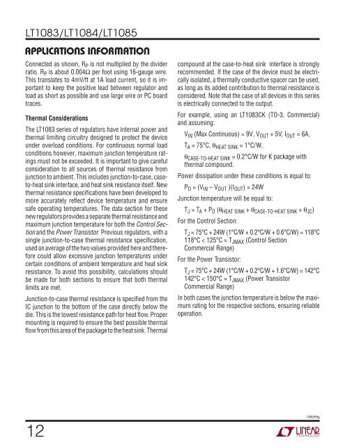
Connected as shown, RP is not multiplied by the divider<br />
ratio. RP is about 0.004Ω per foot using 16-gauge wire.<br />
This translates to 4mV/ft at 1A load current, so it is important<br />
to keep the positive lead between regulator and<br />
load as short as possible and use large wire or PC board<br />
traces.<br />
Thermal Considerations<br />
The <strong>LT1083</strong> series of regulators have internal power and<br />
thermal limiting circuitry designed to protect the device<br />
under overload conditions. For continuous normal load<br />
conditions however, maximum junction temperature ratings<br />
must not be exceeded. It is important to give careful<br />
consideration to all sources of thermal resistance from<br />
junction to ambient. This includes junction-to-case, caseto-heat<br />
sink interface, and heat sink resistance itself. New<br />
thermal resistance specifi cations have been developed to<br />
more accurately refl ect device temperature and ensure<br />
safe operating temperatures. The data section for these<br />
new regulators provides a separate thermal resistance and<br />
maximum junction temperature for both the Control Section<br />
and the Power Transistor. Previous regulators, with a<br />
single junction-to-case thermal resistance specifi cation,<br />
used an average of the two values provided here and therefore<br />
could allow excessive junction temperatures under<br />
certain conditions of ambient temperature and heat sink<br />
resistance. To avoid this possibility, calculations should<br />
be made for both sections to ensure that both thermal<br />
limits are met.<br />
Junction-to-case thermal resistance is specifi ed from the<br />
IC junction to the bottom of the case directly below the<br />
die. This is the lowest resistance path for heat fl ow. Proper<br />
mounting is required to ensure the best possible thermal<br />
fl ow from this area of the package to the heat sink. Thermal<br />
12<br />
compound at the case-to-heat sink interface is strongly<br />
recommended. If the case of the device must be electrically<br />
isolated, a thermally conductive spacer can be used,<br />
as long as its added contribution to thermal resistance is<br />
considered. Note that the case of all devices in this series<br />
is electrically connected to the output.<br />
For example, using an <strong>LT1083</strong>CK (TO-3, Commercial)<br />
and assuming:<br />
VIN (Max Continuous) = 9V, VOUT = 5V, IOUT = 6A,<br />
TA = 75°C, θHEAT SINK = 1°C/W,<br />
θCASE-TO-HEAT SINK = 0.2°C/W for K package with<br />
thermal compound.<br />
Power dissipation under these conditions is equal to:<br />
PD = (VIN – VOUT )(IOUT) = 24W<br />
Junction temperature will be equal to:<br />
TJ = TA + PD (θHEAT SINK + θCASE-TO-HEAT SINK + θJC) For the Control Section:<br />
TJ = 75°C + 24W (1°C/W + 0.2°C/W + 0.6°C/W) = 118°C<br />
118°C < 125°C = TJMAX (Control Section<br />
Commercial Range)<br />
For the Power Transistor:<br />
TJ = 75°C + 24W (1°C/W + 0.2°C/W + 1.6°C/W) = 142°C<br />
142°C < 150°C = TJMAX (Power Transistor<br />
Commercial Range)<br />
In both cases the junction temperature is below the maximum<br />
rating for the respective sections, ensuring reliable<br />
operation.<br />
108345fg


