LT1083/LT1084/LT1085 - Linear Technology
LT1083/LT1084/LT1085 - Linear Technology
LT1083/LT1084/LT1085 - Linear Technology

You also want an ePaper? Increase the reach of your titles
YUMPU automatically turns print PDFs into web optimized ePapers that Google loves.
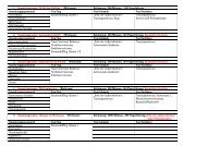
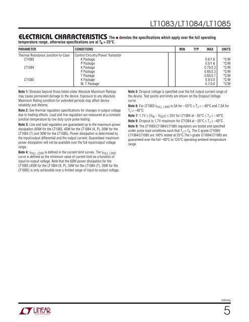
ELECTRICAL CHARACTERISTICS<br />
Note 1: Stresses beyond those listed under Absolute Maximum Ratings<br />
may cause permanent damage to the device. Exposure to any Absolute<br />
Maximum Rating condition for extended periods may affect device<br />
reliability and lifetime.<br />
Note 2: See thermal regulation specifi cations for changes in output voltage<br />
due to heating effects. Load and line regulation are measured at a constant<br />
junction temperature by low duty cycle pulse testing.<br />
Note 3: Line and load regulation are guaranteed up to the maximum power<br />
dissipation (60W for the <strong>LT1083</strong>, 45W for the <strong>LT1084</strong> (K, P), 30W for the<br />
<strong>LT1084</strong> (T) and 30W for the <strong>LT1085</strong>). Power dissipation is determined by<br />
the input/output differential and the output current. Guaranteed maximum<br />
power dissipation will not be available over the full input/output voltage<br />
range.<br />
Note 4: I FULL_LOAD is defi ned in the current limit curves. The I FULL_LOAD<br />
curve is defi ned as the minimum value of current limit as a function of<br />
input-to-output voltage. Note that the 60W power dissipation for the<br />
<strong>LT1083</strong> (45W for the <strong>LT1084</strong> (K, P), 30W for the <strong>LT1084</strong> (T), 30W for the<br />
<strong>LT1085</strong>) is only achievable over a limited range of input-to-output voltage.<br />
<strong>LT1083</strong>/<strong>LT1084</strong>/<strong>LT1085</strong><br />
The l denotes the specifi cations which apply over the full operating<br />
temperature range, otherwise specifi cations are at TA = 25°C.<br />
PARAMETER CONDITIONS MIN TYP MAX UNITS<br />
Thermal Resistance Junction-to-Case<br />
<strong>LT1083</strong><br />
<strong>LT1084</strong><br />
<strong>LT1085</strong><br />
Control Circuitry/Power Transistor<br />
K Package<br />
P Package<br />
K Package<br />
P Package<br />
T Package<br />
K Package<br />
M, T Package<br />
0.6/1.6<br />
0.5/1.6<br />
0.75/2.3<br />
0.65/2.3<br />
0.65/2.7<br />
0.9/3.0<br />
0.7/3.0<br />
°C/W<br />
°C/W<br />
°C/W<br />
°C/W<br />
°C/W<br />
°C/W<br />
°C/W<br />
Note 5: Dropout voltage is specifi ed over the full output current range of<br />
the device. Test points and limits are shown on the Dropout Voltage<br />
curve.<br />
Note 6: For <strong>LT1083</strong> I FULL_LOAD is 5A for –55°C ≤ TJ < – 40°C and 7.5A for<br />
T J ≥ –40°C.<br />
Note 7: 1.7V ≤ (V IN – V OUT) ≤ 25V for <strong>LT1084</strong> at –55°C ≤ T J ≤ – 40°C.<br />
Note 8: Dropout is 1.7V maximum for <strong>LT1084</strong> at –55°C ≤ T J ≤ –40°C.<br />
Note 9: The <strong>LT1083</strong>/<strong>LT1084</strong>/<strong>LT1085</strong> regulators are tested and specifi ed<br />
under pulse load conditions such that T J ≅ T A. The C-grade <strong>LT1083</strong>/<br />
<strong>LT1084</strong>/<strong>LT1085</strong> are 100% tested at 25°C.The I-grade <strong>LT1084</strong>/<strong>LT1085</strong> are<br />
guaranteed over the full –40°C to 125°C operating ambient temperature<br />
range.<br />
108345fg<br />
5