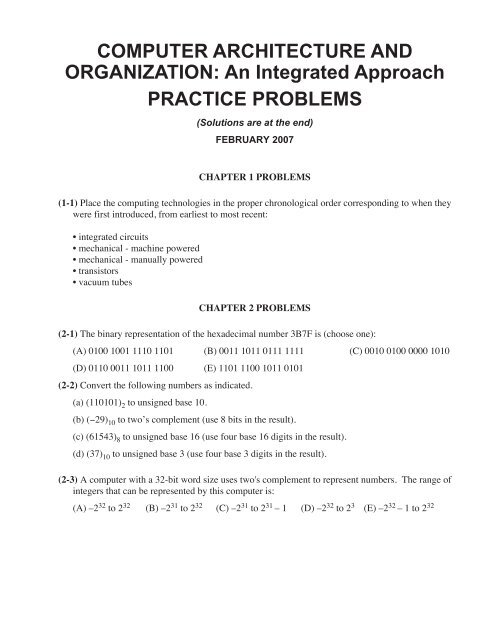
COMPUTER ARCHITECTURE AND ORGANIZATION: An ... - IIUSA
COMPUTER ARCHITECTURE AND ORGANIZATION: An ... - IIUSA
COMPUTER ARCHITECTURE AND ORGANIZATION: An ... - IIUSA

Create successful ePaper yourself
Turn your PDF publications into a flip-book with our unique Google optimized e-Paper software.
<strong>COMPUTER</strong> <strong>ARCHITECTURE</strong> <strong>AND</strong><br />
<strong>ORGANIZATION</strong>: <strong>An</strong> Integrated Approach<br />
PRACTICE PROBLEMS<br />
(Solutions are at the end)<br />
FEBRUARY 2007<br />
CHAPTER 1 PROBLEMS<br />
(1-1) Place the computing technologies in the proper chronological order corresponding to when they<br />
were first introduced, from earliest to most recent:<br />
• integrated circuits<br />
• mechanical - machine powered<br />
• mechanical - manually powered<br />
• transistors<br />
• vacuum tubes<br />
CHAPTER 2 PROBLEMS<br />
(2-1) The binary representation of the hexadecimal number 3B7F is (choose one):<br />
(A) 0100 1001 1110 1101 (B) 0011 1011 0111 1111 (C) 0010 0100 0000 1010<br />
(D) 0110 0011 1011 1100 (E) 1101 1100 1011 0101<br />
(2-2) Convert the following numbers as indicated.<br />
(a) (110101) 2 to unsigned base 10.<br />
(b) (−29) 10 to two’s complement (use 8 bits in the result).<br />
(c) (61543) 8 to unsigned base 16 (use four base 16 digits in the result).<br />
(d) (37) 10 to unsigned base 3 (use four base 3 digits in the result).<br />
(2-3) A computer with a 32-bit word size uses two's complement to represent numbers. The range of<br />
integers that can be represented by this computer is:<br />
(A) –2 32 to 2 32 (B) –2 31 to 2 32 (C) –2 31 to 2 31 – 1 (D) –2 32 to 2 3 (E) –2 32 – 1 to 2 32
(2-4) Computer A uses the following 32-bit floating-point representation of real numbers:<br />
S<br />
Mantissa Exponent<br />
31 30 7 6 0<br />
Computer B uses the following floating point representation scheme:<br />
S<br />
Mantissa Exponent<br />
31 30 8 7 0<br />
Which of the following statements is true with regard to Computer B’s method of representing<br />
floating-point numbers over Computer A’s method?<br />
(A) both the range and precision are increased<br />
(B) the range is increased but the precision is decreased<br />
(C) the range is decreased but the precision is increased<br />
(D) both the range and precision are decreased<br />
(E) both the range and precision remain the same<br />
(2-5) (ref: Stallings, 1999) A normalized floating point representation has an exponent e with a<br />
representation that lies in the range 0 ≤ e ≤ X, in excess q, with a base b and a p digit fraction. Note<br />
the emphasis on representation, as opposed to value.<br />
(a) What are the largest and smallest positive values that can be represented?<br />
(b) What are the largest and smallest gaps?<br />
(c) What is the number of representable numbers?<br />
(2-6) Express -1/32 in the IEEE 754 single precision format.<br />
(2-7) For parts (a) through (d), use a floating point representation with a sign bit in the leftmost<br />
position, followed by a three-bit excess 4 exponent, followed by a normalized six-bit fraction in<br />
base 4. Zero is represented by the bit pattern 0 000 000000.<br />
(a) What decimal number is represented by the bit pattern: 1 100 010000?<br />
(b) Show the bit pattern for the smallest non-zero positive representable number.<br />
(c) Show the bit pattern for the largest positive representable number.<br />
(d) There are a total of 10 bits in this floating point representation, so there are 2 10 = 1024 unique<br />
bit patterns. How many of these bit patterns are valid? (Remember: 0 = 0 000 000000).<br />
(2-8) Represent (107.875) 10 in the IEEE-754 single precision floating point representation which has a<br />
sign bit, an eight-bit excess 127 exponent, and a normalized 23-bit significand in base 2 with a<br />
hidden 1 to the left of the radix point. Truncate the fraction if necessary by chopping bits as<br />
necessary. Show your work.
CHAPTER 3 PROBLEMS<br />
(3-1) Show the results of adding/subtracting the following pairs of six-bit (i.e. one sign bit and five<br />
data bits) two’s complement numbers and indicate whether or not overflow/underflow occurs for<br />
each case:<br />
0 1 0 1 1 0 1 0 1 0 1 1 1 1 1 1 1 1<br />
+ 0 0 1 0 0 1 + 1 0 0 1 0 1 + 0 0 0 1 1 1<br />
------------- ------------- -------------<br />
0 1 0 1 1 0 1 1 1 1 1 0 1 0 0 0 0 1<br />
- 0 1 1 1 1 1 - 1 0 0 1 0 1 - 0 1 1 1 0 1<br />
------------- ------------- -------------<br />
(3-2) (From Hamacher et al, 1990) Perform A×B and A/B on unsigned A=10101 and B=00101<br />
manually. (Just use pen and paper; do not show the serial multiplication or division menthods.)<br />
(3-3) Show how the unsigned serial multiplication method would compute M × Q where M = 10110<br />
and Q = 01101. M and Q are unsigned numbers. For each step, describe in words what is<br />
happening (shift left, shift right, add/subtract M or Q into product, set a bit, etc.), and show the<br />
product (or partial product) for that step. (Note: Q is the multiplier and M is the multiplicand.)<br />
Step # Product Action<br />
0 C=0 M=10110 Q=01101 Initial values _<br />
C A Q _<br />
(3-4) Use the Booth algorithm (not bit pair recoding) to multiply 0110 by 0110.<br />
(3-5) Use the modified Booth algorithm (that is, use bit pair recoding) to multiply signed numbers<br />
010101 (multiplicand) by 110110 (multiplier).<br />
(3-6) Use the Booth and bit-pair recoding techniques to multiply (-10 × -10 = 100) 10 .<br />
(3-7) Boolean expressions are shown below for the difference diffi = (xi – yi ) and borrow bi+1 outputs<br />
of a full subtractor. The subscripts denote the relative position of a full subtractor in a ripple-borrow<br />
subtractor:<br />
diffi = xiyibi + xiyibi + xiyibi + xiyibi bi+1 = xibi + xiyi + yibi We can factor the second equation and obtain:<br />
bi+1 = xiyi + bi (xi + yi )<br />
which can be rewritten as:<br />
bi+1 = Gi + Pib i<br />
where: Gi = xiyi and Pi = xi + yi .<br />
The G i and P i terms are referred to as generate and propagate functions, respectively, for the effect<br />
they have on the borrow. When G i = 1, a borrow is generated at stage i. When P i = 1, then a borrow is<br />
propagated through stage i if either x i is 0 or y i is 1. Create Boolean equations for b 0 , b 1 , b 2 , and b 3 for<br />
a borrow-lookahead subtractor in terms of P i and G i . Hint: Assume b 0 = 0.
CHAPTER 4 PROBLEMS<br />
(4-1) Which of the following operations does function baz in the ARC program shown below carry<br />
out? The parameters A and B are passed to the function and returned from it are passed via the<br />
stack. B is closer to the stack pointer than A. Circle one of these operations:<br />
(A) min (A , B) (B) max(A , B) (C) addcc(A , B) (D) subcc(A , B)<br />
(E) (A == B)
(a) How large can the stack grow, in bytes? (Leave your answer as an equation in powers of<br />
two, e.g. 8 + 2 10 .)<br />
(b) When a joystick is moved, the horizontal (joy_x) and vertical (joy_y) positions of the<br />
joystick are updated in memory locations (FFFFF0)16 and (FFFFF4)16, respectively. When the<br />
number ‘1’ is written to memory location (FFFFEC) 16 the screen flashes, and then location<br />
(FFFFEC)16 is automatically cleared to zero by the hardware (the software does not have to clear<br />
it). Write an ARC program that flashes the screen every time the joystick moves. Use the skeleton<br />
program shown below. The ARC instruction set is summarized at the end of the exam.<br />
.begin<br />
ld [joy_x], %r7 ! %r7 and %r8 now point to the<br />
ld [joy_y], %r8 ! joystick x and y locations<br />
ld [flash], %r9 ! %r9 points to the flash location<br />
loop: ld %r7, %r1 ! Load current joystick position<br />
ld %r8, %r2 ! in %r1=x and %r2=y<br />
ld [old_x], %r3 ! Load old joystick position<br />
ld [old_y], %r4 ! in %r3=x and %r4=y<br />
orncc %r3, %r0, %r3 ! Form one’s complement of old_x<br />
addcc %r3, 1, %r3 ! Form two’s complement of old_x<br />
addcc %r1, %r3, %r3 ! %r3
(4-4) The instruction set shown below should be new to you. The ZERO instruction has been removed<br />
in this version although its description is left in place so that you can understand its function. How can<br />
the remaining instructions be used to implement the ZERO function on register 5? No memory storage<br />
is to be used. Show the 16-bit object code instruction(s).<br />
MNEMONIC OPCODE<br />
OPER<strong>AND</strong> FIELDS<br />
Operand A Operand B Result<br />
DESCRIPTION<br />
ZERO 0000000 –– –– X Set contents of Result register to zero.<br />
COPY<br />
ADD<br />
SUB<br />
MULTIPLY<br />
COMP<br />
INC<br />
DEC<br />
HALT<br />
LOAD<br />
0000001 X –– X Copy Operand A register to Result<br />
register.<br />
0000010 X X X<br />
0000011 X X X<br />
0000100 X X X<br />
0000101 X –– X<br />
0000110 X –– X<br />
0000111 X –– X<br />
0001000 –– –– –– Halt the processor.<br />
Add Operand A and Operand B<br />
registers, placing result in Result<br />
register.<br />
Subtract Operand B register from<br />
Operand A register, placing result in<br />
Result register.<br />
Multiply the Operand A and Operand<br />
B registers, placing the result in Result<br />
register.<br />
Copy the complement of the Operand<br />
A register into the Result register.<br />
Increment Operand A register by 1,<br />
placing result in Result register.<br />
Decrement Operand A register by 1,<br />
placing result in Result register.<br />
10 Destination –– Address Load Destination register with contents<br />
of memory at location Address.<br />
STORE 11 Source –– Address Store Source register in memory at<br />
location Address.<br />
NOTE: There are 8 registers in this architecture.<br />
Source Source<br />
Opcode Operand A Operand B Result<br />
7 bits 3 bits 3 bits 3 bits
CHAPTER 5 PROBLEMS<br />
(5-1) List the microinstructions that are executed in interpreting the ARC "st %r1, %r2, %r3"<br />
instruction. Start with microinstruction 0. Just list the microinstruction numbers, not the code.<br />
(5-2) Write the binary form for the microinstructions shown below. Use the value 0 for any fields that<br />
are not needed.<br />
1615: R[temp1] ← R[rs1]; GOTO 21;<br />
21: R[temp2] ← NOR(R[temp0], R[temp0]);<br />
60:<br />
61:<br />
A<br />
B<br />
C<br />
M<br />
M<br />
M<br />
U<br />
U<br />
U RW<br />
A X B X C X D R ALU COND JUMP ADDR<br />
(5-3) Microcode: <strong>An</strong> ALU that operates on 8-bit operands can be implemented with a read-only<br />
memory (ROM) that behaves as a lookup table (LUT), in which the data and control bits are treated<br />
alike. The block diagram shown below illustrates the external behavior of the ALU that we would like<br />
to implement with a ROM LUT. The A and B lines are for the operand inputs, and the F lines (that is,<br />
the control inputs) select the ALU function according to the truth table shown below. The Cin and Cout lines are for the carry in and the carry out, respectively. The carry out is always 0 when an addition is<br />
not taking place. The 8-bit output appears on the Z lines. Assume that a two’s complement<br />
representation is used. Fill in the missing entries in the truth table below.<br />
[HINT: The solution for the first row is all 1's for Z7 - Z0.] F 1 F 0 Function<br />
0<br />
0<br />
1<br />
1<br />
0<br />
1<br />
0<br />
1<br />
NOR<br />
Multiply<br />
<strong>AND</strong><br />
Add<br />
Address lines<br />
A 7<br />
.<br />
.<br />
A0 B7 .<br />
.<br />
B0 Cin F 1<br />
F 0<br />
8<br />
8<br />
1<br />
2<br />
ROM<br />
LUT<br />
A 7 F 0 Z 7 Z 6 Z 5 Z 4 Z 3 Z 2 Z 1 Z 0 C out<br />
A6 A5 A4 A3 A2 A1 A0 B7 B6 B5 B4 B3 B2 B1 B0 Cin F1 0 0 0 0 0 0 0 0 0 0 0 0 0 0 0 0 0 0 0 _ _ _ _ _ _ _ _ 0<br />
_ _ _ _ _ _ _ _ 0 0 0 0 0 0 1 1 0 0 1 0 0 0 1 0 1 0 1 0<br />
1 1 1 1 1 1 1 1 1 1 1 1 1 1 1 1 1 1 1 _ _ _ _ _ _ _ _ _<br />
8<br />
1<br />
Z 7<br />
.<br />
.<br />
Z 0<br />
C out<br />
Data out lines
CHAPTER 6 PROBLEMS<br />
(6-1) Translate the following Pascal code into SPARC (note: this is a variation of a problem from the<br />
Tanenbaum Structured Computer Organization textbook).<br />
/* Compute min of i and j */<br />
function min (i, j: Int): Int /* i and j are parameters, min returns Int*/<br />
var m: Int;<br />
begin<br />
if i < j then m := i else m := j;<br />
min := m /* This is how a Pascal function returns a value */<br />
end;<br />
(6-2) Translate the single line indicated in the following ARC code into object code. Remember:<br />
branch displacements are in terms of 4-byte words, not bytes. (That is, an offset of 8 bytes is<br />
represented as 2, because it is equivalent to an offset of 2 words.)<br />
.begin<br />
.org 0<br />
srl %r2, 10, %r2 ans: 10 00010 100110 00010 1 0000000001010<br />
(6-3) Disassemble the following ARC object code into a source statement. Since there is not enough<br />
information in the object code to determine symbol names, use numbers (offsets, like +5 or −12)<br />
instead, if needed.<br />
00000010 10000000 00000000 00000011<br />
(6-4) Given the assembly language program shown on the next page, which uses an assembly<br />
language syntax that should be new to you, construct a symbol table. As with the ARC assembly<br />
language, each instruction in this assembly language occupies four bytes. Not all of the lines in the<br />
table will be needed. Do not try to figure out what the program does – it is not helpful to know this.<br />
Mark any undefined symbols with an “X.” All values are given in base 10. Registers are named R0,<br />
R1, and R3
All numbers are given in base 10<br />
K EQU 77<br />
P EQU 1<br />
ORG 32<br />
JUMP MAIN<br />
PMUL: SUB 2,R0<br />
LOAD A,R1<br />
BZERO ANOTZ<br />
LOAD 0,R1<br />
JUMP DONE<br />
ANOTZ: LOAD B,R3<br />
.<br />
BZERO<br />
LOAD<br />
BNOTZ<br />
0,R3<br />
JUMP DONE<br />
BNOTZ: LOAD 0,R1<br />
STORE R1,A<br />
BZERO PMUL<br />
DONE: JUMP DONE<br />
A: 12<br />
B: 15<br />
Symbol Value<br />
K 77<br />
P 1<br />
MAIN X<br />
PMUL 36<br />
A 88<br />
ANOTZ 56<br />
DONE 84<br />
B 92<br />
BNOTZ 72<br />
(6-5) Define a SPARC macro mov that copies its first argument (a literal) into its second argument (a<br />
register). For example, the code<br />
copies 10 into register %r24.<br />
mov 10, %r24<br />
(6-6) In the compiled SPARC code used in the book, both call and jmpl need two instruction cycles<br />
to complete. Both instructions are followed by a nop if there is no nearby instruction that can replace<br />
the nop. The ret instruction is actually a pseudo-instruction that translates to:<br />
jmpl %r15+8, %r0<br />
In the other code examples, however, the following code is used for returning from a subroutine call:<br />
jmpl %r15+4, %r0<br />
What would happen if we used the %r15+4 version for the ret in the compiled code? In what way(s)<br />
would the program behave differently?<br />
ans: The program would still work correctly, but the return would go to the nop instruction that<br />
follows the call, thus wasting an instruction cycle.
(6-7) Given an architecture that implements the following instructions:<br />
Mnemonic Operand(s) Meaning<br />
PUSH arg Push contents of memory location arg onto stack<br />
POP arg Pop stack into memory location arg<br />
BA label Branch to label<br />
ADD arg1, arg2, arg3 arg3
CHAPTER 7 PROBLEMS<br />
(7-1) A cache has a 95% hit ratio, an access time of 100ns on a cache hit, and an access time of 800ns<br />
on a cache miss. Compute the effective access time.<br />
(7-2) (From Stallings, 1999) A set associative cache consists of 64 slots divided into 4-slot sets. Main<br />
memory contains 4K blocks of 128 words each. Show the format of the main memory address.<br />
(7-3) Using the page table shown below, translate virtual address 2050 into a physical address, and<br />
translate physical address 25 into a virtual address. Address length is 16 bits, page size is 2048 words.<br />
Physical memory has 4 page frames.<br />
Page Present (1-in/0-out) Page Frame<br />
0 1 3<br />
1 1 2<br />
2 1 0<br />
3 0 --<br />
...<br />
(7-4) A computer has 16 pages of virtual address space but only 4 page frames. Initially the memory<br />
is empty. A program references the virtual pages in the order: 0 2 4 5 2 4 3 11 2 10.<br />
(a) Which references cause a page fault with the LRU page replacement policy?<br />
(b) Which references cause a page fault with the FIFO page replacement policy?<br />
(7-5) When running a particular program with N memory accesses, a computer with a cache and<br />
paged virtual memory generates a total of M cache misses and F page faults. T1 is the time for a<br />
cache hit; T2 is the time for a main memory hit; and T3 is the time to load a page into main memory<br />
from the disk.<br />
(a) What is the cache hit ratio?<br />
(b) What is the main memory hit ratio? That is, what percentage of main memory accesses do not<br />
generate a page fault?<br />
(c) What is the overall effective access time for the system?<br />
(7-6) Four 256-word × 8-bit PROM chips are used to produce a total capacity of 1024-word × 8-bits.<br />
How many address bus lines are required? (Circle one.)<br />
(A) 4 (B) 8 (C) 10 (D) 16 (E) 32<br />
(7-7) A direct mapped cache consists of 4 blocks of 16 words per block. Main memory contains 32K<br />
blocks of 16 words each. The hit time for a cache access is 10 ns, and the miss time is 200 ns,<br />
which includes the time to transfer the missed block from the main memory to the cache. Note:<br />
When referring to memory, 1K = 1024. Compute the hit ratio for a program that loops 10 times<br />
from locations 0 – 64.<br />
(7-8) A set associative cache consists of 64 slots divided into 4-slot sets. Main memory contains 4K<br />
blocks of 128 bytes each. Show the format of the main memory address. (Tag, Slot or Set, and Byte<br />
fields.)
(7-9) <strong>An</strong> operating system uses a Least Recently Used (LRU) page replacement algorithm. Consider<br />
the following page reference ordering (pages are referenced from left to right):<br />
1, 8, 1, 7, 8, 2, 7, 2, 1, 8, 3<br />
Which of the following is the number of page faults that are generated for this particular LRU case<br />
assuming that the process has been allocated four page frames, and that initially, none of the pages<br />
are in the main memory? (Circle one.)<br />
(A) 6 (B) 5 (C) 4 (D) 3 (E) 7<br />
(7-10) True or False (choose one): The purpose of virtual memory is to increase the speed of main<br />
memory, and the purpose of cache memory is to increase the size of main memory.<br />
(7-11) A direct mapped cache consists of 256 slots. Main memory contains 32K blocks of 16 words<br />
each. Access time of the cache is 10 ns, and the time required to fill a cache slot is 200 ns. Loadthrough<br />
is not used; that is, when an accessed word is not found in the cache, the entire block is<br />
brought into the cache, and the word is then accessed through the cache. Initially, the cache is empty.<br />
Note: When referring to memory, 1K = 1024.<br />
(a) Show the format of the memory address (show the number of bits in the Tag, Block or Set (as<br />
appropriate), and Byte fields, and their relative position from left to right.)<br />
(b) Compute the hit ratio and effective access time for a program that loops 10 times from locations 15<br />
– 52 (there is no need to divide it out, without a calculator). Note that although the memory is accessed<br />
twice during a miss (once for the miss, and once again to satisfy the reference), a hit does not occur for<br />
this case. To a running program, only a single memory reference is observed.<br />
Hit ratio =<br />
Eff. access time =<br />
No. times referenced words are in cache<br />
Total number of memory accesses<br />
(No. hits) (Time per hit) + (No. misses) (Time per miss)<br />
Total number of memory accesses<br />
(7-12) A virtual memory system has a page size of 512 bytes, eight virtual pages, and four physical<br />
page frames. The page table is as follows:
Present bit Page frame field<br />
Page # Disk address<br />
0<br />
1<br />
2<br />
3<br />
4<br />
5<br />
6<br />
7<br />
0<br />
0<br />
1<br />
0<br />
1<br />
0<br />
1<br />
0<br />
01001011100<br />
11101110010<br />
10110010111<br />
00001001111<br />
01011100101<br />
10100111001<br />
00110101100<br />
01010001011<br />
(a) What is the main memory address for virtual address 1024?<br />
(b) What is the virtual address for main memory address 512?<br />
(7-13) A memory has 2 24 addressable locations. What is the smallest width in bits that the address can<br />
be while still being able to address all 2 24 locations?<br />
(7-14) If a virtual memory system has 4 pages in real memory and the rest must be swapped to disk,<br />
determine the hit ratio for the following page address system. Assume memory starts empty. Use<br />
the First In First Out (FIFO) page replacement policy. Choose the closest answer.<br />
(A) 10% (D) 31%<br />
(B) 15% (E) 50%<br />
(C) 25%<br />
PAGE REQUESTS: 2 5 3 4 1 4 7 2 1 3 1 7 4 5 4 6<br />
(7-15) A memory system has a two-level cache in which Level 1 is closer to the CPU than Level 2. The<br />
hit time for the Level 1 cache is T1 and the hit time for the Level 2 cache is T2. The miss time for<br />
the Level 2 cache is T3. On a cache miss at either level, the miss time includes the time to read in a<br />
block and deliver the requested word. What is the effective access time of the memory system if<br />
the hit ratios of both caches are 90%? <strong>An</strong> equation for the effective access time of a two-level<br />
cache is shown below:<br />
T EFF =<br />
xx<br />
xx<br />
00<br />
xx<br />
01<br />
xx<br />
11<br />
xx<br />
(No. on±chip cache hits) (Time per on±chip cache hit) +<br />
(No. off±chip cache hits) (Time per off±chip cache hit) +<br />
(No. off±chip cache misses) (Time per off±chip cache miss)<br />
Total number of memory accesses<br />
CHAPTER 8 PROBLEMS<br />
(8-1) A hard magnetic disk with a single platter rotates once every 16 ms. There are 8 sectors on<br />
each of 1000 tracks. <strong>An</strong> interleave factor of 1:2 is used. What is the fastest possible time to copy a<br />
track from the top side of the platter to the corresponding track on the bottom side of the platter?<br />
Assume that the sectors must be read in numerical order starting from 0, that the top and bottom
tracks must be mirror images, that any number of sectors can be read from the top track before<br />
writing them to the bottom track, and that simultaneous reading and writing is not allowed (even on<br />
different tracks.)<br />
(8-2) Consider a disk drive with the following characteristics:<br />
7200 revolutions per minute rotation speed<br />
7 msec average seek time<br />
256 sectors per track, with 512 bytes per sector<br />
2048 tracks per surface<br />
16 surfaces<br />
1 head per surface, all heads move together as a group<br />
reading and writing cannot be done at the same time<br />
(a) What is the total capacity of the disk drive?<br />
(b) What is the data transfer rate in bytes per second for this drive? That is, once the head is<br />
positioned over the sector to be read, what is the data transfer rate?<br />
(c) What is the average time to transfer a whole sector from one track to another track?<br />
(8-3) A number of disks, a CPU, and the main memory are all connected to the same 10 MHz 32-bit<br />
bus. The disk has a transfer rate of 2 MBytes/sec. The CPU and main memory can both keep pace<br />
with the bus. How many disks can be simultaneously transmitting?<br />
CHAPTER 9 PROBLEMS<br />
(9-1) Construct an SEC code for EBCDIC ‘T’. When constructing the code, number the bits from<br />
right to left starting with 1 (the same way it is done in the book).<br />
(9-2) Construct the SEC code for the Unicode character ‘1/4’ = 00BC 16 using even parity. Hint: check<br />
bits go in positions that correspond to powers of 2.<br />
(9-3) If 7-digit telephone numbers are assigned so that misdialing one digit results in an unassigned<br />
number, how many numbers can be assigned?<br />
(9-4) For SEC of 7-digit phone numbers, we need to add check digits such that the Hamming<br />
distance(H.D.) is 3 (for error correction of p digits, we need H.D. = 2p+1. For SEC, p=1 so H.D. is 3).<br />
How many check digits should we add?<br />
(9-5) In alphabetic encryption (AE), a string of characters is mapped into a different, longer string of<br />
characters consisting of only upper case letters. The AE code is shown below:<br />
Letter Code Letter Code Letter Code<br />
A 00000 J 01001 S 10010<br />
B 00001 K 01010 T 10011<br />
C 00010 L 01011 U 10100<br />
D 00011 M 01100 V 10101<br />
E 00100 N 01101 W 10110<br />
F 00101 O 01110 X 10111<br />
G 00110 P 01111 Y 11000<br />
H 00111 Q 10000 Z 11001<br />
I 01000 R 10001
(a) Compute the checksum word for the AE characters C, D, E, F and G. Use both longitudinal and<br />
vertical redundancy checking.<br />
(b) A receiver sees the following bit pattern, which is Hamming encoded using even parity (the<br />
way it is done in the book). What AE character was transmitted?<br />
(9-6) A single-user workstation is attached to a local network. The workstation accesses files over the<br />
network from a file server. The average access time is 0.09 seconds per page. A similar stand-alone<br />
workstation accesses files from its own local disk with an average access time of 0.03 seconds per<br />
page. A particular program accesses and processes a 300-page file. The time to process the file<br />
once the data is in memory is 45 seconds. What is the ratio of the total time to access and process<br />
the file for the local network workstation to the total time for the stand-alone workstation?<br />
(A) 3/1 (D) 5/2<br />
(B) 4/3 (E) 1/1<br />
(C) 8/5<br />
APPENDIX A PROBLEMS<br />
(A-1) The combinational circuit given below is implemented with two N<strong>AND</strong> gates. To which of the<br />
following individual gates is it equivalent?<br />
a<br />
b<br />
(A) NOT (B) OR (C) <strong>AND</strong> (D) XOR (E) NOR<br />
(A-2) Derive function x represented by the following circuit. The prime symbol (') has the same<br />
meaning as overbar.<br />
a<br />
b<br />
a<br />
b<br />
c<br />
(A) ab + a'bc' (B) (a + b)(a' + b + c') (C) ab + a'bc' (D) (ab)(a'bc') (E) bc'<br />
x
(A-3) Design a binary-to-Gray code converter using an 8-to-1 MUX, a 4-to-1MUX, and a 16-to-1<br />
MUX. Use the truth table shown below:<br />
x2 x1 x0 | z2 z1 z0<br />
---------+---------<br />
0 0 0 | 0 0 0<br />
0 0 1 | 0 0 1<br />
0 1 0 | 0 1 1<br />
0 1 1 | 0 1 0<br />
1 0 0 | 1 1 0<br />
1 0 1 | 1 1 1<br />
1 1 0 | 1 0 1<br />
1 1 1 | 1 0 0<br />
(A-4) Design a circuit that implements function p below using <strong>AND</strong>, OR, and NOT gates. DO NOT<br />
change the form of the equation. The circuit should implement this function exactly.<br />
f(i 0 , i 1 , i 2 ) = i 2 (i 0 i 1 + i 0 i 1 )<br />
(A-5) Label and connect the MUXes shown below to implement function F:<br />
0<br />
1<br />
F(A,B,C,D) = AB(CD + CD) + AB(CD) + AB(CD + CD)<br />
0<br />
1<br />
(A-6) The black box in the following figure consists of a combinational logic unit that uses only <strong>AND</strong>,<br />
OR, and NOT gates.<br />
x<br />
y<br />
z<br />
0<br />
1<br />
Black Box f(x, y, z)<br />
The function f(x, y, z) = 1 whenever x, y are different and 0 otherwise. Which of the following<br />
equations leads to the correct design for the combinational logic unit? The prime symbol (') in X'<br />
has the same meaning as an overbar.<br />
(A) x'y + xy' (B) x + y'z (C) x'y'z' + xy'z (D) xy + y'z + z' (E) x'z + xy + y'z'<br />
(A-7) How many distinct Boolean functions of 3 variables are there? This question is not asking how<br />
many possible unique combinations of 3 variables there can be, but rather, how many unique<br />
functions of those 3 variables can there be?<br />
00<br />
01<br />
10<br />
11<br />
F
(A) 16 (B) 64 (C) 256 (D) 512 (E) 1024<br />
(A-8) Create a state transition diagram that outputs a 1 whenever the sequence of two-bit inputs<br />
00→01 * →11 is detected. The asterisk means that the bit-pair 01 can appear any number of times<br />
at that position in the sequence, including not at all (zero times). Show the state transition diagram<br />
only (do not create a state table or draw a circuit).<br />
(A-9) Design a finite state machine (FSM) that has two control lines C0 and C1. The FSM has an<br />
output Z that is a 1 if C1C0=00, a 0 ifC1C0=01, the value of its current output if C1C0=10, and the<br />
complement of its current output ifC1C0=11. Just draw a state transition diagram that describes the<br />
behavior of the FSM.<br />
(A-10) For the FSM described by the state table shown below,<br />
(a) What is the smallest number of flip-flops needed to implement the FSM? (Do not apply any<br />
state reduction techniques.)<br />
(b) How many Boolean functions need to be created to implement this FSM? That is, how many<br />
next-state and output functions are there?<br />
(A-11) Design a sequential machine that outputs a 1 when the last three inputs are 011 or 110. Note<br />
that sequences can overlap, so that an input sequence of 0110 will produce an output sequence of<br />
0011. Just show the state transition diagram. Do not reduce the diagram or draw a circuit.<br />
(A-12) Given the state transition diagram shown below, design a circuit for this state machine using D<br />
flip-flop(s) and one 4-to-16 decoder with OR gates. For the state assignment, use the bit pattern<br />
that corresponds to the position of each letter in the alphabet, starting from 0 (A = 000, B = 001, C<br />
= 010, etc.).
0/0<br />
A<br />
input/outputs<br />
0/0<br />
1/0<br />
1/0<br />
C B<br />
1/0<br />
0/0<br />
1/1<br />
D E<br />
0/0 0/1<br />
1/0<br />
Present<br />
State<br />
A<br />
B<br />
C<br />
D<br />
E<br />
Input (x)<br />
0 1<br />
(A-13) Design an FSM using D flip-flops and the smallest possible ROM for a remote control that<br />
operates a TV:0, a VCR:1, and a CATV:2 device. The user selects a device by pressing the corresponding<br />
key. Once a device is selected, the user can increase the channel number (3) or decrease the<br />
channel number (4). The input (0, 1, 2, 3, or 4) is repeated on the corresponding output port (one for<br />
each device), except for 0, 1, and 2 which produce 0's at all outputs. (Hint: The STD is easier to draw<br />
if you use base 10.)<br />
(A-14) Consider the following circuit which contains a 3-bit register and a black box with some<br />
combinational logic:<br />
CLOCK<br />
D1<br />
Q1<br />
D2<br />
Q2<br />
D3<br />
Q3<br />
Black box of<br />
combinational logic<br />
The initial state of the circuit is Q 1 Q 2 Q 3 = 000. The circuit generates the sequence<br />
(010) → (110) → (001) → (001) → ... → (001)<br />
on successive clock cycles. Which of the following sets of equations are implemented by the<br />
combinational logic in the black box? The prime symbol (') in X' has the same meaning as an<br />
overbar.
(A) D 1 = Q 1 'Q 2 'Q 3 ' D 2 = Q 1 ' D 3 = Q 2<br />
(B) D 1 = Q 2 Q 3 ' D 2 = Q 1 Q 2 ' D 3 = Q 1 Q 2 Q 3 '<br />
(C) D 1 = Q 1 + Q 2 D 2 = Q 1 ' D 3 = Q 1 Q 2<br />
(D) D1 = Q1'Q2Q3' D2 = Q1'Q2'Q3' + Q1'Q2Q3' D3 = Q1Q2Q3' + Q1'Q2'Q3 (E) D1 = Q1Q2Q3' D2 = Q1'Q2'Q3' + Q1'Q2'Q3' D3 = Q1'Q2Q3' (A-15) Design a control unit for a simple hand-held video game in which a juggler on the display<br />
catches objects. Treat this as an FSM problem, in which you only show the state transition<br />
diagram. Do not show a state table, state assignment, or a circuit. The input to the control unit is<br />
a two-bit vector in which 00 means “Move Left,” 01 means “Move Right,” 10 means “Do Not<br />
Move,” and 11 means “Halt.” The two-bit output Z is 11 if the machine is currently halted, and is<br />
00, 01, or 10 otherwise, corresponding to the input patterns 00, 01, and 11. That is, the two-bit<br />
output is identical to the two-bit input, except when the machine is halted, in which case the<br />
output is 11 regardless of the input. Once the machine is halted, it must remain in the halted<br />
state indefinitely. Show only the state transition diagram.
(1-1)<br />
SOLUTIONS<br />
CHAPTER 1 SOLUTIONS<br />
(1) mechanical - manually operated<br />
(2) mechanical - machine powered<br />
(3) vacuum tubes<br />
(4) transistors<br />
(5) integrated circuits<br />
CHAPTER 2 SOLUTIONS<br />
(2-1) (B) 0011 1011 0111 1111<br />
(2-2)<br />
(a) 53 10<br />
(b) 11100011 2<br />
(c) 6363 16<br />
(d) 11013 (2-3) (C) –231 to 231 – 1<br />
(2-4) (B) the range is increased but the precision is decreased<br />
(2-5)<br />
(a) Smallest = .1 × b-q Largest = (1 - b-p ) × b (X - q)<br />
(b) Smallest gap = b-p × b-q Largest gap = b-p × b (X - q)<br />
(c) 2 × (X + 1) × (b - 1) × b p-1 + 1<br />
(2-6)<br />
1 0 1 1 1 1 0 1 0 . 0 0 0 0 0 0 0 0 0 0 0 0 0 0 0 0 0 0 0 0 0 0 0<br />
S Exponent Fraction<br />
1/32 = (.00001) 2 = 1.0 x 2 -5 . The 1 to the left of the radix point is dropped, which is why the fraction is<br />
all 0's. The exponent is in excess 127 (not 128), so -5+127 = 122 for the exponent.<br />
(2-7) (a) –.1 4 × 4 4-4 = –.25 10<br />
(b) 0 000 010000<br />
(c) 0 111 111111<br />
(d) 2 (sign bit) × 2 3 (exponent) × 3 (first digit) × 4 2 (remaining digits) + 1 (zero) = 769
(2-8)<br />
0 1 0 0 0 0 1 0 1 . 1 0 1 0 1 1 1 1 1 0 0 0 0 0 0 0 0 0 0 0 0 0 0<br />
(3-1)<br />
CHAPTER 3 SOLUTIONS<br />
0 1 0 1 1 0 1 0 1 0 1 1 1 1 1 1 1 1<br />
+ 0 0 1 0 0 1 + 1 0 0 1 0 1 + 0 0 0 1 1 1<br />
------------- ------------- -------------<br />
0 1 1 1 1 1 0 1 0 0 0 0 0 0 0 1 1 0<br />
No overflow Overflow No overflow<br />
0 1 0 1 1 0 1 1 1 1 1 0 1 0 0 0 0 1<br />
- 0 1 1 1 1 1 - 1 0 0 1 0 1 - 0 1 1 1 0 1<br />
------------- ------------- -------------<br />
1 1 0 1 1 1 0 1 1 0 0 0 0 0 0 1 0 0<br />
No underflow No underflow Underflow<br />
(3-2)<br />
1 0 1 0 1 21<br />
x 0 0 1 0 1 5<br />
-----------<br />
1 0 1 0 1<br />
0 0 0 0 0<br />
1 0 1 0 1<br />
0 0 0 0 0 0<br />
0 0 0 0 0 0<br />
-----------------<br />
0 0 1 1 0 1 0 0 1 105<br />
00100 R1<br />
+--------<br />
00101 | 10101<br />
00101<br />
-------<br />
00001<br />
(3-3)<br />
Step # Product Action<br />
0 C=0 M=10110 Q=01101 Initial values _<br />
C A Q _<br />
1 0 10110 01101 Add M to A _<br />
2 0 01011 00110 Shift _
(3-4)<br />
3 0 00101 10011 Shift (no add) _<br />
4 0 11011 10011 Add M to A _<br />
5 0 01101 11001 Shift _<br />
6 1 00011 11001 Add M to A _<br />
7 0 10001 11100 Shift _<br />
8 0 01000 11110 Shift _<br />
0 1 1 0 Multiplicand<br />
0 1 1 0 Multiplier<br />
x 1 0 1 0 Booth recoded multiplier<br />
-------------------<br />
1 1 1 1 0 1 0 0 -1 x 0 1 1 0<br />
+ 0 0 1 1 0 1 x 0 1 1 0<br />
-------------------<br />
0 0 1 0 0 1 0 0<br />
(3-5)<br />
0 1 0 1 0 0 (Multiplicand)<br />
1 1 0 1 1 0 (Multiplier)<br />
0-1 1 0-1 0 Booth recoded multiplier<br />
x -1 2 -2 Bit-Pair recoded multiplier<br />
-------------------------------<br />
1 1 1 1 1 1 0 1 0 1 1<br />
+ 0 0 0 0 1 0 1 0 1<br />
+ 1 1 1 0 1 0 1 1<br />
-------------------------------<br />
1 1 1 1 0 0 1 0 1 1 1<br />
(3-6)<br />
Booth:<br />
1 1 1 1 0 1 1 0 -10 (Multiplicand)<br />
1 1 1 1 0 1 1 0 -10 (Multiplier)<br />
x 0 0 0-1 1 0-1 0 Booth recoded multiplier<br />
-------------------------------<br />
0 0 0 0 0 0 0 0 0 0 0 1 0 1 0 0 -10 x -2<br />
+ 1 1 1 1 1 1 1 1 1 0 1 1 0 0 0 0 -10 x 8<br />
+ 0 0 0 0 0 0 0 0 1 0 1 0 0 0 0 0 -10 x -16<br />
-------------------------------<br />
0 0 0 0 0 0 0 0 0 1 1 0 0 1 0 0 = 100<br />
Bit-pair:<br />
1 1 1 1 0 1 1 0 -10 (Multiplicand)<br />
1 1 1 1 0 1 1 0 -10 (Multiplier)
0 0 0-1 1 0-1 0 Booth recoded multiplier<br />
x 0 -1 2 -2 Bit-Pair recoded multiplier<br />
-------------------------------<br />
0 0 0 0 0 0 0 0 0 0 0 1 0 1 0 0 -10 x -2<br />
+ 1 1 1 1 1 1 1 1 1 0 1 1 0 0 0 0 -10 x 8<br />
+ 0 0 0 0 0 0 0 0 1 0 1 0 0 0 0 0 -10 x -16<br />
-------------------------------<br />
0 0 0 0 0 0 0 0 0 1 1 0 0 1 0 0 = 100<br />
(3-7)<br />
b 0 = 0<br />
b 1 = G 0 + P 0 b 0 = G 0<br />
b 2 = G 1 + P 1 b 1 = G 1 + P 1 G 0<br />
b 3 = G 2 + P 2 b 2 = G 2 + P 2 G 1 + P 2 P 1 G 0<br />
b 4 = G 3 + P 3 b 3 = G 3 + P 3 G 2 + P 3 P 2 G 1 + P 3 P 2 P 1 G 0<br />
(4-1) (B) max(A , B)<br />
(4-2)<br />
(a) 2 23 - 2 19 + 4<br />
(b)<br />
.begin<br />
CHAPTER 4 SOLUTIONS<br />
ld [joy_x], %r7 ! %r7 and %r8 now point to the<br />
ld [joy_y], %r8 ! joystick x and y locations<br />
ld [flash], %r9 ! %r9 points to the flash location<br />
loop: ld %r7, %r1 ! Load current joystick position<br />
ld %r8, %r2 ! in %r1=x and %r2=y<br />
ld [old_x], %r3 ! Load old joystick position<br />
ld [old_y], %r4 ! in %r3=x and %r4=y<br />
orncc %r3, %r0, %r3 ! Form one’s complement of old_x<br />
addcc %r3, 1, %r3 ! Form two’s complement of old_x<br />
addcc %r1, %r3, %r3 ! %r3
moved:<br />
addcc %r0, 1, %r5<br />
st %r5, %r9<br />
st %r1, [old_x]<br />
st %r2, [old_y]<br />
ba loop<br />
flash: #FFFFEC ! Location of flash register<br />
joy_x: #FFFFF0 ! Location of joystick x register<br />
joy_y: #FFFFF4 ! Location of joystick y register<br />
old_x: 0 ! Previous x position<br />
old_y: 0 ! Previous y position<br />
.end<br />
(4-3)<br />
(4-4)<br />
There is more than one solution. Here is one:<br />
0000011 001 001 101<br />
CHAPTER 5 SOLUTIONS<br />
(5-1) Note that %r1 goes in the rd field for an st instruction:<br />
11 00001 000100 00010 0 00000000 00011<br />
op rd op3 rs1 i rs2<br />
DECODE: 1 11 000100 00 = 1808<br />
Microinstructions: 0, 1, 1808, 1809, 40, 41, 42, 43, 44, 2047
(5-2)<br />
1615: 000000 1 000000 0 100010 0 0 0 0001 110 00000010101<br />
21: 100001 0 100001 0 100011 0 0 0 0010 000 00000000000<br />
(5-3)<br />
00000000 00000000 0 00 00000000 0<br />
00000111 00000011 0 01 00010101 0<br />
11111111 11111111 1 11 11111110 1<br />
CHAPTER 6 SOLUTIONS<br />
(6-1) The important point in making the translation to SPARC is how to manipulate the stack frame.<br />
Prior to the function call, the calling routine places the parameters on the stack. When the called<br />
routine (min) is invoked, its first task should be to save the return address on the stack. There is no<br />
need to do it here since min makes no nested calls. So, the stack pointer currently points to j, and i is<br />
one word deeper into the stack:<br />
addcc %r14, -4, %r14 ! Push m onto stack frame<br />
ld %r14, 8, %r1 ! r1
(6-5)<br />
/ All numbers are given in base 10<br />
K EQU 77<br />
P EQU 1<br />
ORG 32<br />
JUMP MAIN<br />
PMUL: SUB 2,R0<br />
LOAD A,R1<br />
BZERO ANOTZ<br />
LOAD 0,R1<br />
JUMP DONE<br />
ANOTZ: LOAD B,R3<br />
BZERO BNOTZ<br />
LOAD 0,R3<br />
JUMP DONE<br />
BNOTZ: LOAD 0,R1<br />
STORE R1,A<br />
BZERO PMUL<br />
DONE: JUMP DONE<br />
A: 12<br />
B: 15<br />
.macro mov arg1,arg2<br />
orcc %r0, arg1, arg2<br />
.endmacro<br />
Symbol Value<br />
K 77<br />
P 1<br />
MAIN X<br />
PMUL 36<br />
A 88<br />
ANOTZ 56<br />
DONE 84<br />
B 92<br />
BNOTZ 72<br />
(6-6) The program would still work correctly, but the return would go to the nop instruction that<br />
follows the call, thus wasting an instruction cycle.<br />
(6-7) When the code finishes execution:<br />
(1) A is incremented by 2;<br />
(2) B has the original value of A;<br />
(3) The stack is restored to its original state.<br />
(6-8) 1 + P b P t b = 1 + (.25)(.20) x 3 = 1.15<br />
(6-9) Move the Add R7, R8, R9 line after the LW instruction<br />
(7-1) T eff = .95 × 100ns + .05 × 800ns = 135ns<br />
(7-2) Tag: 8 bits Set: 4 bits Word: 7 bits<br />
CHAPTER 7 SOLUTIONS
(7-3)<br />
< page# >< offset ><br />
2050 = 0 0 0 0 1 0 0 0 0 0 0 0 0 0 1 0 (virtual)<br />
4096 = 1 0 0 0 0 0 0 0 0 0 0 1 0 (physical)<br />
25 = 0 0 0 0 0 0 0 0 1 1 0 0 1 (physical)<br />
4121 = 0 0 0 1 0 0 0 0 0 0 0 1 1 0 0 1 (virtual)<br />
(7-4) (a) 0, 2, 4, 5, 3, 11, 10<br />
(b) 0, 2, 4, 5, 3, 11, 2, 10<br />
(7-5) (a) (N - M) / N<br />
(7-6) (C) 10<br />
(7-7)<br />
(b) (M - F) / M<br />
(c) T1×(N - M) / N + T2 × (M - F) / M + T3 × F<br />
Iteration #1: 5 misses and 60 hits<br />
Iterations #2 - #10: 2 misses and 63 hits per iteration<br />
Hit ratio = hits/misses = (60 + 9 x 63) / (65 x 10) = 96.56%<br />
(7-8)<br />
(7-9) (B) 5; page faults: 1, 8, 7, 2, 3<br />
(7-10) False<br />
(7-11) (a)<br />
Tag Set Byte<br />
8 bits 4 bits 7 bits<br />
Tag Slot Byte<br />
7 bits 8 bits 4 bits<br />
(b) Hit ratio = (34 + 9 x 38) / (10 x 38) = 376 / 380 = 98.94%<br />
T eff = [(4 misses x 210ns/miss) + (34 + 9 x 38) hits x 10 ns/hit] / 380 accesses = 12.1 ns<br />
(7-12) (a) 00000000000<br />
(7-13) 24<br />
(b) This address is in Page #1 which is not present, so there is no virtual address.<br />
(7-14) (D) 31%<br />
(7-15) T eff = .9 × T1 + .9 × (1 - .9) × T2 + [1 - .9 × (1 - .9)] × T3
(8-1)<br />
(1) Read 0, 1, 2, 3 on first rotation.<br />
CHAPTER 8 SOLUTIONS<br />
(2) Write 0, 1, 2, 3; read 4, 5, 6, 7 on second rotation<br />
(3) Write 4, 5, 6, 7 on third rotation.<br />
Total time = 3.0 rotations x 16 ms/rotation = 48 ms.<br />
(8-2) (a) 16 surfaces x 2048 tracks/surface x 256 sectors/track x 512 bytes/sector = 2 32 bytes<br />
(b) 7200 rev/min x 1/60 min/sec x 1 track/rev x 256 sectors/track x 512 bytes/sector = 15.7<br />
MB/sec<br />
(c) Avg seek time = 7ms.<br />
Avg rotational delay = [1/7200 min/rev x 60 sec/min]/2 = .00417s = 4.17ms<br />
Sector read/write time = 1/8 x [1/7200 min/rev x 60 sec/min] = .00104s = 1.04ms<br />
Avg transfer time = [7ms + 4.17ms + 1.04ms read] + [7ms + 4.17ms + 1.04ms write] = 24.42ms<br />
(8-3) 10 6 words/s per bus × 1/(.5 × 10 6 ) s/word per disk = 20 disks/bus<br />
(9-1)<br />
CHAPTER 9 SOLUTIONS<br />
1 1 1 0 1 0 0 1 0 1 1 1<br />
-- -- -- -- -- -- -- -- -- -- -- --<br />
12 11 10 9 C8 7 6 5 C4 3 C2 C1<br />
(9-2)<br />
0 0 0 0 0 0 0 0 0 1 0 1 1 1 1 1 0 1 0 1 0<br />
-- -- -- -- -- -- -- -- -- -- -- -- -- -- -- -- -- -- -- -- --<br />
21 20 19 18 17C16 15 14 13 12 11 10 9 C8 7 6 5 C4 3 C2 C1<br />
(9-3) We want a Hamming distance of 2 between valid numbers, in base 10. In base 2, we looked for<br />
even/odd parity, which can be generalized to mod2(sum of digits in number) = 0 for even parity. We<br />
want mod10(sum of digits in number) = 0 for this problem. So, mod_10(4+4+5+2+6+5+4) = 0 is a<br />
valid telephone number (445-2654) whereas mod_10(4+4+5+3+5+2+3) = 6 is not (445-3523).<br />
Since only 1/10 of the numbers will come out as mod_10() = 0, only 10% of the possible numbers can<br />
be assigned.<br />
(9-4) For each of the 10 7 valid phone numbers, there is an uncorrupted version, and 9×7 ways to<br />
corrupt each of the 7 original digits, plus 9r ways to corrupt each of the r check digits.<br />
The following relationship must hold:
107 (9×7 + 9r + 1)
(A-4)<br />
(A-5)<br />
D<br />
D<br />
i 0<br />
i 1<br />
i 2<br />
C<br />
(A-6) (A) x'y + xy'<br />
(A-7) (C) 256<br />
(A-8)<br />
01/0<br />
10/0<br />
11/0<br />
(A-9)<br />
00/1<br />
10/1<br />
(A-10) (a) 3<br />
(b) 4<br />
D<br />
D<br />
0 D<br />
00/0<br />
A B<br />
10/0<br />
11/1<br />
01/0<br />
11/0<br />
A B<br />
00/1<br />
11/1<br />
C<br />
C<br />
00/0<br />
01/0<br />
01/0<br />
11/0<br />
0<br />
f(i 0 , i 1 , i 2 )<br />
A B
(A-11) There is more than one solution. Here is one:<br />
A<br />
0/0<br />
1/0<br />
B<br />
C<br />
(A-12) [Partial solution]<br />
Present<br />
State<br />
0/0<br />
1/1<br />
Input (x)<br />
0 1<br />
1/0<br />
0/0<br />
A 000/0 001/0<br />
B 001/0 010/0<br />
C 010/0 011/0<br />
D 011/0 100/1<br />
E 100/1 000/0<br />
1/0<br />
1/0<br />
0/1<br />
D<br />
E<br />
F<br />
G<br />
0/0<br />
(A-13) [Partial solution] Here is the state table:<br />
0/0<br />
1/0<br />
0/0<br />
1/1<br />
PS Input (in base 10)<br />
0 1 2 3 4<br />
+-------+-------+-------+-------+-------+<br />
A | A/000 | B/000 | C/000 | A/300 | A/400 |<br />
+-------+-------+-------+-------+-------+<br />
B | A/000 | B/000 | C/000 | B/030 | B/040 |<br />
+-------+-------+-------+-------+-------+
C | A/000 | B/000 | C/000 | C/003 | C/004 |<br />
+-------+-------+-------+-------+-------+<br />
State Assignment:<br />
PS Input<br />
000 001 010 011 100<br />
+--------------+--------------+--------------+--------------+--------------+<br />
A:00|00/000 000 000|01/000 000 000|10/000 000 000|00/011 000 000|00/100 000 000|<br />
+--------------+--------------+--------------+--------------+--------------+<br />
B:01|00/000 000 000|01/000 000 000|10/000 000 000|01/000 011 000|01/000 100 000|<br />
+--------------+--------------+--------------+--------------+--------------+<br />
C:10|00/000 000 000|01/000 000 000|10/000 000 000|10/000 000 011|10/000 000 100|<br />
+--------------+--------------+--------------+--------------+--------------+<br />
For an implementation, you can use two D flip flops for the state bits, and label them s1 and s0 (left to<br />
right), and a ROM with 5 address lines and 11 data out lines. Then drew a table that shows the ROM<br />
contents; here are a few locations:<br />
Address Value<br />
00000 00 000 000 000<br />
00001 01 000 000 000<br />
...<br />
10100 10 000 000 000<br />
(The rest are don't cares, same for a few in the middle. Only 15 entries in the ROM are needed).<br />
(A-14) (D) D 1 = Q 1 'Q 2 Q 3 ' D 2 = Q 1 'Q 2 'Q 3 ' + Q 1 'Q 2 Q 3 ' D 3 = Q 1 Q 2 Q 3 ' + Q 1 'Q 2 'Q 3<br />
(A-15)<br />
00/00<br />
01/01<br />
10/10<br />
Not<br />
halted<br />
11/11<br />
Halted<br />
A B<br />
00/11<br />
01/11<br />
10/11<br />
11/11