Computer Architecture and Organization Chapter 7 â Memory - IIUSA
Computer Architecture and Organization Chapter 7 â Memory - IIUSA
Computer Architecture and Organization Chapter 7 â Memory - IIUSA
Create successful ePaper yourself
Turn your PDF publications into a flip-book with our unique Google optimized e-Paper software.
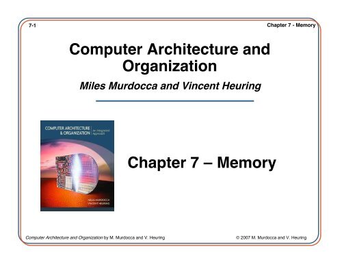
7-1 <strong>Chapter</strong> 7 - <strong>Memory</strong><br />
<strong>Computer</strong> <strong>Architecture</strong> <strong>and</strong><br />
<strong>Organization</strong><br />
Miles Murdocca <strong>and</strong> Vincent Heuring<br />
<strong>Chapter</strong> 7 – <strong>Memory</strong><br />
<strong>Computer</strong> <strong>Architecture</strong> <strong>and</strong> <strong>Organization</strong> by M. Murdocca <strong>and</strong> V. Heuring<br />
© 2007 M. Murdocca <strong>and</strong> V. Heuring
7-2 <strong>Chapter</strong> 7 - <strong>Memory</strong><br />
<strong>Chapter</strong> Contents<br />
7.1 The <strong>Memory</strong> Hierarchy<br />
7.2 R<strong>and</strong>om-Access <strong>Memory</strong><br />
7.3 <strong>Memory</strong> Chip <strong>Organization</strong><br />
7.4 Case Study: Rambus <strong>Memory</strong><br />
7.5 Cache <strong>Memory</strong><br />
7.6 Virtual <strong>Memory</strong><br />
7.7 Advanced Topics<br />
7.8 Case Study: Associative <strong>Memory</strong> in Routers<br />
7.9 Case Study: The Intel Pentium 4 <strong>Memory</strong> System<br />
<strong>Computer</strong> <strong>Architecture</strong> <strong>and</strong> <strong>Organization</strong> by M. Murdocca <strong>and</strong> V. Heuring<br />
© 2007 M. Murdocca <strong>and</strong> V. Heuring
7-3 <strong>Chapter</strong> 7 - <strong>Memory</strong><br />
The <strong>Memory</strong><br />
Hierarchy<br />
<strong>Computer</strong> <strong>Architecture</strong> <strong>and</strong> <strong>Organization</strong> by M. Murdocca <strong>and</strong> V. Heuring<br />
© 2007 M. Murdocca <strong>and</strong> V. Heuring
7-4 <strong>Chapter</strong> 7 - <strong>Memory</strong><br />
Functional Behavior of a RAM Cell<br />
Static RAM cell (a) <strong>and</strong> dynamic RAM cell (b).<br />
<strong>Computer</strong> <strong>Architecture</strong> <strong>and</strong> <strong>Organization</strong> by M. Murdocca <strong>and</strong> V. Heuring<br />
© 2007 M. Murdocca <strong>and</strong> V. Heuring
7-5 <strong>Chapter</strong> 7 - <strong>Memory</strong><br />
Simplified RAM Chip Pinout<br />
<strong>Computer</strong> <strong>Architecture</strong> <strong>and</strong> <strong>Organization</strong> by M. Murdocca <strong>and</strong> V. Heuring<br />
© 2007 M. Murdocca <strong>and</strong> V. Heuring
7-6 <strong>Chapter</strong> 7 - <strong>Memory</strong><br />
A Four-Word<br />
<strong>Memory</strong> with<br />
Four Bits per<br />
Word in a 2D<br />
<strong>Organization</strong><br />
<strong>Computer</strong> <strong>Architecture</strong> <strong>and</strong> <strong>Organization</strong> by M. Murdocca <strong>and</strong> V. Heuring<br />
© 2007 M. Murdocca <strong>and</strong> V. Heuring
7-7 <strong>Chapter</strong> 7 - <strong>Memory</strong><br />
A Simplified Representation of the<br />
Four-Word by Four-Bit RAM<br />
<strong>Computer</strong> <strong>Architecture</strong> <strong>and</strong> <strong>Organization</strong> by M. Murdocca <strong>and</strong> V. Heuring<br />
© 2007 M. Murdocca <strong>and</strong> V. Heuring
7-8 <strong>Chapter</strong> 7 - <strong>Memory</strong><br />
2-1/2D <strong>Organization</strong> of a 64-Word by<br />
One-Bit RAM<br />
<strong>Computer</strong> <strong>Architecture</strong> <strong>and</strong> <strong>Organization</strong> by M. Murdocca <strong>and</strong> V. Heuring<br />
© 2007 M. Murdocca <strong>and</strong> V. Heuring
7-9 <strong>Chapter</strong> 7 - <strong>Memory</strong><br />
Two Four-Word by Four-Bit RAMs are<br />
Used in Creating a Four-Word by<br />
Eight-Bit RAM<br />
<strong>Computer</strong> <strong>Architecture</strong> <strong>and</strong> <strong>Organization</strong> by M. Murdocca <strong>and</strong> V. Heuring<br />
© 2007 M. Murdocca <strong>and</strong> V. Heuring
7-10 <strong>Chapter</strong> 7 - <strong>Memory</strong><br />
Two Four-Word by Four-Bit RAMs Make<br />
up an Eight-Word by Four-Bit RAM<br />
<strong>Computer</strong> <strong>Architecture</strong> <strong>and</strong> <strong>Organization</strong> by M. Murdocca <strong>and</strong> V. Heuring<br />
© 2007 M. Murdocca <strong>and</strong> V. Heuring
7-11 <strong>Chapter</strong> 7 - <strong>Memory</strong><br />
Single-In-Line<br />
<strong>Memory</strong><br />
Module<br />
• 256 MB dual in-line<br />
memory module organized<br />
for a 64-bit word with 16<br />
16M × 8-bit RAM chips<br />
(eight chips on each side<br />
of the DIMM).<br />
<strong>Computer</strong> <strong>Architecture</strong> <strong>and</strong> <strong>Organization</strong> by M. Murdocca <strong>and</strong> V. Heuring<br />
© 2007 M. Murdocca <strong>and</strong> V. Heuring
7-12 <strong>Chapter</strong> 7 - <strong>Memory</strong><br />
Single-In-<br />
Line <strong>Memory</strong><br />
Module<br />
• Schematic diagram of<br />
256 MB dual in-line<br />
memory module.<br />
(Source: adapted from<br />
http://wwws.ti.com/sc/ds/tm4en64<br />
kpu.pdf.)<br />
<strong>Computer</strong> <strong>Architecture</strong> <strong>and</strong> <strong>Organization</strong> by M. Murdocca <strong>and</strong> V. Heuring<br />
© 2007 M. Murdocca <strong>and</strong> V. Heuring
7-13 <strong>Chapter</strong> 7 - <strong>Memory</strong><br />
A ROM Stores Four Four-Bit Words<br />
<strong>Computer</strong> <strong>Architecture</strong> <strong>and</strong> <strong>Organization</strong> by M. Murdocca <strong>and</strong> V. Heuring<br />
© 2007 M. Murdocca <strong>and</strong> V. Heuring
7-14 <strong>Chapter</strong> 7 - <strong>Memory</strong><br />
A Lookup Table (LUT) Implements an<br />
Eight-Bit ALU<br />
<strong>Computer</strong> <strong>Architecture</strong> <strong>and</strong> <strong>Organization</strong> by M. Murdocca <strong>and</strong> V. Heuring<br />
© 2007 M. Murdocca <strong>and</strong> V. Heuring
7-15 <strong>Chapter</strong> 7 - <strong>Memory</strong><br />
Flash <strong>Memory</strong><br />
• (a) External view of flash memory module <strong>and</strong> (b) flash module<br />
internals. (Source: adapted from HowStuffWorks.com.)<br />
<strong>Computer</strong> <strong>Architecture</strong> <strong>and</strong> <strong>Organization</strong> by M. Murdocca <strong>and</strong> V. Heuring<br />
© 2007 M. Murdocca <strong>and</strong> V. Heuring
7-16 <strong>Chapter</strong> 7 - <strong>Memory</strong><br />
Cell Structure for Flash <strong>Memory</strong><br />
• Current flows from source to drain when a sufficient negative charge is<br />
placed on the dielectric material, preventing current flow through the<br />
word line. This is the logical 0 state. When the dielectric material is not<br />
charged, current flows between the bit <strong>and</strong> word lines, which is the<br />
logical 1 state.<br />
<strong>Computer</strong> <strong>Architecture</strong> <strong>and</strong> <strong>Organization</strong> by M. Murdocca <strong>and</strong> V. Heuring<br />
© 2007 M. Murdocca <strong>and</strong> V. Heuring
7-17 <strong>Chapter</strong> 7 - <strong>Memory</strong><br />
Rambus <strong>Memory</strong><br />
• Comparison of DRAM <strong>and</strong> RDRAM configurations.<br />
<strong>Computer</strong> <strong>Architecture</strong> <strong>and</strong> <strong>Organization</strong> by M. Murdocca <strong>and</strong> V. Heuring<br />
© 2007 M. Murdocca <strong>and</strong> V. Heuring
7-18 <strong>Chapter</strong> 7 - <strong>Memory</strong><br />
Rambus <strong>Memory</strong><br />
• Rambus technology on the Nintendo 64 motherboard (left)<br />
enables cost savings over the conventional Sega Saturn<br />
motherboard design (right).<br />
• Nintendo 64 game console:<br />
<strong>Computer</strong> <strong>Architecture</strong> <strong>and</strong> <strong>Organization</strong> by M. Murdocca <strong>and</strong> V. Heuring<br />
© 2007 M. Murdocca <strong>and</strong> V. Heuring
7-19 <strong>Chapter</strong> 7 - <strong>Memory</strong><br />
Placement of Cache <strong>Memory</strong> in a<br />
<strong>Computer</strong> System<br />
• The locality principle: a recently referenced memory location is likely to<br />
be referenced again (temporal locality); a neighbor of a recently<br />
referenced memory location is likely to be referenced (spatial locality).<br />
<strong>Computer</strong> <strong>Architecture</strong> <strong>and</strong> <strong>Organization</strong> by M. Murdocca <strong>and</strong> V. Heuring<br />
© 2007 M. Murdocca <strong>and</strong> V. Heuring
7-20 <strong>Chapter</strong> 7 - <strong>Memory</strong><br />
An Associative Mapping Scheme for a<br />
Cache <strong>Memory</strong><br />
<strong>Computer</strong> <strong>Architecture</strong> <strong>and</strong> <strong>Organization</strong> by M. Murdocca <strong>and</strong> V. Heuring<br />
© 2007 M. Murdocca <strong>and</strong> V. Heuring
7-21 <strong>Chapter</strong> 7 - <strong>Memory</strong><br />
Associative Mapping Example<br />
• Consider how an access to memory location (A035F014) 16 is mapped to<br />
the cache for a 2 32 word memory. The memory is divided into 2 27 blocks<br />
of 2 5 = 32 words per block, <strong>and</strong> the cache consists of 2 14 slots:<br />
• If the addressed word is in the cache, it will be found in word (14) 16 of a<br />
slot that has tag (501AF80) 16 , which is made up of the 27 most<br />
significant bits of the address. If the addressed word is not in the<br />
cache, then the block corresponding to tag field (501AF80) 16 is brought<br />
into an available slot in the cache from the main memory, <strong>and</strong> the<br />
memory reference is then satisfied from the cache.<br />
<strong>Computer</strong> <strong>Architecture</strong> <strong>and</strong> <strong>Organization</strong> by M. Murdocca <strong>and</strong> V. Heuring<br />
© 2007 M. Murdocca <strong>and</strong> V. Heuring
7-22 <strong>Chapter</strong> 7 - <strong>Memory</strong><br />
Associative Mapping Area Allocation<br />
• Area allocation for associative mapping scheme based on bits stored:<br />
<strong>Computer</strong> <strong>Architecture</strong> <strong>and</strong> <strong>Organization</strong> by M. Murdocca <strong>and</strong> V. Heuring<br />
© 2007 M. Murdocca <strong>and</strong> V. Heuring
7-23 <strong>Chapter</strong> 7 - <strong>Memory</strong><br />
Replacement Policies<br />
• When there are no available slots in which to place a block, a<br />
replacement policy is implemented. The replacement policy governs<br />
the choice of which slot is freed up for the new block.<br />
• Replacement policies are used for associative <strong>and</strong> set-associative<br />
mapping schemes, <strong>and</strong> also for virtual memory.<br />
• Least recently used (LRU)<br />
• First-in/first-out (FIFO)<br />
• Least frequently used (LFU)<br />
• R<strong>and</strong>om<br />
• Optimal (used for analysis only – look backward in time <strong>and</strong> reverseengineer<br />
the best possible strategy for a particular sequence of<br />
memory references.)<br />
<strong>Computer</strong> <strong>Architecture</strong> <strong>and</strong> <strong>Organization</strong> by M. Murdocca <strong>and</strong> V. Heuring<br />
© 2007 M. Murdocca <strong>and</strong> V. Heuring
7-24 <strong>Chapter</strong> 7 - <strong>Memory</strong><br />
A Direct Mapping Scheme for Cache<br />
<strong>Memory</strong><br />
<strong>Computer</strong> <strong>Architecture</strong> <strong>and</strong> <strong>Organization</strong> by M. Murdocca <strong>and</strong> V. Heuring<br />
© 2007 M. Murdocca <strong>and</strong> V. Heuring
7-25 <strong>Chapter</strong> 7 - <strong>Memory</strong><br />
Direct Mapping Example<br />
• For a direct mapped cache, each main memory block can be mapped to<br />
only one slot, but each slot can receive more than one block. Consider<br />
how an access to memory location (A035F014) 16 is mapped to the<br />
cache for a 2 32 word memory. The memory is divided into 2 27 blocks of<br />
2 5 = 32 words per block, <strong>and</strong> the cache consists of 2 14 slots:<br />
• If the addressed word is in the cache, it will be found in word (14) 16 of slot<br />
(2F80) 16 , which will have a tag of (1406) 16 .<br />
<strong>Computer</strong> <strong>Architecture</strong> <strong>and</strong> <strong>Organization</strong> by M. Murdocca <strong>and</strong> V. Heuring<br />
© 2007 M. Murdocca <strong>and</strong> V. Heuring
7-26 <strong>Chapter</strong> 7 - <strong>Memory</strong><br />
Direct Mapping Area Allocation<br />
• Area allocation for direct mapping scheme based on bits stored:<br />
<strong>Computer</strong> <strong>Architecture</strong> <strong>and</strong> <strong>Organization</strong> by M. Murdocca <strong>and</strong> V. Heuring<br />
© 2007 M. Murdocca <strong>and</strong> V. Heuring
7-27 <strong>Chapter</strong> 7 - <strong>Memory</strong><br />
A Set Associative Mapping Scheme<br />
for a Cache <strong>Memory</strong><br />
<strong>Computer</strong> <strong>Architecture</strong> <strong>and</strong> <strong>Organization</strong> by M. Murdocca <strong>and</strong> V. Heuring<br />
© 2007 M. Murdocca <strong>and</strong> V. Heuring
7-28 <strong>Chapter</strong> 7 - <strong>Memory</strong><br />
Set-Associative Mapping Example<br />
• Consider how an access to memory location (A035F014) 16 is mapped to<br />
the cache for a 2 32 word memory. The memory is divided into 2 27 blocks<br />
of 2 5 = 32 words per block, there are two blocks per set, <strong>and</strong> the cache<br />
consists of 2 14 slots:<br />
• The leftmost 14 bits form the tag field, followed by 13 bits for the set field,<br />
followed by five bits for the word field:<br />
<strong>Computer</strong> <strong>Architecture</strong> <strong>and</strong> <strong>Organization</strong> by M. Murdocca <strong>and</strong> V. Heuring<br />
© 2007 M. Murdocca <strong>and</strong> V. Heuring
7-29 <strong>Chapter</strong> 7 - <strong>Memory</strong><br />
Set Associative Mapping Area<br />
Allocation<br />
• Area allocation for set associative mapping scheme based on bits stored:<br />
<strong>Computer</strong> <strong>Architecture</strong> <strong>and</strong> <strong>Organization</strong> by M. Murdocca <strong>and</strong> V. Heuring<br />
© 2007 M. Murdocca <strong>and</strong> V. Heuring
7-30 <strong>Chapter</strong> 7 - <strong>Memory</strong><br />
Cache Read <strong>and</strong> Write Policies<br />
<strong>Computer</strong> <strong>Architecture</strong> <strong>and</strong> <strong>Organization</strong> by M. Murdocca <strong>and</strong> V. Heuring<br />
© 2007 M. Murdocca <strong>and</strong> V. Heuring
7-31 <strong>Chapter</strong> 7 - <strong>Memory</strong><br />
Hit Ratios <strong>and</strong> Effective Access Times<br />
• Hit ratio <strong>and</strong> effective access time for single level cache:<br />
• Hit ratios <strong>and</strong> effective access time for multi-level cache:<br />
<strong>Computer</strong> <strong>Architecture</strong> <strong>and</strong> <strong>Organization</strong> by M. Murdocca <strong>and</strong> V. Heuring<br />
© 2007 M. Murdocca <strong>and</strong> V. Heuring
7-32 <strong>Chapter</strong> 7 - <strong>Memory</strong><br />
Direct Mapped Cache Example<br />
• Compute hit ratio <strong>and</strong><br />
effective access time for<br />
a program that executes<br />
from memory locations<br />
48 to 95, <strong>and</strong> then loops<br />
10 times from 15 to 31.<br />
• The direct mapped<br />
cache has four 16-word<br />
slots, a hit time of 80 ns,<br />
<strong>and</strong> a miss time of 2500<br />
ns. Load-through is<br />
used. The cache is<br />
initially empty.<br />
<strong>Computer</strong> <strong>Architecture</strong> <strong>and</strong> <strong>Organization</strong> by M. Murdocca <strong>and</strong> V. Heuring<br />
© 2007 M. Murdocca <strong>and</strong> V. Heuring
7-33 <strong>Chapter</strong> 7 - <strong>Memory</strong><br />
Table of Events for Example Program<br />
<strong>Computer</strong> <strong>Architecture</strong> <strong>and</strong> <strong>Organization</strong> by M. Murdocca <strong>and</strong> V. Heuring<br />
© 2007 M. Murdocca <strong>and</strong> V. Heuring
7-34 <strong>Chapter</strong> 7 - <strong>Memory</strong><br />
Calculation of Hit Ratio <strong>and</strong> Effective<br />
Access Time for Example Program<br />
<strong>Computer</strong> <strong>Architecture</strong> <strong>and</strong> <strong>Organization</strong> by M. Murdocca <strong>and</strong> V. Heuring<br />
© 2007 M. Murdocca <strong>and</strong> V. Heuring
7-35 <strong>Chapter</strong> 7 - <strong>Memory</strong><br />
Multi-level Cache <strong>Memory</strong><br />
As an example, consider a two-level cache in which the L1 hit time is 5 ns,<br />
the L2 hit time is 20 ns, <strong>and</strong> the L2 miss time is 100 ns. There are 10,000<br />
memory references of which 10 cause L2 misses <strong>and</strong> 90 cause L1 misses.<br />
Compute the hit ratios of the L1 <strong>and</strong> L2 caches <strong>and</strong> the overall effective<br />
access time.<br />
H 1 is the ratio of the number of times the accessed word is in the L1 cache<br />
to the total number of memory accesses. There are a total of 85 (L1) <strong>and</strong><br />
15 (L2) misses, <strong>and</strong> so:<br />
(Continued on next slide.)<br />
<strong>Computer</strong> <strong>Architecture</strong> <strong>and</strong> <strong>Organization</strong> by M. Murdocca <strong>and</strong> V. Heuring<br />
© 2007 M. Murdocca <strong>and</strong> V. Heuring
7-36 <strong>Chapter</strong> 7 - <strong>Memory</strong><br />
Multi-level Cache <strong>Memory</strong> (Cont’)<br />
H 2 is the ratio of the number of times the accessed word is in the L2 cache<br />
to the number of times the L2 cache is accessed, <strong>and</strong> so:<br />
The effective access time is then:<br />
= 5.23 ns per access<br />
<strong>Computer</strong> <strong>Architecture</strong> <strong>and</strong> <strong>Organization</strong> by M. Murdocca <strong>and</strong> V. Heuring<br />
© 2007 M. Murdocca <strong>and</strong> V. Heuring
7-37 <strong>Chapter</strong> 7 - <strong>Memory</strong><br />
Neat Little LRU Algorithm<br />
• A sequence is shown for the Neat Little LRU Algorithm for a cache with<br />
four slots. Main memory blocks are accessed in the sequence: 0, 2, 3,<br />
1, 5, 4.<br />
<strong>Computer</strong> <strong>Architecture</strong> <strong>and</strong> <strong>Organization</strong> by M. Murdocca <strong>and</strong> V. Heuring<br />
© 2007 M. Murdocca <strong>and</strong> V. Heuring
7-38 <strong>Chapter</strong> 7 - <strong>Memory</strong><br />
Cache Coherency<br />
• The goal of cache coherence is to ensure that every cache sees the<br />
same value for a referenced location, which means making sure that<br />
any shared oper<strong>and</strong> that is changed is updated throughout the system.<br />
• This brings us to the issue of false sharing, which reduces cache<br />
performance when two oper<strong>and</strong>s that are not shared between<br />
processes share the same cache line. The situation is shown below.<br />
The problem is that each process will invalidate the other’s cache line<br />
when writing data without a real need, unless the compiler prevents this.<br />
<strong>Computer</strong> <strong>Architecture</strong> <strong>and</strong> <strong>Organization</strong> by M. Murdocca <strong>and</strong> V. Heuring<br />
© 2007 M. Murdocca <strong>and</strong> V. Heuring
7-39 <strong>Chapter</strong> 7 - <strong>Memory</strong><br />
Overlays<br />
• A partition graph for a program with a main routine <strong>and</strong> three subroutines:<br />
<strong>Computer</strong> <strong>Architecture</strong> <strong>and</strong> <strong>Organization</strong> by M. Murdocca <strong>and</strong> V. Heuring<br />
© 2007 M. Murdocca <strong>and</strong> V. Heuring
7-40 <strong>Chapter</strong> 7 - <strong>Memory</strong><br />
Virtual <strong>Memory</strong><br />
• Virtual memory is stored in a hard disk image. The physical memory<br />
holds a small number of virtual pages in physical page frames.<br />
• A mapping between a virtual <strong>and</strong> a physical memory:<br />
<strong>Computer</strong> <strong>Architecture</strong> <strong>and</strong> <strong>Organization</strong> by M. Murdocca <strong>and</strong> V. Heuring<br />
© 2007 M. Murdocca <strong>and</strong> V. Heuring
7-41 <strong>Chapter</strong> 7 - <strong>Memory</strong><br />
Page Table<br />
• The page table maps between virtual memory <strong>and</strong> physical memory.<br />
<strong>Computer</strong> <strong>Architecture</strong> <strong>and</strong> <strong>Organization</strong> by M. Murdocca <strong>and</strong> V. Heuring<br />
© 2007 M. Murdocca <strong>and</strong> V. Heuring
7-42 <strong>Chapter</strong> 7 - <strong>Memory</strong><br />
Using the Page Table<br />
• A virtual address is<br />
translated into a physical<br />
address:<br />
Typical page table entry<br />
<strong>Computer</strong> <strong>Architecture</strong> <strong>and</strong> <strong>Organization</strong> by M. Murdocca <strong>and</strong> V. Heuring<br />
© 2007 M. Murdocca <strong>and</strong> V. Heuring
7-43 <strong>Chapter</strong> 7 - <strong>Memory</strong><br />
Using the Page Table (cont’)<br />
• The<br />
configuration of<br />
a page table<br />
changes as a<br />
program<br />
executes.<br />
• Initially, the page<br />
table is empty.<br />
In the final<br />
configuration,<br />
four pages are in<br />
physical<br />
memory.<br />
<strong>Computer</strong> <strong>Architecture</strong> <strong>and</strong> <strong>Organization</strong> by M. Murdocca <strong>and</strong> V. Heuring<br />
© 2007 M. Murdocca <strong>and</strong> V. Heuring
7-44 <strong>Chapter</strong> 7 - <strong>Memory</strong><br />
Segmentation<br />
• A segmented memory allows two users to share the same word<br />
processor code, with different data spaces:<br />
<strong>Computer</strong> <strong>Architecture</strong> <strong>and</strong> <strong>Organization</strong> by M. Murdocca <strong>and</strong> V. Heuring<br />
© 2007 M. Murdocca <strong>and</strong> V. Heuring
7-45 <strong>Chapter</strong> 7 - <strong>Memory</strong><br />
Fragmentation<br />
• (a) Free area<br />
of memory<br />
after initialization;<br />
(b)<br />
after<br />
fragmentation;<br />
(c)<br />
after<br />
coalescing.<br />
<strong>Computer</strong> <strong>Architecture</strong> <strong>and</strong> <strong>Organization</strong> by M. Murdocca <strong>and</strong> V. Heuring<br />
© 2007 M. Murdocca <strong>and</strong> V. Heuring
7-46 <strong>Chapter</strong> 7 - <strong>Memory</strong><br />
Translation Lookaside Buffer<br />
• An example TLB holds 8 entries for a system with 32 virtual pages <strong>and</strong><br />
16 page frames.<br />
<strong>Computer</strong> <strong>Architecture</strong> <strong>and</strong> <strong>Organization</strong> by M. Murdocca <strong>and</strong> V. Heuring<br />
© 2007 M. Murdocca <strong>and</strong> V. Heuring
7-47 <strong>Chapter</strong> 7 - <strong>Memory</strong><br />
Putting it All Together<br />
• An example TLB holds 8 entries for a system with 32 virtual pages <strong>and</strong><br />
16 page frames.<br />
<strong>Computer</strong> <strong>Architecture</strong> <strong>and</strong> <strong>Organization</strong> by M. Murdocca <strong>and</strong> V. Heuring<br />
© 2007 M. Murdocca <strong>and</strong> V. Heuring
7-48 <strong>Chapter</strong> 7 - <strong>Memory</strong><br />
Content Addressable <strong>Memory</strong> –<br />
Addressing<br />
• Relationships between r<strong>and</strong>om access memory <strong>and</strong> content<br />
addressable memory:<br />
<strong>Computer</strong> <strong>Architecture</strong> <strong>and</strong> <strong>Organization</strong> by M. Murdocca <strong>and</strong> V. Heuring<br />
© 2007 M. Murdocca <strong>and</strong> V. Heuring
7-49 <strong>Chapter</strong> 7 - <strong>Memory</strong><br />
Overview of CAM<br />
• Source: (Foster,<br />
C. C., Content<br />
Addressable<br />
Parallel<br />
Processors, Van<br />
Nostr<strong>and</strong><br />
Reinhold<br />
Company, 1976.)<br />
<strong>Computer</strong> <strong>Architecture</strong> <strong>and</strong> <strong>Organization</strong> by M. Murdocca <strong>and</strong> V. Heuring<br />
© 2007 M. Murdocca <strong>and</strong> V. Heuring
7-50 <strong>Chapter</strong> 7 - <strong>Memory</strong><br />
Addressing Subtrees for a CAM<br />
<strong>Computer</strong> <strong>Architecture</strong> <strong>and</strong> <strong>Organization</strong> by M. Murdocca <strong>and</strong> V. Heuring<br />
© 2007 M. Murdocca <strong>and</strong> V. Heuring
7-51 <strong>Chapter</strong> 7 - <strong>Memory</strong><br />
Associative <strong>Memory</strong> in Routers<br />
• A simple network with<br />
three routers.<br />
• The use of associative<br />
memories in high-end routers<br />
reduces the lookup time by<br />
allowing a search to be performed in a single operation.<br />
• The search is based on the destination address, rather than the<br />
physical memory address.<br />
• Access methods for this memory have been st<strong>and</strong>ardized into an<br />
interface interoperability agreement by the Network Processing Forum.<br />
<strong>Computer</strong> <strong>Architecture</strong> <strong>and</strong> <strong>Organization</strong> by M. Murdocca <strong>and</strong> V. Heuring<br />
© 2007 M. Murdocca <strong>and</strong> V. Heuring
7-52 <strong>Chapter</strong> 7 - <strong>Memory</strong><br />
Block Diagram of Dual-Read RAM<br />
• A dual-read or dual-port<br />
RAM allows any two<br />
words to be<br />
simultaneously read<br />
from the same memory.<br />
<strong>Computer</strong> <strong>Architecture</strong> <strong>and</strong> <strong>Organization</strong> by M. Murdocca <strong>and</strong> V. Heuring<br />
© 2007 M. Murdocca <strong>and</strong> V. Heuring
7-53 <strong>Chapter</strong> 7 - <strong>Memory</strong><br />
The Intel 4 Pentium <strong>Memory</strong> System<br />
<strong>Computer</strong> <strong>Architecture</strong> <strong>and</strong> <strong>Organization</strong> by M. Murdocca <strong>and</strong> V. Heuring<br />
© 2007 M. Murdocca <strong>and</strong> V. Heuring


