CIN::APSE Design Guide - Cinch Connectors
CIN::APSE Design Guide - Cinch Connectors
CIN::APSE Design Guide - Cinch Connectors

You also want an ePaper? Increase the reach of your titles
YUMPU automatically turns print PDFs into web optimized ePapers that Google loves.
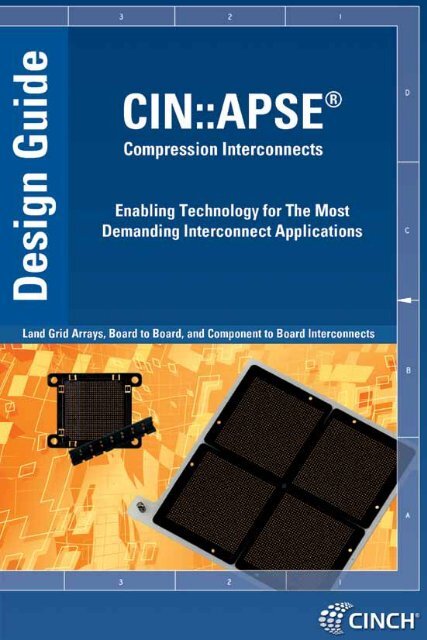
Welcome<br />
This guide has been designed to familiarize you with <strong>CIN</strong>::<strong>APSE</strong> ® - the unique, high-performance,<br />
solderless interconnect solution - and to guide you in using <strong>CIN</strong>::<strong>APSE</strong> ® in your applications.<br />
Table of Contents<br />
Technology Page 2<br />
Applications Page 3<br />
Configurations Page 4-5<br />
Force Deflection Resistance Curve Page 5<br />
<strong>Design</strong> <strong>Guide</strong>lines Page 6<br />
Compression Systems Page 7<br />
Performance Characteristics Page 8<br />
<strong>CIN</strong>::<strong>APSE</strong> ®<br />
Technology<br />
<strong>CIN</strong>::<strong>APSE</strong> ® is a solderless Z-axis interconnect technology that offers exceptional mechanical and<br />
electrical performance. Custom made to your specifications, <strong>CIN</strong>::<strong>APSE</strong> ® utilizes a multi-point contact<br />
that can handle signals well above 20 GHz, while offering a superior combination of small size,<br />
low inductance, and exceptional resistance to shock,<br />
vibration and thermal cycling.<br />
2<br />
Connector Cross Section Showing<br />
<strong>CIN</strong>::<strong>APSE</strong> ® Contact<br />
The key to this highly innovative technology is the<br />
<strong>CIN</strong>::<strong>APSE</strong> ® contact (shown left). The contacts, which<br />
are made from randomly wound gold plated molybdenum<br />
wire, are loaded into a plastic insulator engineered<br />
to the exact requirements of the application.<br />
<strong>Cinch</strong>’s patented hourglass hole design retains the<br />
contact and allows the contact to float in the insulator,<br />
while maintaining contact even under extreme thermal<br />
expansion mismatches between mated substrates.
<strong>CIN</strong>::<strong>APSE</strong> ®<br />
Applications<br />
<strong>CIN</strong>::<strong>APSE</strong> ® can be used in almost any application<br />
where you need to connect two parallel surfaces.<br />
Common applications include:<br />
• Board to Board<br />
• Chip Package to Board/Land Grid Array (LGA)<br />
• Flex to Board<br />
• Component to Board<br />
Board to Board<br />
Chip Package to Board<br />
Flex to Board<br />
Component to Board<br />
3
<strong>CIN</strong>::<strong>APSE</strong> ®<br />
Configurations<br />
By using different sizes of contacts, plungers, and spacers, a wide range of contact configurations<br />
can be created. To choose the one that best fits your application, consider the examples given<br />
below in conjunction with your mating requirements and Z-axis height.<br />
4<br />
Contact Only<br />
This <strong>CIN</strong>::<strong>APSE</strong> ® configuration provides multiple points of<br />
contact and mechanical wipe. It is ideally suited for<br />
applications requiring high speed, low profile, and high<br />
density. LGA sockets and flex to board interconnects commonly<br />
use this configuration.<br />
Plunger-Contact<br />
The addition of a plunger increases the handling durability of<br />
the <strong>CIN</strong>::<strong>APSE</strong> ® contacts and provides additional height. This<br />
configuration is well-matched for board to board and test<br />
applications.<br />
Plunger-Contact-Plunger<br />
Adding a second plunger to the connector results in a tall<br />
system - up to 1.0” [25.4mm] - that is also the most durable in terms<br />
of handling. This configuration is best suited for contacts that have<br />
excessive handling from both sides. It is generally used for parallel<br />
board to board stacking connector applications.<br />
Contact-Spacer-Contact<br />
Using two contacts with a spacer in between creates a connector<br />
with all the benefits of the contact only style, and the ability to<br />
span greater Z-axis heights - up to 1.0” [25.4mm]. This configuration<br />
is most often used in high shock and vibration environments,<br />
when multiple points of contact are needed in a tall connector.
Mated Height Range for Different Configurations<br />
Typical Curve for a 0.020” Dia. Contact in an Insulator 0.032” [0.81] thick<br />
5
<strong>Design</strong> <strong>Guide</strong>lines<br />
Here are some basic guidelines to follow when laying out your PCB, flex circuit or chip package to<br />
work with the <strong>CIN</strong>::<strong>APSE</strong> ® contacts.<br />
6<br />
1. Ensure that mated height stays within specified range. (pg. 5)<br />
2. Gold interfaces are needed on contact surfaces being mated. (below)<br />
3. Compression must be applied and maintained within the specified range. (pg. 5)<br />
A compression system may be required. (pg. 7)<br />
4. The operating environment (temperature) must be compatible<br />
with the contact and insulator material. (pg. 8)<br />
General Configuration <strong>Guide</strong>lines<br />
Pad Plating 15-30 µin Au over 50 µin Ni<br />
(Depending on the application, less gold has been successfully used)<br />
In-Pad Vias Open vias allowable; Maximum diameter of 0.010” [0.25mm]<br />
(for contact only configurations)<br />
PCB/Chip Flatness 0.003” [0.08mm] per side / 0.006” [0.16 mm] total<br />
Pad true position Typically 0.008” [0.20 mm]<br />
Specific Configuration <strong>Guide</strong>lines (in inches [mm] and ounces [g])<br />
Characteristics Contact Only<br />
f 0.020”<br />
[0.508]<br />
Contact<br />
- Plunger<br />
Plunger<br />
- Contact<br />
- Plunger<br />
Contact<br />
- Spacer<br />
- Contact<br />
Contact Only<br />
f 0.040”<br />
[1.02]<br />
Pad Size (+/- 0.003”) 0.027” [0.69] 0.027” [0.69] 0.020” [0.51] 0.027” [0.69] 0.054” [1.37]<br />
Min. Center-Spacing 0.040” [1.00] 0.050” [1.27] 0.050” [1.27] 0.050” [1.27] 0.070” [1.78]<br />
Min. Compression* 2.5 oz 2.5 oz 2.5 oz 2.5 oz 4 oz<br />
Force/contact<br />
[71] [71] [71] [71] [113]<br />
Working Compression<br />
Range<br />
0-0.006”<br />
[0.15]<br />
0-0.006”<br />
[0.15]<br />
0-0.010”<br />
[0.25]<br />
<strong>CIN</strong>::<strong>APSE</strong> ®<br />
Materials<br />
Contact Gold plated molybdenum<br />
Spacer Gold plated brass or copper alloy<br />
Plunger Gold plated brass or copper alloy<br />
Insulator Housing - Molded Liquid Crystal Polymer or Ultem<br />
Insulator Housing - Machined Ultem or Torlon<br />
Packaging Trays Antistat ABS<br />
0-0.012”<br />
[0.30]<br />
0-0.008”<br />
[0.20]<br />
* For reference only. Compression force depends on number of contacts and insulator geometry used in an application.<br />
Contact <strong>Cinch</strong> before starting your design to verify the optimal compression force for your design.
<strong>CIN</strong>::<strong>APSE</strong> ®<br />
Compression Systems<br />
<strong>CIN</strong>::<strong>APSE</strong> ® applications typically require<br />
a compression system, which uniformly<br />
distributes force throughout the<br />
connector, and ensures adequate<br />
planarity.<br />
Compression systems can range<br />
from simple fasteners or<br />
screws to more<br />
sophisticated systems<br />
as the I/O count increases.<br />
Flex Circuit Compression System<br />
LGA Compression System<br />
Threaded hardware with<br />
controlled stop: provides<br />
pre-established compression<br />
to the springs and transfers<br />
load to the system.<br />
Springs (ground ended, with<br />
known spring rate): to assure<br />
a uniform load distribution.<br />
Heatsink with bolster plate:<br />
for support and planarity.<br />
Flex Circuit<br />
<strong>Cinch</strong> has years of experience in designing compression systems for <strong>CIN</strong>::<strong>APSE</strong> ® applications.<br />
Please contact us to help optimize a compression system to meet your specific application. 7<br />
PCB<br />
Bolster plate
Typical Performance Characteristics<br />
* Test results are pass/fail criteria, not limitations of the technology. Results are for typical applications.<br />
Contact <strong>Cinch</strong> to discuss specific applications.<br />
8<br />
Electrical* (at full compression)<br />
Characteristics Contact Only Contact<br />
- Plunger<br />
f 0.020” [0.50] f 0.040” [1.00]<br />
Plunger<br />
- Contact<br />
- Plunger<br />
Contact<br />
- Spacer<br />
- Contact<br />
Contact Only<br />
Contact Resistance