- Page 2:
MODERN SPECTROSCOPY Fourth Edition
- Page 8:
Copyright # 1987, 1992, 1996, 2004
- Page 12:
vi CONTENTS Exercises 38 Bibliograp
- Page 16:
viii CONTENTS 6.1.4 Vibration-rotat
- Page 20:
x CONTENTS 8.2.1.2 Processes in Aug
- Page 26:
Preface to first edition Modern Spe
- Page 30:
Preface to second edition A new edi
- Page 34:
Preface to third edition One of the
- Page 38:
Preface to fourth edition Spectrosc
- Page 42:
Units, dimensions and conventions T
- Page 46:
UNITS, DIMENSIONS AND CONVENTIONS x
- Page 54:
Useful Conversion Factors Unit cm 7
- Page 62:
1 Some Important Results in Quantum
- Page 66:
1.2 THE EVOLUTION OF QUANTUM THEORY
- Page 70:
levels in Figure 1.1 except that ~n
- Page 74:
1.2 THE EVOLUTION OF QUANTUM THEORY
- Page 78:
1.3 THE SCHRÖDINGER EQUATION AND S
- Page 82:
1.3 THE SCHRÖDINGER EQUATION AND S
- Page 86:
Table 1.1 Some Y ‘m‘ wave funct
- Page 90:
3. Plot 4pr2R2 n‘ against r (or r
- Page 94:
1.3 THE SCHRÖDINGER EQUATION AND S
- Page 98:
Table 1.3 Some values of the nuclea
- Page 102:
1.3.5 The rigid rotor 1.3 THE SCHR
- Page 106:
1.3 THE SCHRÖDINGER EQUATION AND S
- Page 110:
the molecule may have even at the a
- Page 114:
2 Electromagnetic Radiation and its
- Page 118:
2.2 ABSORPTION AND EMISSION OF RADI
- Page 122:
For the vibrational energy level: N
- Page 126:
2.2 ABSORPTION AND EMISSION OF RADI
- Page 130:
Here, t is the time taken for N n t
- Page 134:
although, as we shall see in Chapte
- Page 138:
2.2 Calculate in hertz the broadeni
- Page 144:
42 3 GENERAL FEATURES OF EXPERIMENT
- Page 148:
44 3 GENERAL FEATURES OF EXPERIMENT
- Page 152:
46 3 GENERAL FEATURES OF EXPERIMENT
- Page 156:
48 3 GENERAL FEATURES OF EXPERIMENT
- Page 160:
50 3 GENERAL FEATURES OF EXPERIMENT
- Page 164:
52 3 GENERAL FEATURES OF EXPERIMENT
- Page 168:
54 3 GENERAL FEATURES OF EXPERIMENT
- Page 172:
56 3 GENERAL FEATURES OF EXPERIMENT
- Page 176:
58 3 GENERAL FEATURES OF EXPERIMENT
- Page 180:
60 3 GENERAL FEATURES OF EXPERIMENT
- Page 184:
62 3 GENERAL FEATURES OF EXPERIMENT
- Page 188:
64 3 GENERAL FEATURES OF EXPERIMENT
- Page 192:
66 3 GENERAL FEATURES OF EXPERIMENT
- Page 196:
68 3 GENERAL FEATURES OF EXPERIMENT
- Page 200:
70 3 GENERAL FEATURES OF EXPERIMENT
- Page 206:
4 Molecular Symmetry The theory of
- Page 210:
4.1.2 Plane of symmetry, s 4.1 ELEM
- Page 214:
plane. This example also illustrate
- Page 218:
4.1 ELEMENTS OF SYMMETRY 79 racemic
- Page 222:
All the other four structures in Fi
- Page 226:
4.2.2 S n point groups An Sn point
- Page 230:
(Figure 4.11j), for example, and al
- Page 234:
Molecules belonging to the I h poin
- Page 238:
4.3 POINT GROUP CHARACTER TABLES 89
- Page 242:
4.3 POINT GROUP CHARACTER TABLES 91
- Page 246:
4.3 POINT GROUP CHARACTER TABLES 93
- Page 250:
4.3 POINT GROUP CHARACTER TABLES 95
- Page 254:
4.3.4 I h character table The I h c
- Page 258:
In molecules such as trans-1,2-difl
- Page 262:
(b) F I, s H F Point group Cs δ +
- Page 266:
5 Rotational Spectroscopy 5.1 Linea
- Page 270:
5.2 ROTATIONAL INFRARED, MILLIMETRE
- Page 274:
5.2 ROTATIONAL INFRARED, MILLIMETRE
- Page 278:
5.2 ROTATIONAL INFRARED, MILLIMETRE
- Page 282:
5.2 ROTATIONAL INFRARED, MILLIMETRE
- Page 286:
5.2 ROTATIONAL INFRARED, MILLIMETRE
- Page 290:
5.2 ROTATIONAL INFRARED, MILLIMETRE
- Page 294:
5.2 ROTATIONAL INFRARED, MILLIMETRE
- Page 298:
5.2 ROTATIONAL INFRARED, MILLIMETRE
- Page 302:
5.2 ROTATIONAL INFRARED, MILLIMETRE
- Page 306:
5.3 ROTATIONAL RAMAN SPECTROSCOPY 1
- Page 310:
5.3 ROTATIONAL RAMAN SPECTROSCOPY 1
- Page 314:
5.3 ROTATIONAL RAMAN SPECTROSCOPY 1
- Page 318:
5.3 ROTATIONAL RAMAN SPECTROSCOPY 1
- Page 322:
5.4 STRUCTURE DETERMINATION FROM RO
- Page 326:
5.4 STRUCTURE DETERMINATION FROM RO
- Page 330:
5.2 Rearrange Equation (5.20) into
- Page 336:
138 6 VIBRATIONAL SPECTROSCOPY Tabl
- Page 340:
140 6 VIBRATIONAL SPECTROSCOPY Figu
- Page 344:
142 6 VIBRATIONAL SPECTROSCOPY temp
- Page 348:
144 6 VIBRATIONAL SPECTROSCOPY wher
- Page 352:
146 6 VIBRATIONAL SPECTROSCOPY tran
- Page 356:
148 6 VIBRATIONAL SPECTROSCOPY Figu
- Page 360:
150 6 VIBRATIONAL SPECTROSCOPY From
- Page 364:
152 6 VIBRATIONAL SPECTROSCOPY Figu
- Page 368:
154 6 VIBRATIONAL SPECTROSCOPY purp
- Page 372:
156 6 VIBRATIONAL SPECTROSCOPY Figu
- Page 376:
158 6 VIBRATIONAL SPECTROSCOPY Figu
- Page 380:
160 6 VIBRATIONAL SPECTROSCOPY Figu
- Page 384:
162 6 VIBRATIONAL SPECTROSCOPY has
- Page 388:
164 6 VIBRATIONAL SPECTROSCOPY Tabl
- Page 392:
166 6 VIBRATIONAL SPECTROSCOPY Tabl
- Page 396:
168 6 VIBRATIONAL SPECTROSCOPY just
- Page 400:
170 6 VIBRATIONAL SPECTROSCOPY whic
- Page 404:
172 6 VIBRATIONAL SPECTROSCOPY Acet
- Page 408:
174 6 VIBRATIONAL SPECTROSCOPY wher
- Page 412:
176 6 VIBRATIONAL SPECTROSCOPY Figu
- Page 416:
178 6 VIBRATIONAL SPECTROSCOPY even
- Page 420:
180 6 VIBRATIONAL SPECTROSCOPY Figu
- Page 424:
182 6 VIBRATIONAL SPECTROSCOPY Figu
- Page 428:
184 6 VIBRATIONAL SPECTROSCOPY 6.2.
- Page 432:
186 6 VIBRATIONAL SPECTROSCOPY Figu
- Page 436:
188 6 VIBRATIONAL SPECTROSCOPY This
- Page 440:
190 6 VIBRATIONAL SPECTROSCOPY Figu
- Page 444:
192 6 VIBRATIONAL SPECTROSCOPY The
- Page 448:
194 6 VIBRATIONAL SPECTROSCOPY Figu
- Page 452:
196 6 VIBRATIONAL SPECTROSCOPY 6.2
- Page 458:
7 Electronic Spectroscopy 7.1 Atomi
- Page 462:
Electrons in the atom concerned may
- Page 466:
Table 7.1 (continued ) Atom Z Groun
- Page 470:
7.1.2.2 Coupling of angular momenta
- Page 474:
7.1 ATOMIC SPECTROSCOPY 207 Figure
- Page 478:
7.1 ATOMIC SPECTROSCOPY 209 Table 7
- Page 482:
Table 7.3 Derivation of terms arisi
- Page 486:
7.1.3 Spectra of alkali metal atoms
- Page 490:
7.1 ATOMIC SPECTROSCOPY 215 Some ex
- Page 494:
7.1 ATOMIC SPECTROSCOPY 217 Figure
- Page 498:
Both the calculated wavelengths of
- Page 502:
7.1 ATOMIC SPECTROSCOPY 221 Figure
- Page 506:
An obvious difference between the e
- Page 510:
For the coupling of the orbital ang
- Page 514:
AO is antisymmetric to this reflect
- Page 518:
7.2 ELECTRONIC SPECTROSCOPY OF DIAT
- Page 522:
7.2 ELECTRONIC SPECTROSCOPY OF DIAT
- Page 526:
7.2 ELECTRONIC SPECTROSCOPY OF DIAT
- Page 530:
7.2 ELECTRONIC SPECTROSCOPY OF DIAT
- Page 534:
Rule 4: þ$j ; þ$þ; $ ð7:70Þ Th
- Page 538:
The ground configuration of oxygen
- Page 542:
7.2 ELECTRONIC SPECTROSCOPY OF DIAT
- Page 546:
7.2 ELECTRONIC SPECTROSCOPY OF DIAT
- Page 550:
7.2 ELECTRONIC SPECTROSCOPY OF DIAT
- Page 554:
7.2 ELECTRONIC SPECTROSCOPY OF DIAT
- Page 558:
maximum at v 0 > 0 indicates qualit
- Page 562:
7.2 ELECTRONIC SPECTROSCOPY OF DIAT
- Page 566:
Hence, D 0 0 can be obtained from ~
- Page 570:
7.2 ELECTRONIC SPECTROSCOPY OF DIAT
- Page 574:
7.2 ELECTRONIC SPECTROSCOPY OF DIAT
- Page 578:
7.2 ELECTRONIC SPECTROSCOPY OF DIAT
- Page 582:
For non-linear polyatomic molecules
- Page 586:
7.3 ELECTRONIC SPECTROSCOPY OF POLY
- Page 590:
orbital more than counterbalances t
- Page 594:
7.3.1.3 Benzene 7.3 ELECTRONIC SPEC
- Page 598:
7.3 ELECTRONIC SPECTROSCOPY OF POLY
- Page 602:
7.3 ELECTRONIC SPECTROSCOPY OF POLY
- Page 606:
7.3 ELECTRONIC SPECTROSCOPY OF POLY
- Page 610:
pushed down. The result, as shown i
- Page 614:
for transitions between non-degener
- Page 618:
Gðc 0 vÞ ¼Gðc 00 vÞ in Equatio
- Page 622:
7.3 ELECTRONIC SPECTROSCOPY OF POLY
- Page 626:
7.3 ELECTRONIC SPECTROSCOPY OF POLY
- Page 630:
7.3 ELECTRONIC SPECTROSCOPY OF POLY
- Page 634:
Exercises 7.1 Indicate which of the
- Page 638:
8 Photoelectron and Related Spectro
- Page 642:
Figures 8.1(a) and 8.1(b) illustrat
- Page 646:
8.1 PHOTOELECTRON SPECTROSCOPY 293
- Page 650:
8.1 PHOTOELECTRON SPECTROSCOPY 295
- Page 654:
In most cases of closed-shell molec
- Page 658:
8.1 PHOTOELECTRON SPECTROSCOPY 299
- Page 662:
Figure 8.9 The He I ultraviolet pho
- Page 666:
spectroscopy to be 1.4144 A˚ in th
- Page 670:
8.1 PHOTOELECTRON SPECTROSCOPY 305
- Page 674:
degeneracy. The only relatively sim
- Page 678:
The spectrum below shows that the O
- Page 682:
8.1 PHOTOELECTRON SPECTROSCOPY 311
- Page 686:
Figure 8.17 A short, barely resolve
- Page 690:
8.2 AUGER ELECTRON AND X-RAY FLUORE
- Page 694:
8.2 AUGER ELECTRON AND X-RAY FLUORE
- Page 698:
8.2 AUGER ELECTRON AND X-RAY FLUORE
- Page 702:
8.2 AUGER ELECTRON AND X-RAY FLUORE
- Page 706:
8.2 AUGER ELECTRON AND X-RAY FLUORE
- Page 710: 8.2 AUGER ELECTRON AND X-RAY FLUORE
- Page 714: 8.3 EXTENDED X-RAY ABSORPTION FINE
- Page 718: 8.3 EXTENDED X-RAY ABSORPTION FINE
- Page 722: 8.3 EXTENDED X-RAY ABSORPTION FINE
- Page 726: 8.3 EXTENDED X-RAY ABSORPTION FINE
- Page 730: 8.4 EXAFS spectra of platinum metal
- Page 734: 9 LASERS AND LASER SPECTROSCOPY 9.1
- Page 738: 9.1 GENERAL DISCUSSION OF LASERS 33
- Page 742: The four-level system in Figure 9.2
- Page 746: 9.1 GENERAL DISCUSSION OF LASERS 34
- Page 750: 9.1.6 Harmonic generation In the co
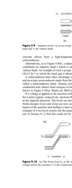
- Page 754: 9.2 EXAMPLES OF LASERS 347 Figure 9
- Page 758: produce pulses as short a 8 fs. Com
- Page 764: 352 9 LASERS AND LASER SPECTROSCOPY
- Page 768: 354 9 LASERS AND LASER SPECTROSCOPY
- Page 772: 356 9 LASERS AND LASER SPECTROSCOPY
- Page 776: 358 9 LASERS AND LASER SPECTROSCOPY
- Page 780: 360 9 LASERS AND LASER SPECTROSCOPY
- Page 784: 362 9 LASERS AND LASER SPECTROSCOPY
- Page 788: 364 9 LASERS AND LASER SPECTROSCOPY
- Page 792: 366 9 LASERS AND LASER SPECTROSCOPY
- Page 796: 368 9 LASERS AND LASER SPECTROSCOPY
- Page 800: 370 9 LASERS AND LASER SPECTROSCOPY
- Page 804: 372 9 LASERS AND LASER SPECTROSCOPY
- Page 808: 374 9 LASERS AND LASER SPECTROSCOPY
- Page 812:
376 9 LASERS AND LASER SPECTROSCOPY
- Page 816:
378 9 LASERS AND LASER SPECTROSCOPY
- Page 820:
380 9 LASERS AND LASER SPECTROSCOPY
- Page 824:
382 9 LASERS AND LASER SPECTROSCOPY
- Page 828:
384 9 LASERS AND LASER SPECTROSCOPY
- Page 832:
386 9 LASERS AND LASER SPECTROSCOPY
- Page 836:
388 9 LASERS AND LASER SPECTROSCOPY
- Page 840:
390 9 LASERS AND LASER SPECTROSCOPY
- Page 844:
392 9 LASERS AND LASER SPECTROSCOPY
- Page 848:
394 9 LASERS AND LASER SPECTROSCOPY
- Page 852:
396 9 LASERS AND LASER SPECTROSCOPY
- Page 856:
398 9 LASERS AND LASER SPECTROSCOPY
- Page 860:
400 9 LASERS AND LASER SPECTROSCOPY
- Page 864:
402 9 LASERS AND LASER SPECTROSCOPY
- Page 868:
404 9 LASERS AND LASER SPECTROSCOPY
- Page 874:
Appendix A Character Tables Index t
- Page 878:
Table A.7 C 5 I C 5 C 2 5 C 3 5 C 4
- Page 882:
Table A.14 C 5v I 2C 5 2C 2 5 5s v
- Page 886:
Table A.22 C 2h I C 2 i s h A g 1 1
- Page 890:
Table A.27 D 2d I 2S 4 C 2 2C 0 2 2
- Page 894:
Table A.33 D 3h I 2C 3 3C 2 s h 2S
- Page 898:
Table A.38 S 4 I S 4 C 2 S 3 4 A 1
- Page 902:
Table A.43 O h I 8C 3 6C 2 6C 4 3C
- Page 906:
Appendix B Symmetry Species of Vibr
- Page 910:
Table B.2 (continued ) Point group
- Page 914:
Table B.2 (continued ) Point group
- Page 918:
Index of Atoms and Molecules The sy
- Page 922:
EXAFS, 329 on graphite, SEXAFS, 333
- Page 926:
TlBr=TlI in attenuated total reflec
- Page 930:
CH 3I (methyl iodide) principal axe
- Page 934:
Twelve Atoms C 4H 8 (cyclobutane) r
- Page 938:
Subject Index Note. Insertion of
- Page 942:
CRDS (cavity ring-down spectroscopy
- Page 946:
Electric component, of electromagne
- Page 950:
Intensity alternation, 128, 129ff,
- Page 954:
Nebulae, 119ff Neodymium-YAG laser,
- Page 958:
Ratio recording, 68 Rayleigh, Lord,
- Page 962:
Term values electronic, 240ff rotat