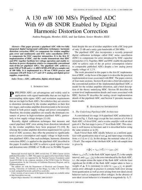
A 130 mW 100 MS/s Pipelined ADC With 69 dB SNDR Enabled by ...
A 130 mW 100 MS/s Pipelined ADC With 69 dB SNDR Enabled by ...
A 130 mW 100 MS/s Pipelined ADC With 69 dB SNDR Enabled by ...

You also want an ePaper? Increase the reach of your titles
YUMPU automatically turns print PDFs into web optimized ePapers that Google loves.
3314 IEEE JOURNAL OF SOLID-STATE CIRCUITS, VOL. 44, NO. 12, DECEMBER 2009<br />
A <strong>130</strong> <strong>mW</strong> <strong>100</strong> <strong>MS</strong>/s <strong>Pipelined</strong> <strong>ADC</strong><br />
<strong>With</strong> <strong>69</strong> <strong>dB</strong> <strong>SNDR</strong> <strong>Enabled</strong> <strong>by</strong> Digital<br />
Harmonic Distortion Correction<br />
Andrea Panigada, Member, IEEE, and Ian Galton, Senior Member, IEEE<br />
Abstract—This paper presents a pipelined <strong>ADC</strong> with two fully<br />
integrated digital background calibration techniques: harmonic<br />
distortion correction (HDC) to compensate for residue amplifier<br />
gain error and nonlinearity and DAC noise cancellation (DNC)<br />
to compensate for DAC capacitor mismatches. It is the first IC<br />
implementation of HDC, and the results demonstrate that HDC<br />
and DNC together facilitate low-voltage operation and enable reductions<br />
in power dissipation relative to comparable conventional<br />
state-of-the-art pipelined <strong>ADC</strong>s. The pipelined <strong>ADC</strong> achieves a<br />
peak SNR of 70 <strong>dB</strong> and a I <strong>dB</strong>FS SFDR of 85 <strong>dB</strong> at a sample-rate<br />
of <strong>100</strong> MHz. It is implemented in a 90 nm CMOS process and<br />
consumes <strong>130</strong> <strong>mW</strong> from 1.2 V and 1.0 V analog and digital power<br />
supplies, respectively.<br />
Index Terms—<strong>ADC</strong>, calibration, digital, mixed signal.<br />
I. INTRODUCTION<br />
P<br />
IPELINED <strong>ADC</strong>s are advantageous and widely used in<br />
applications with signal bandwidths that are too high for<br />
oversampling delta-sigma <strong>ADC</strong>s and resolution requirements<br />
that are too high for flash <strong>ADC</strong>s. Nevertheless they are sensitive<br />
to distortion introduced <strong>by</strong> the residue amplifiers in their first<br />
few stages, and residue amplifier distortion tends to be inversely<br />
related to both power supply voltage and power consumption.<br />
Therefore, the residue amplifiers are usually the dominant consumers<br />
of power in high-resolution pipelined <strong>ADC</strong>s, particularly<br />
in low supply voltage designs [1]–[6].<br />
Recently, digital calibration techniques that measure and<br />
cancel pipelined <strong>ADC</strong> error arising from distortion introduced<br />
<strong>by</strong> the residue amplifiers have been proposed [7]–[10]. By<br />
relaxing the residue amplifier distortion requirement for a given<br />
level of <strong>ADC</strong> accuracy, they offer the potential to significantly<br />
reduce power consumption and supply voltage in high-resolution<br />
pipelined <strong>ADC</strong>s. One such technique, harmonic distortion<br />
correction (HDC), is applied to the pipelined <strong>ADC</strong> described in<br />
this paper. It enables the <strong>ADC</strong> to achieve a peak signal to noise<br />
and distortion ratio (<strong>SNDR</strong>) of 70 <strong>dB</strong> over its 50 MHz Nyquist<br />
Manuscript received April 26, 2009; revised July 27, 2009. Current version<br />
published December 11, 2009. This paper was approved <strong>by</strong> Guest Editor Vadim<br />
Gutnik. This work was supported <strong>by</strong> the National Science Foundation under<br />
Award 0515286, <strong>by</strong> the corporate members of the UCSD Center for Wireless<br />
Communications, <strong>by</strong> the University of California Discovery Program, and <strong>by</strong><br />
STMicroelectronics.<br />
The authors are with the Department of Electrical and Computer Engineering,<br />
University of California at San Diego, La Jolla, CA 92093 USA<br />
(e-mail: panigada@ucsd.edu; galton@ece.ucsd.edu).<br />
Color versions of one or more of the figures in this paper are available online<br />
at http://ieeexplore.ieee.org.<br />
Digital Object Identifier 10.1109/JSSC.2009.2032637<br />
0018-9200/$26.00 © 2009 IEEE<br />
band despite the use of residue amplifiers with a DC loop gain<br />
of only 23 <strong>dB</strong> and a unity gain bandwidth of 200 MHz.<br />
The pipelined <strong>ADC</strong> also incorporates a recently proposed<br />
digital calibration technique called DAC noise cancellation<br />
(DNC) to compensate for error introduced <strong>by</strong> DAC capacitor<br />
mismatches [11]. Together, HDC and DNC enable the pipelined<br />
<strong>ADC</strong> to achieve state of the art power consumption relative<br />
to comparable published <strong>ADC</strong>s despite a low analog power<br />
supply voltage of 1.2 V.<br />
The work presented in this paper is the first IC implementation<br />
of HDC, so the focus of the paper is to describe the practical<br />
implementation issues associated with HDC. The paper consists<br />
of four main sections. Section II provides a brief description of<br />
the conventional portion of the implemented pipelined <strong>ADC</strong>, a<br />
model for the residue amplifier distortion, and a brief description<br />
of the theory underlying HDC. Section III describes the<br />
system-level implementation details and issues associated with<br />
HDC, Section IV describes the analog circuit implementation<br />
details of the pipelined <strong>ADC</strong>, and Section V presents measurement<br />
results.<br />
II. BACKGROUND INFORMATION<br />
A. The Underlying <strong>Pipelined</strong> <strong>ADC</strong> Architecture<br />
A conventional six-stage 14-b pipelined <strong>ADC</strong> architecture is<br />
shown in Fig. 1. Each stage except the last consists of a 9-level<br />
flash <strong>ADC</strong>, a 9-level DAC, and a residue amplifier with an ideal<br />
gain of 4. The last stage is just a 17-level flash <strong>ADC</strong>. This structure<br />
is well known in literature and it is described below using<br />
the same notation as in [8].<br />
Each 9-level flash <strong>ADC</strong> ideally behaves as a uniform quantizer<br />
with quantization step of size and input range extending<br />
from to . In this design, the nominal value of is<br />
170 mV. The output of the th flash <strong>ADC</strong> at the th sample time<br />
is given <strong>by</strong><br />
where is the flash <strong>ADC</strong> input signal, is the sample<br />
interval, and is the error introduced <strong>by</strong> the flash <strong>ADC</strong>,<br />
i.e., the output minus the input of the flash <strong>ADC</strong> with the least<br />
significant bit (LSB) of the flash <strong>ADC</strong> output taken to have a<br />
weight of . It is customary to refer to as quantization<br />
error although in practice it contains both error arising<br />
from quantization as well as error arising from non-ideal circuit<br />
behavior such as comparator offset voltages. In the absence of<br />
non-ideal circuit behavior it is bounded in magnitude <strong>by</strong> .<br />
(1)
PANIGADA AND GALTON: PIPELINED <strong>ADC</strong> WITH <strong>69</strong> <strong>dB</strong> <strong>SNDR</strong> ENABLED BY DIGITAL HARMONIC DISTORTION CORRECTION 3315<br />
Fig. 1. Block diagram of a 14-b pipelined <strong>ADC</strong>.<br />
The 9-level DAC converts the output of the flash <strong>ADC</strong> into<br />
analog format. The difference between the pipelined <strong>ADC</strong> input<br />
sample and the output of the DAC, called the residue, is amplified<br />
<strong>by</strong> the residue amplifier and the result is fed to the next<br />
pipeline stage.<br />
It follows from (1) that in the absence of non-ideal circuit<br />
behavior, the input to and output of the th residue amplifier at<br />
the th sample time are<br />
and<br />
respectively. In this case the output of the<br />
(2)<br />
th residue amplifier<br />
is bounded between and , whereas the input range of<br />
the subsequent stage to which it is applied extends from<br />
to . The extra input range is called over range margin. Its<br />
purpose is to accommodate error from non-ideal circuit behavior<br />
such as flash <strong>ADC</strong> threshold deviations.<br />
As indicated in Fig. 2, the output of the divide-<strong>by</strong>-four block<br />
in the th pipeline stage, referred to as the stage’s digitized<br />
residue, can be written as .<br />
Therefore, it follows from (1) and (2) that the output of the<br />
stage can be written as<br />
th<br />
where , and . Recursive application of<br />
(1) and (2) in (3) gives<br />
This implies that for each , stages through 6 together behave<br />
as a (16–2 k)-b <strong>ADC</strong>. For example, stages 2 through 6 together<br />
behave as a 12-b <strong>ADC</strong>.<br />
B. The Residue Amplifier Distortion Problem<br />
The residue amplifier is usually implemented as an op-amp<br />
in a switched capacitor feedback loop [1]–[6], [10], [12], [17],<br />
(3)<br />
(4)<br />
Fig. 2. Pipeline stages and CI.<br />
[20], [24], [25]. When op-amp hard nonlinearities caused <strong>by</strong> effects<br />
like slew rate limiting or clipping are negligible, the residue<br />
amplifier tends to be well modeled as a memoryless, weakly<br />
nonlinear function of the amplifier’s input voltage, as shown in<br />
Fig. 3, with<br />
where is a linear gain error coefficient and for are<br />
nonlinear distortion coefficients.<br />
Fig. 4 shows a simplified representation of the pipelined <strong>ADC</strong><br />
that includes the effect of op-amp nonlinearity in the first stage.<br />
Applying the same reasoning used above to obtain (4), it follows<br />
that<br />
(5)<br />
(6)
3316 IEEE JOURNAL OF SOLID-STATE CIRCUITS, VOL. 44, NO. 12, DECEMBER 2009<br />
Fig. 3. Model of the residue amplifier with distortion.<br />
Fig. 4. Simplified representation of the 14-b pipelined <strong>ADC</strong> including distortion<br />
from the residue amplifier.<br />
where in the last expression has been replaced <strong>by</strong><br />
(4) with . Therefore, the term appears in the<br />
output of the pipelined <strong>ADC</strong>. Furthermore, it follows from (2)<br />
that the term is a function of the quantization noise<br />
from the flash <strong>ADC</strong> in Stage 1 which is a nonlinear function of<br />
the input signal.<br />
The conventional way to address this problem is to rely on<br />
feedback to suppress the residue amplifier distortion: the higher<br />
the gain and bandwidth of the op-amp, the better the suppression.<br />
Therefore, in a conventional pipelined <strong>ADC</strong> design, the<br />
magnitudes of the coefficients in are reduced to the point<br />
that has negligible effect on the digital output signal. Unfortunately,<br />
this is usually done at the expense of increased power<br />
consumption and circuit area.<br />
C. HDC Overview<br />
The alternative approach taken in this design is to use<br />
op-amps with larger magnitudes of the coefficients in ,in<br />
return for lower op-amp power and area consumption, and then<br />
digitally estimate and cancel the resulting nonlinear distortion<br />
in the pipelined <strong>ADC</strong> output via HDC.<br />
Fig. 5. Correction of the distortion in the digitized residue.<br />
As described in Section IV, the op-amp used in this design has<br />
an open loop DC gain of 43 <strong>dB</strong> which translates into a residue<br />
amplifier DC loop gain of 23 <strong>dB</strong>. Transistor level simulations<br />
under typical conditions indicate that the residue amplifier is<br />
well-modeled as shown in Fig. 3 with , ,<br />
, and for . <strong>With</strong>out<br />
HDC, the resulting <strong>dB</strong>FS signal-to-noise and distortion ratio<br />
(<strong>SNDR</strong>) for the pipelined <strong>ADC</strong> would be 43 <strong>dB</strong>, which is 26 <strong>dB</strong><br />
below the target specification.<br />
Extensive circuit simulations run during the design phase<br />
of the pipelined <strong>ADC</strong> IC further indicate that only the distortion<br />
introduced <strong>by</strong> and must be corrected to achieve<br />
the 70 <strong>dB</strong> <strong>SNDR</strong> target specification. The magnitudes of<br />
for even values of are negligible because of the differential<br />
circuitry used throughout the <strong>ADC</strong>, and magnitudes of for<br />
odd values of are negligible because hard nonlinearities<br />
such as slew rate limiting in the op-amps are small. Therefore,<br />
HDC is configured in this work to compensate only for residue<br />
amplifier distortion associated with and .<br />
A full description of the theory behind HDC is presented in<br />
[8]. The purpose of this section is to provide a brief overview<br />
of HDC with enough information to support the subsequent description<br />
of its application to the pipelined <strong>ADC</strong> prototype.<br />
HDC can be applied to each stage of a pipelined <strong>ADC</strong> to<br />
compensate for the distortion introduced <strong>by</strong> that stage’s residue<br />
amplifier. In each stage it consists of an estimation portion and<br />
a correction portion. The former estimates the coefficients<br />
in (5) for that stage’s residue amplifier, and the latter uses the<br />
estimates to compensate for the distortion. In the following, the<br />
correction portion is described prior to the estimation portion,<br />
both in the context of HDC applied to the first pipeline stage.<br />
1) Correction Portion of HDC: Neglecting the quantization<br />
error and assuming ideal behavior of the stages 2–6,<br />
can be expressed as<br />
Fig. 5 shows the proposed correction method, which<br />
implements:<br />
(7)<br />
terms with fifth and higher order (8)
PANIGADA AND GALTON: PIPELINED <strong>ADC</strong> WITH <strong>69</strong> <strong>dB</strong> <strong>SNDR</strong> ENABLED BY DIGITAL HARMONIC DISTORTION CORRECTION 3317<br />
As detailed in [8], the correction process introduces fifth and<br />
higher order distortion terms in , but they can be<br />
neglected because the power of the error they introduce in the<br />
pipelined <strong>ADC</strong> output is much lower than the target noise floor.<br />
2) Estimation Portion of HDC: A digital calibration sequence,<br />
, is added to the output of the flash <strong>ADC</strong> as shown<br />
in Fig. 6 to enable estimation of the and coefficients<br />
associated with the residue amplifier in the first pipeline stage.<br />
As indicated in the figure, is converted to analog form<br />
<strong>by</strong> the DAC, so it is subtracted from the input of the residue<br />
amplifier. This causes several extra terms related to to<br />
appear as components in the digitized residue. Two of the extra<br />
terms are proportional to and , and the HDC<br />
estimation algorithm uses these terms to estimate the and<br />
coefficients.<br />
HDC is a background calibration technique so it must estimate<br />
the and coefficients during normal operation of the<br />
<strong>ADC</strong>. Therefore, must be such that the terms proportional<br />
to and can be measured in the digital residue<br />
even in the presence of other, potentially much larger and unknown<br />
terms related to the pipelined <strong>ADC</strong> input signal. Furthermore,<br />
it must have a relatively small magnitude so it only<br />
occupies a portion of the over range margin of the subsequent<br />
pipeline stage.<br />
The simplest known calibration sequence with these properties<br />
is a four-level sequence of the form<br />
, where the three sequences are 2-level, independent,<br />
zero-mean pseudo-random sequences that take on values of<br />
(in this design ). For example, with this calibration<br />
sequence the term in the digitized residue contains<br />
the term . Since is a known,<br />
2-level, zero-mean pseudorandom sequence that takes on values<br />
of and is uncorrelated with all the other signal components<br />
in the digitized residue, it follows that the average of the product<br />
of the digitized residue and converges to<br />
regardless of the input signal to the pipelined <strong>ADC</strong>.<br />
The HDC algorithm calculates the following correlations:<br />
where and is the number of samples<br />
averaged (e.g., was used for most of the measurement<br />
results presented in Section V). It can be verified that, provided<br />
the residue amplifier is the only significant source of nonlinearity<br />
in the system, these correlations converge to<br />
(9)<br />
(10)<br />
in the limit as regardless of the input to the pipelined<br />
<strong>ADC</strong>, where indicates the infinite time average operation.<br />
Fig. 6. Simplified representation of a 14-b pipelined <strong>ADC</strong> with HDC applied<br />
to the first pipeline stage.<br />
The HDC algorithm uses these correlation values to calculate<br />
the coefficients required <strong>by</strong> (8) as follows:<br />
(11)<br />
It follows from (10) that is an unbiased estimate of ,<br />
whereas is an estimate of that is biased <strong>by</strong> . Therefore,<br />
accurate estimation of requires knowledge of . Unlike<br />
HDC, the gain error correction (GEC) technique presented<br />
in [12] calculates the equivalent of and uses it as an estimate<br />
of directly, so it implicitly assumes that is negligible. Consequently,<br />
highly linear residue amplification is a prerequisite<br />
for GEC to function properly.<br />
Simulation results under the typical conditions described in<br />
Section II-B indicate that if the HDC correction is performed as<br />
indicated in Fig. 5 except with set to zero, then the <strong>SNDR</strong><br />
and SFDR decrease <strong>by</strong> 1.7 <strong>dB</strong> and 3 <strong>dB</strong>, respectively. However,<br />
if HDC correction is performed as indicated in Fig. 5 except<br />
with set to zero in (11), which is equivalent to the correction<br />
performed <strong>by</strong> GEC, then the <strong>SNDR</strong> and SFDR drop <strong>by</strong> about<br />
7 <strong>dB</strong> and 13 <strong>dB</strong>, respectively.<br />
III. DIGITAL CALIBRATION SYSTEM-LEVEL DETAILS<br />
A. Required Analog Enhancements for HDC<br />
Most of the enhancements required to implement HDC in a<br />
pipelined <strong>ADC</strong> stage are digital. The only exception is that the<br />
DAC must be modified as described in this section. To simplify<br />
the notation, the description is in the context of HDC applied to<br />
first stage.<br />
The calibration signal, , described above takes on<br />
values of , , , and and the output<br />
of the flash <strong>ADC</strong>, , takes on values of , ,
3318 IEEE JOURNAL OF SOLID-STATE CIRCUITS, VOL. 44, NO. 12, DECEMBER 2009<br />
, and , so a <strong>69</strong>-level DAC with step size of<br />
is required to represent the signal . Although<br />
a <strong>69</strong>-level DAC could be implemented, as explained later it is<br />
more convenient to implement a 65-level DAC. Therefore, a<br />
65-level DAC has been implemented in this design. To ensure<br />
that stays within the 65 level range of the DAC,<br />
the addition of is disabled when , i.e., when<br />
the input to the flash <strong>ADC</strong> has a magnitude between and<br />
. 1<br />
A 65-level DAC can be implemented <strong>by</strong> adding the outputs<br />
of 64 unity-weighted 1-b DACs. In absence of mismatches<br />
among the 1-b DACs, the output of the DAC would be<br />
. Unfortunately, mismatches among the 1-b<br />
DACs inevitably introduced during fabrication cause the output<br />
of the DAC to be<br />
(12)<br />
where is a constant gain, is a constant offset, and<br />
is non-constant error referred to as DAC noise [11]. If<br />
each possible value of is mapped to a unique set of<br />
input bits to the 64 1-b DACs, then is a deterministic<br />
nonlinear function of the flash <strong>ADC</strong> output signal, in which case<br />
the DAC is a source of nonlinear distortion.<br />
Dynamic element matching (DEM) is used in this design to<br />
eliminate the DAC as a significant source of nonlinear distortion.<br />
The idea behind DEM is that for most values of<br />
, there are multiple ways to set the input bits of the 1-b DACs<br />
that would yield in the absence of mismatches<br />
among the 1-b DACs. A DEM encoder prior to the 1-b<br />
DACs pseudo-randomly selects one of these valid sets of input<br />
bits each sample period, in such a way that has zero<br />
mean and is uncorrelated with .<br />
In a pipeline stage, the propagation delay between the output<br />
of the Flash <strong>ADC</strong> and the output of the DEM encoder must be<br />
minimized, because it reduces the time available for the sampling<br />
phase or the amplification phase of the stage. Reducing the<br />
time for the sampling phase reduces the pipelined <strong>ADC</strong>’s input<br />
signal bandwidth, whereas reducing the time for the amplification<br />
phase reduces the settling time available for the op-amp.<br />
In this implementation, the time allocated for the propagation<br />
delay is about 300 ps.<br />
One way to achieve this target propagation delay is to use two<br />
layers of parallel transmission gates (T-gates). The first layer of<br />
4 T-gates would compute the sum and ,<br />
and the second layer of T-gates would implement<br />
the DEM encoder. Unfortunately this solution requires 4352<br />
T-gates with an estimated area of 60,000 m not including the<br />
overhead due to routing. Therefore, this strategy was considered<br />
impractical.<br />
Instead the segmented DEM DAC shown in Fig. 7 has been<br />
implemented. The structure has 14 1-b DACs, 8 with weight<br />
with weight with weight and with weight<br />
1 Disabling the addition of ‘“ may also slow down the convergence of the<br />
HDC algorithm, because the samples for which ‘“ is disabled are not used in<br />
the correlation processes described <strong>by</strong> (9). For example, a sinusoid with a fullscale<br />
amplitude of RXS1 would cause the addition of ‘“ to be disabled 43% of<br />
the time. No reduction in convergence time occurs for signals with magnitudes<br />
below QXS1.<br />
Fig. 7. Simplified block diagram of the implemented segmented DEM DAC.<br />
. As quantified below, the benefit of this structure is that<br />
the DEM encoder can be implemented with much lower circuit<br />
area than the DEM encoder mentioned above. However,<br />
as explained in [13], a fundamental limitation of segmented<br />
DEM DACs is that to achieve the desired properties<br />
they must limit the range of their input sequences to less than<br />
the total possible output range of their 1-b DACs. In this case,<br />
the input bits of the 1-b DACs shown in Fig. 7 could be set<br />
to achieve any of 79 output levels, but the DEM encoder is<br />
only able to achieve the desired properties if it limits<br />
the range of the DAC to 65 levels. Therefore, the segmented<br />
DEM DAC requires 22% more capacitance in its set of 1-b<br />
DACs than would be required in a comparable DEM DAC with<br />
64 unity-weighted 1-b DACs. Furthermore, the extra capacitance<br />
introduces a 0.5 <strong>dB</strong> increase in noise. Nevertheless,<br />
these drawbacks are considered worthwhile tradeoffs for<br />
the reduction in DEM encoder complexity.<br />
The signal processing performed <strong>by</strong> the DEM encoder is that<br />
of the segmented tree-structured DEM encoder shown in Fig. 8<br />
with an input sequence given <strong>by</strong> 2<br />
(13)<br />
The DEM encoder is similar to that presented in [13], [14] 3<br />
. It consists of 13 digital switching blocks. Switching blocks<br />
, , and , are called segmenting switching blocks<br />
and the remaining switching blocks are called non-segmenting<br />
switching blocks. Each switching block calculates its two output<br />
sequences as a function of its input sequence and one of 13<br />
pseudo-random 1-b sequences, , , , and<br />
, , and 7. The sequences are designed to<br />
2The use of notation ‘“ for the DEM encoder signals has been chosen<br />
to align with [13], [14] ( ‘“ should not be confused with the calibration<br />
sequence ‘“).<br />
3A <strong>69</strong>-level version of the DEM DAC could have been implemented <strong>by</strong> combining<br />
the techniques presented in [13] and [15], but it would have been more<br />
complex.
PANIGADA AND GALTON: PIPELINED <strong>ADC</strong> WITH <strong>69</strong> <strong>dB</strong> <strong>SNDR</strong> ENABLED BY DIGITAL HARMONIC DISTORTION CORRECTION 3319<br />
Fig. 8. 65-level segmented DAC with DEM encoder.<br />
Fig. 9. The three configurations of the first layer of T-gates (only ON switches<br />
are shown).<br />
well-approximate white random sequences that are independent<br />
from each other and , and each take on values of 0 and 1<br />
with equal probability. The switching blocks function as shown<br />
in Fig. 8 with<br />
for , 5, and 6, and<br />
if<br />
if<br />
if .<br />
if<br />
if<br />
if .<br />
for , 2, and 3, and , and .<br />
(14)<br />
(15)<br />
Fig. 10. Implementation of the DEM encoder and ‘“ adder.<br />
In this design, the addition of and and the functionality<br />
of the segmented DEM encoder described above are implemented<br />
such that all time-critical operations are performed <strong>by</strong><br />
a layer of 24 parallel T-gates followed <strong>by</strong> a layer of 64 parallel<br />
T-gates. Therefore, the total propagation time is equal to that of<br />
2 cascaded T-gates. The way this is achieved is explained below.
3320 IEEE JOURNAL OF SOLID-STATE CIRCUITS, VOL. 44, NO. 12, DECEMBER 2009<br />
Fig. 11. Block diagram of the HDC logic in the first pipeline stage.<br />
Note from (13) and (14) that the amplitude of is<br />
chosen depending upon the parity of , which in turn<br />
depends only on . Therefore, the calculations performed<br />
<strong>by</strong> switching block do not involve the output of the flash<br />
<strong>ADC</strong>, , so they can be performed before is available.<br />
Similar reasoning applies to switching blocks , , ,<br />
, and . Therefore, the input bits to the bottom 6 1-b<br />
DACs in Fig. 8 can be computed before the Flash <strong>ADC</strong> output<br />
is available.<br />
By similar reasoning it can be verified that the upper output<br />
of is<br />
(16)<br />
where is a function of , , , and ,<br />
and can take on values of only , 0, and 1. A low-latency<br />
implementation of (16) is achieved <strong>by</strong> combining 24 parallel<br />
T-gates that can implement the three input-output connection<br />
configurations shown in Fig. 9. In this design can<br />
take on values of 0, 1, , and 8 and is provided <strong>by</strong> the flash<br />
<strong>ADC</strong> in the form of a thermometer code. Therefore, the mapping<br />
shown in Fig. 9 results in a thermometer code representation of<br />
. Since is known before the flash <strong>ADC</strong><br />
output is ready, the T-gate configuration is selected in advance,<br />
there<strong>by</strong> minimizing latency.<br />
Fig. 10 shows the implementation of the combined<br />
summer and the segmented DEM encoder. The first<br />
layer of 24 T-gates implements (16) as described above, and<br />
the second layer of 64 T-gates maps the combined operation of<br />
, , , , , , . As demonstrated in [11]<br />
and [12] the configuration of such T-gates does not depend on<br />
the signal , so it is selected in advance. Standard logic<br />
is used to realize all components for which the timing is not<br />
critical. These components include the pseudo-random number<br />
generator (PRNG), switching blocks , , , ,<br />
, and , and all the circuitry that drives the T-gates.<br />
As described above, when the addition of<br />
must be disabled. To do this with minimal latency, the inputs to<br />
the bottom six 1-b DACs in Fig. 7 are computed for both cases<br />
(addition of enabled and disabled) and then the correct<br />
choice is selected <strong>by</strong> a multiplexer. For the upper 8 1-b DACs,<br />
the T-gates in the first layer provide the disabling function: it<br />
can be verified from Fig. 9 that when the flash <strong>ADC</strong> output is<br />
full scale (all the thermometer bits are 1’s or 0’s), has no<br />
effect on the signal.<br />
B. HDC Digital Logic<br />
The details of the HDC block in Fig. 6 are shown in Fig. 11.<br />
The HDC block implements the calculations described in<br />
Section II-C with some extra features to reduce complexity.<br />
The signal is requantized to 6 bits prior to the correlators,<br />
and its squared value is requantized to 4 bits prior to<br />
the average and dump operation to reduce the size of the<br />
HDC logic. Dithered requantizers are used to ensure that the<br />
resulting quantization noise is zero-mean and uncorrelated with<br />
[16], which is sufficient to avoid corrupting the correlations.<br />
Although the quantization noise slows down the correlation<br />
process slightly, it has been found from simulation and<br />
approximate analysis that the increase in convergence time is<br />
negligible.<br />
The average and dump blocks shown in Fig. 11 compute<br />
, and according to (10). They each average<br />
valid samples (i.e., samples for which was enabled) where<br />
is an integer between 28 and 34 (selectable via serial port<br />
control), and then output the average. Each time a new average<br />
is produced, the average and dump blocks are reset and start<br />
over. When new averages are ready, they are scaled as necessary<br />
to obtain , and , and further processed <strong>by</strong> digital<br />
logic that implements (11). Since the estimates are updated only<br />
once every valid samples, all the post processing only needs<br />
to produce new values at the same low rate, thus allowing a<br />
low-power and low-area realization. Four full speed multipliers<br />
and one adder implement (8).<br />
C. Application of HDC and DNC to Multiple Pipeline Stages<br />
In this design, HDC has been applied to the first three stages,<br />
as shown in Fig. 12. The calibration sequences , and<br />
are added and three HDC blocks, labeled HDC1, HDC2,<br />
and HDC3, are included in the first three stages, respectively.<br />
As explained in Section III-D, the coefficient estimation process
PANIGADA AND GALTON: PIPELINED <strong>ADC</strong> WITH <strong>69</strong> <strong>dB</strong> <strong>SNDR</strong> ENABLED BY DIGITAL HARMONIC DISTORTION CORRECTION 3321<br />
Fig. 12. Complete block diagram of the implemented 14-b pipelined <strong>ADC</strong>.<br />
performed <strong>by</strong> HDC in a given stage is most accurate when the<br />
residue amplifier in that stage is the primary source of distortion.<br />
Therefore, the coefficient estimation process is implemented<br />
first in Stage 3, then in Stage 2, and then in Stage 1, at which<br />
point the cycle is repeated.<br />
Fig. 12 also shows blocks that implement DNC in the first<br />
three pipeline stages. Each DNC block estimates and cancels the<br />
DAC noise introduced <strong>by</strong> the corresponding 65-level DAC. The<br />
implementation of DNC has been explained in [12], so further<br />
description of it is omitted from this paper.<br />
HDC and DNC operate in the background during normal operation<br />
of the pipelined <strong>ADC</strong>, so they adapt to environmental<br />
changes without interrupting normal <strong>ADC</strong> operation. The convergence<br />
time is approximately 129 seconds (43 seconds per<br />
stage, limited <strong>by</strong> HDC convergence), so the DNC and HDC coefficients<br />
are updated every 129 seconds.<br />
Therefore, the <strong>ADC</strong> does not operate at full accuracy for the<br />
first 129 seconds of operation. Although not implemented, a<br />
foreground calibration mode to address this issue can be implemented<br />
with no changes to HDC or DNC except for zeroing the<br />
input signal and using in place of in each of the first<br />
three stages. While the <strong>ADC</strong> would not perform analog-to-digital<br />
conversion of the input signal while the foreground calibration<br />
mode is converging, the convergence is much faster than<br />
that of the normal background calibration mode. Simulations<br />
indicate that the foreground calibration mode would reduce the<br />
initial convergence time to less than a second. Thus, it would facilitate<br />
fast calibration at start-up, or after a long stand-<strong>by</strong> time,<br />
depending on the application. Once the <strong>ADC</strong> is calibrated the<br />
first time, HDC would continue to operate in the background to<br />
track environmental changes as described above.<br />
D. Effect of Quantizer Nonlinearity On HDC<br />
The estimation portion of HDC in a given pipeline stage measures<br />
distortion in that stage’s digitized residue regardless of<br />
its source, but the correction portion of HDC is based on the<br />
assumption that all of the measured distortion came from that<br />
stage’s residue amplifier. Therefore, the theory behind HDC implicitly<br />
assumes that the residue amplifier is the only significant<br />
source of nonlinearity in the pipelined <strong>ADC</strong>.<br />
Nevertheless, under certain conditions the flash <strong>ADC</strong>s can be<br />
a significant source of nonlinearity in a pipelined <strong>ADC</strong>. Ideally,<br />
only the last stage’s flash <strong>ADC</strong> quantization noise, i.e.,<br />
, appears in the output of the pipelined <strong>ADC</strong> and the<br />
thermal noise level is high enough that it acts like dither and<br />
prevents from introducing significant nonlinear distortion.<br />
However, due to non-zero and , the quantization<br />
error from the first 5 stages is not perfectly canceled in practice,<br />
and this causes leakage of quantization error to the output. Even<br />
in the stages with HDC some leakage of quantization error always<br />
occurs, because the estimation process is never perfect.<br />
To simplify the description of the problem, suppose the<br />
pipelined <strong>ADC</strong> has ideal components except that the residue<br />
amplifier in the second stage has a non-zero value of such<br />
that a fraction, , of quantization error, , leaks into<br />
the digitized residue, . In this case it follows from (10)<br />
that and of HDC1 contain terms<br />
and , respectively. If either of<br />
these terms are non-zero, the estimates of the parameters<br />
and in stage 1 are corrupted. For example, it can be shown<br />
that when the pipelined <strong>ADC</strong> input stays in the range<br />
to , , whereas when<br />
the pipelined <strong>ADC</strong> input stays in the range to ,<br />
. In both cases even a<br />
small leakage of causes the estimate of to<br />
have a magnitude of (recall that for this<br />
hypothetical example). Thus, the estimation error is almost<br />
50% of the typical value of achieved <strong>by</strong> the<br />
op-amps used in the pipelined <strong>ADC</strong> prototype IC.<br />
More generally, for DC and low-amplitude pipelined<br />
<strong>ADC</strong> input signals the correlation between and<br />
tends to be nonzero, which corrupts the estimates<br />
of . This problem is negligible when the input signal<br />
amplitude is greater than <strong>dB</strong>FS, because in such cases the<br />
signal at the input of the second stage’s flash <strong>ADC</strong> is sufficiently<br />
busy that is close to zero.<br />
The problem described above is not unique to HDC. It affects<br />
all of the known residue amplifier distortion calibration techniques<br />
because they each use a pipelined <strong>ADC</strong> to measure the<br />
distortion from its own residue amplifiers. In each case, the distortion<br />
from all sources in the pipelined <strong>ADC</strong> is measured but
3322 IEEE JOURNAL OF SOLID-STATE CIRCUITS, VOL. 44, NO. 12, DECEMBER 2009<br />
the distortion is corrected under the assumption that the residue<br />
amplifiers are the only significant distortion sources.<br />
E. An Improved Calibration Sequence<br />
One way to mitigate the problem is to use a calibration sequence<br />
consisting of 5 sequences instead of 3 sequences,<br />
i.e., . The<br />
2 extra sequences add enough dither to decorrelate<br />
from and , thus allowing successful convergence<br />
even for low-amplitude pipelined <strong>ADC</strong> input signals.<br />
A drawback of this solution is that the two extra sequences<br />
increase the magnitude of the calibration sequence <strong>by</strong><br />
, so additional over range margin is used <strong>by</strong> the terms in<br />
the residue amplifier output associated with the calibration sequence.<br />
In this design, the drawback was found to be acceptable<br />
because the extra area and power consumption required to correspondingly<br />
reduce the flash <strong>ADC</strong> threshold errors, negligibly<br />
increased the overall circuit area and power consumption of the<br />
pipelined <strong>ADC</strong> prototype IC.<br />
Unfortunately, a wiring mistake was made in the pipelined<br />
<strong>ADC</strong> prototype IC which caused the HDC calibration sequence<br />
in each HDC-enabled pipeline stage to be the sum of three rather<br />
than five sequences. All five sequences are generated on<br />
chip for each HDC-enabled pipeline stage, but the wiring mistake<br />
prevented two of the five sequences from being used. As<br />
described above, the consequence of this mistake is that each<br />
stage’s estimates of the and coefficients tend to be wrong<br />
for small-amplitude pipelined <strong>ADC</strong> input signals.<br />
Normally, each HDC block continually updates its coefficients,<br />
but it can optionally freeze the coefficients after<br />
convergence. In order to test the pipelined <strong>ADC</strong> for small-amplitude<br />
input signals, the measurement results presented in<br />
Section V were obtained <strong>by</strong> allowing the HDC blocks to<br />
converge with a large-amplitude pipelined <strong>ADC</strong> input signal<br />
and then freezing the coefficients via serial port control. Measurements<br />
with frozen coefficients for numerous input signals,<br />
including small input signals, indicate that full performance is<br />
achieved in all cases as expected.<br />
F. A Detection Method for Invalid Correlations<br />
It can be shown that the dithering effect provided <strong>by</strong><br />
adding the five sequences completely removes any<br />
correlation between and the sequences and<br />
, in the case where . When ,<br />
there are some small ranges of pipelined <strong>ADC</strong> input signals<br />
for which the quantization error is still correlated<br />
with . For example, suppose .<br />
Then a pipelined <strong>ADC</strong> input signal that stays between<br />
and causes ,<br />
and one that stays between and causes<br />
, both of which would<br />
lead to invalid estimates of the distortion parameters.<br />
As seen in the above example, the ranges of inputs for which<br />
come in doublets, and each side<br />
of the doublet has opposite correlations. Therefore, input signals<br />
that are sufficiently busy spend roughly equal time in each of<br />
the two sides of the doublet, so the effect of this undesired correlation<br />
tends to be small. Consequently the existence of these<br />
doublets does not seem to affect HDC accuracy significantly.<br />
However, if necessary it is possible to detect invalid correlation<br />
results so as to avoid updating the distortion coefficients,<br />
until a new successful estimate is available. In the remainder of<br />
this section, a method to detect a bad estimate is described 4.<br />
The output of the Flash <strong>ADC</strong> of stage 2 can be correlated<br />
against and the result can be used with the<br />
output of the second correlator of HDC1 to generate an estimate<br />
of the quantity<br />
It follows from the reasoning described in Section II that<br />
and<br />
(17)<br />
(18)<br />
(19)<br />
where the last term in (19) is due to the leakage of quantization<br />
error. In practice and<br />
. Therefore, whenever the magnitude of the estimate of<br />
(17) is larger than , where is an upper<br />
bound on it indicates that is large<br />
enough to cause the HDC estimates to be corrupted. Furthermore,<br />
need not be a tight upper bound on . For example,<br />
in this system setting would work because<br />
it would ensure that the estimate of is precise within<br />
10% assuming and , which is<br />
sufficient accuracy to achieve the target <strong>ADC</strong> performance.<br />
IV. ANALOG CIRCUIT DETAILS<br />
Additional details of the analog and mixed-signal portions of<br />
the first three pipeline stages are shown in Fig. 13(a). The fourth<br />
and fifth stages have a similar structure, except no calibration<br />
sequence is added, and therefore a 9-level DEM DAC with a step<br />
size of is used in place of the 65-level DEM DAC. Additional<br />
details of the last pipeline stage are shown in Fig. 13(b).<br />
As shown in Fig. 13(a) the continuous time input signal is<br />
sampled <strong>by</strong> two separate passive sampling networks, the outputs<br />
of which are connected to the residue amplifier and the flash<br />
<strong>ADC</strong>, respectively [17]. The DAC is realized as a separate circuit<br />
connected to the input terminals of the residue amplifier.<br />
A differential switched capacitor unit sampling cell with a<br />
simplified timing diagram is shown in Fig. 14. The sampling<br />
network of the residue amplifier consists of 8 such unit sampling<br />
4 The authors were not aware of the presence of such doublets until after the<br />
tape out, so the detection method described in this section was not implemented<br />
in the pipelined <strong>ADC</strong> prototype IC.
PANIGADA AND GALTON: PIPELINED <strong>ADC</strong> WITH <strong>69</strong> <strong>dB</strong> <strong>SNDR</strong> ENABLED BY DIGITAL HARMONIC DISTORTION CORRECTION 3323<br />
Fig. 13. Block diagram of the mixed-signal circuitry in (a) the first three pipeline stages, and (b) the last pipeline stage.<br />
Fig. 14. Unit passive sampling network (bootstrap circuit for f1 d switches not<br />
shown).<br />
cells in parallel, whereas each of the 8 comparators of the 9-level<br />
flash <strong>ADC</strong> uses a quarter-size version of a single unit sampling<br />
cell. Both the capacitors and switches are scaled proportionally<br />
such that the two sampling paths have the same nominal time<br />
constant. The switches between the top plates of the capacitors<br />
and inputs of the op-amp provide isolation from the op-amp<br />
during the sampling phase to improve matching between the<br />
two sampling networks as described in [12], and ensure that the<br />
residue amplifier’s coefficients do not depend on the input<br />
signal. Bootstrapped switches of the type presented in [12] are<br />
used for the continuous-time input sampling switches of both<br />
sampling networks to achieve the necessary linearity.<br />
A separate switched capacitor network has been used for the<br />
DAC to prevent signal-dependent loading of the voltage references.<br />
This benefit comes at the expense of a 3 <strong>dB</strong> increase in<br />
noise and a reduced residue amplifier feedback factor<br />
(1/10 versus 1/6) relative to a design in which the DAC and sampling<br />
network share the same capacitors.<br />
The sampling network of each 1-b DAC with weight is<br />
shown in Fig. 15. Scaled versions of the same cell have been<br />
implemented for the 1-b DACs with weights , and<br />
as required to implement the DAC in Fig. 8. The input bit<br />
from the DEM encoder to each 1-b DAC controls the Swap Cell<br />
during . Bootstrapped switches were not used for the DAC<br />
switches.<br />
By design the dominant sources of noise in the pipelined<br />
<strong>ADC</strong> are noise and thermal noise from the op-amps in<br />
the first few stages. The 14-bit pipelined <strong>ADC</strong> architecture en-<br />
Fig. 15. 1-b DAC sampling network (weight 1).<br />
sures that the quantization noise level is 16 <strong>dB</strong> below the targeted<br />
noise floor. The sampling network switch drivers were<br />
designed and verified <strong>by</strong> simulation to introduce noise that is<br />
similarly well below the targeted noise floor. Therefore, the capacitor<br />
sizes were determined and the op-amps were designed<br />
with the goal of meeting the target SNR specification of 70 <strong>dB</strong>.<br />
The residue amplifier is shown in Fig. 16. It is based on a<br />
Miller compensated two-stage op-amp. Open loop op-amps and<br />
pseudo-differential op-amps were considered as possibilities for<br />
this design, but the two-stage op-amp ultimately was chosen<br />
because of its wide output dynamic range, which is particularly<br />
important given the 1.2 V supply voltage.<br />
The simulated DC open-loop gain and unity gain frequency<br />
of the op-amp in the first pipeline stage’s residue amplifier are<br />
43 <strong>dB</strong> and 1.2 GHz, respectively. The corresponding loop gain<br />
of the residue amplifier is 23 <strong>dB</strong> at DC and has a unity gain<br />
frequency of 200 MHz. The current consumption of the op-amp<br />
is 4.8 mA from a 1.2 V supply.<br />
During the amplification phase, , the feedback capacitor<br />
is connected to the op-amp, whereas during the phase<br />
is disconnected from the op-amp and discharged. During<br />
, the op-amp is reset <strong>by</strong> shorting the differential outputs of<br />
both stages to reduce memory effects [18]. Switched capacitor<br />
common mode feedback circuitry (not shown in Fig. 16) controls<br />
the common mode voltage of the output stage <strong>by</strong> adjusting<br />
.
3324 IEEE JOURNAL OF SOLID-STATE CIRCUITS, VOL. 44, NO. 12, DECEMBER 2009<br />
Fig. 16. Residue amplifier switched capacitor network and op-amp.<br />
Fig. 17. Reference voltage generator.<br />
The voltage references and are generated on<br />
chip as shown in Fig. 17. A set of resistors between the power<br />
supply and ground define the desired voltage reference values<br />
(nominally set to 950 mV and 265 mV, respectively), which are<br />
buffered <strong>by</strong> a pseudo-differential voltage follower and decoupled<br />
<strong>by</strong> external capacitors [19]. The main drawback of<br />
this solution is the need for 2 extra pins for external decoupling.<br />
However the large external capacitors provide a low impedance<br />
over a wide frequency range, and this relaxes the performance<br />
requirements of the internal buffers which need only deliver the<br />
average current required <strong>by</strong> the switching load [20]. The total<br />
DC current consumption for the reference generation circuitry<br />
is 4 mA from a 1.2 V supply, including the current through the<br />
reference ladders.<br />
The same reference voltages and are shared <strong>by</strong><br />
all the DACs and flash <strong>ADC</strong>s in the pipelined <strong>ADC</strong>. The reference<br />
ladders that generate the threshold voltages for the flash<br />
Fig. 18. Common mode voltage generators.<br />
<strong>ADC</strong>s are connected between and . In this design,<br />
each flash <strong>ADC</strong> uses a dedicated reference ladder. The common<br />
mode voltages used for the switched capacitor circuits are generated<br />
as shown in Fig. 18.<br />
Latched comparators of the type presented in [21] are used<br />
in the flash <strong>ADC</strong>s. It is a standard latch with preamplifier consisting<br />
of two resistively loaded differential pairs in series.<br />
The phase generator has been designed with the strategy described<br />
in [12]. A dedicated phase is used as a sampling phase of<br />
the first stage only ( in Fig. 14), such that the sampling instant<br />
(falling edge of ) happens before any other switching event<br />
[22]. This reduces the chance of corrupting the sampling process<br />
with disturbances such as from coupling effects. Care was taken<br />
to minimize sampling jitter <strong>by</strong> placing the clock generator close<br />
to the sampling network in the layout and <strong>by</strong> using a minimum<br />
number of inverters. The simulated jitter due to thermal noise of<br />
the sampling network is <strong>100</strong> fs.<br />
To minimize design time the second through fifth pipeline<br />
stages are replicas of the first stage with only minor modifications.<br />
The only changes are that the residue amplifier, sampling<br />
network, and DAC have been scaled <strong>by</strong> 1/2 in stages 2 and 3<br />
and <strong>by</strong> 1/4 in stages 4 and 5, and the op-amp has been scaled <strong>by</strong><br />
1/2 in the stages 3 and 4 and <strong>by</strong> 1/4 in the stage 5. More aggressive<br />
scaling would have reduced power and area consumption<br />
without sacrificing <strong>ADC</strong> accuracy. Power and area consumption<br />
also could have been reduced without sacrificing <strong>ADC</strong> accuracy<br />
if 1.5-b pipeline stages had been used after the first three stages<br />
[23]. However, neither of these design options were taken because<br />
they would have increased design time.<br />
The pipelined <strong>ADC</strong> prototype IC is implemented in 90 nm<br />
CMOS technology with a deep nWell option, MiM capacitors,<br />
and both high and standard threshold voltage transistors. The<br />
circuit is partitioned into four power supply domains: (i) analog,<br />
(ii) clock drivers & DEM, (iii) clock generator, and (iv) digital,<br />
each of which is powered <strong>by</strong> a separate power supply line. The<br />
nominal power supply voltages of the four domains are 1.2 V,<br />
1.2 V, 1.0 V, and 1.0 V, respectively. To minimize coupling from<br />
the substrate, all active components in the analog sections of<br />
the IC are in deep n-wells, the digital core and serial port interface<br />
(which were laid out with an automated place-and-route<br />
tool) are in a single deep n-well, and the capacitors associated
PANIGADA AND GALTON: PIPELINED <strong>ADC</strong> WITH <strong>69</strong> <strong>dB</strong> <strong>SNDR</strong> ENABLED BY DIGITAL HARMONIC DISTORTION CORRECTION 3325<br />
Fig. 19. Die photograph.<br />
with the switched-capacitor portions of the IC were laid out<br />
above n-wells. On-chip decoupling capacitance is used to reduce<br />
power supply bounce. All pads have ESD protection circuitry.<br />
A die photograph is shown in Fig. 19. The IC is 2.15 mm<br />
<strong>by</strong> 3.35 mm and has an active area of 4 mm .<br />
The IC is packaged in a 56-pin QFN package with exposed<br />
die paddle. All grounds are down-bonded to the exposed paddle.<br />
Critical supply pins and the pins that connect the voltage references<br />
to external decoupling capacitors are double-bonded to<br />
reduce inductance.<br />
V. MEASUREMENT RESULTS<br />
Three randomly chosen copies of the pipelined <strong>ADC</strong> prototype<br />
IC have been tested. Each IC was soldered to one of three<br />
identical printed circuit test boards. Measurement results from<br />
the three test boards are reported in this section.<br />
Each test board includes input signal conditioning circuitry,<br />
a <strong>100</strong> MHz low-jitter crystal oscillator and associated clock<br />
conditioning circuitry, voltage regulators, and digital circuitry<br />
to facilitate acquisition of the output data from and serial port<br />
communication with the pipelined <strong>ADC</strong> prototype IC. The<br />
input conditioning circuitry consists of a transformer followed<br />
<strong>by</strong> two passive RC filter stages to convert the single-ended input<br />
signal from an SMA connector to differential form and suppress<br />
out-of-band noise and distortion. The clock conditioning<br />
circuitry uses a transformer to convert the single-ended clock<br />
signal from the <strong>100</strong> MHz oscillator to differential form. The<br />
output swing of the <strong>100</strong> MHz oscillator is 3.3 V, so high-speed<br />
diodes are connected across the secondary terminals of the<br />
transformer to limit the amplitude of the differential clock<br />
signal to less than 1 V. Four voltage regulators provide the<br />
four power supplies of the pipelined <strong>ADC</strong> prototype IC. Five<br />
other voltage regulators provide power supplies for the other<br />
components on the test board.<br />
Measurements were performed with a variety of single-tone<br />
and two-tone input signals. For each single-tone measurement,<br />
the output of a high-quality sinusoidal laboratory signal source<br />
was passed through a custom-made passive bandpass filter with<br />
a narrow bandwidth centered near the signal frequency to suppress<br />
noise and distortion from the signal source, and the output<br />
of the bandpass filter was connected to the test board. For each<br />
Fig. 20. Measured <strong>ADC</strong> output PSD plots before and after HDC/DNC<br />
calibration.<br />
two-tone measurement, the outputs of two identical sinusoidal<br />
laboratory signal sources were added and the resulting signal<br />
was passed through a bandpass filter prior to the test board.<br />
The measured performance from the three test boards was<br />
found to be nearly identical after calibration <strong>by</strong> HDC and DNC.<br />
Typical measurement results are shown in Figs. 20 and 21.<br />
Fig. 20 shows representative output power spectral density<br />
(PSD) plots from the pipelined <strong>ADC</strong> with a 49.2 MHz, 0 <strong>dB</strong>FS<br />
single-tone input signal. The grey plot was measured prior to<br />
calibration <strong>by</strong> HDC and DNC, and the black plot was measured<br />
after calibration <strong>by</strong> HDC and DNC. As indicated in the figure,<br />
the measured <strong>SNDR</strong> values of the <strong>ADC</strong> prior to and after<br />
calibration are 42.9 <strong>dB</strong> and 70 <strong>dB</strong>, respectively. Fig. 21 shows<br />
measured <strong>SNDR</strong>, SNR, and SFDR values from the pipelined<br />
<strong>ADC</strong> after calibration <strong>by</strong> HDC and DNC versus frequency<br />
and amplitude. The former were measured with <strong>dB</strong>FS<br />
single-tone input signals ranging in frequency over the 50 MHz<br />
Nyquist band and the latter were measured with 19.2 MHz<br />
single-tone input signals ranging in amplitude from <strong>dB</strong>FS<br />
to 0 <strong>dB</strong>FS. INL and DNL plots are shown in Fig. 22.<br />
Fig. 23 shows plots of typical measured SFDR and SNR<br />
values from the pipelined <strong>ADC</strong> versus the number of values<br />
averaged <strong>by</strong> each of the HDC correlators for a 19.2 MHz,<br />
<strong>dB</strong>FS single-tone input signal. The data suggests that full<br />
accuracy is achieved when or more values are averaged<br />
<strong>by</strong> the HDC correlators. Nevertheless, for all measurements<br />
other than those shown in Fig. 23 the HDC correlators were<br />
configured to average values, which corresponds to approximately<br />
43 seconds of calibration time per stage at a sampling<br />
frequency of <strong>100</strong> MHz.<br />
For all of the measurements described above, the analog,<br />
clock, and digital supply voltages of the pipelined <strong>ADC</strong> prototype<br />
IC were set to their targeted design values of 1.2 V,<br />
1.0 V, and 1.0 V, respectively, but the power supply for the<br />
clock drivers and DEM was set to 1.35 V instead of its targeted<br />
design value of 1.2 V. When this supply is set to its<br />
targeted design value of 1.2 V, the peak <strong>SNDR</strong> decreases <strong>by</strong>
3326 IEEE JOURNAL OF SOLID-STATE CIRCUITS, VOL. 44, NO. 12, DECEMBER 2009<br />
Fig. 21. Measured SFDR, SNR, and <strong>SNDR</strong> versus input frequency and input amplitude.<br />
Fig. 22. Measured DNL and INL (14-bit level, 0.2 LSB precision, 99% confidence interval).<br />
Fig. 23. Measured SNR and SFDR versus number of points averaged <strong>by</strong> HDC.<br />
approximately 3 <strong>dB</strong>. Although not predicted <strong>by</strong> simulations, the<br />
authors believe that the clock drivers have insufficient strength<br />
to achieve full <strong>ADC</strong> performance at 1.2 V.<br />
Table I shows worst-case measurement results for all three<br />
test boards under two different power supply voltage scenarios.<br />
The two power supply voltage scenarios are denoted Test<br />
Case 1 and Test Case 2.In Test Case 1 all power supplies,<br />
except that for the Clock Drivers and DEM, are set to their<br />
targeted design values as described above. In Test Case<br />
2 the analog power supply is reduced to 1.0 V, and the digital<br />
power supply is reduced to 0.7 V. Although the analog circuitry<br />
in the pipelined <strong>ADC</strong> was not designed to work at this reduced<br />
power supply voltage, it is based on simple circuit structures<br />
without cascode stages or gain boosting, so it tends to be robust<br />
with respect to low voltage operation, rather than achieving<br />
high-performance (which is not necessary because of HDC). As<br />
a result, at 1.0 V the measured worst-case reduction in <strong>SNDR</strong> is<br />
only 2.2 <strong>dB</strong>.<br />
As mentioned above, the measured performance from the<br />
three test boards was found to be nearly identical after calibration<br />
<strong>by</strong> HDC and DNC. However, the and coefficients<br />
estimated <strong>by</strong> the HDC blocks (as read from the pipelined <strong>ADC</strong><br />
prototype IC via the serial port interface) were found to vary significantly<br />
from chip to chip. For example, the estimate of <strong>by</strong><br />
HDC in the first stage of the pipelined <strong>ADC</strong> varied <strong>by</strong> approx-
PANIGADA AND GALTON: PIPELINED <strong>ADC</strong> WITH <strong>69</strong> <strong>dB</strong> <strong>SNDR</strong> ENABLED BY DIGITAL HARMONIC DISTORTION CORRECTION 3327<br />
imately from chip to chip about a mean of .<br />
Therefore, HDC is at least partly responsible for the observed<br />
uniformity of the measurement results.<br />
Table II shows relevant performance data from the pipelined<br />
<strong>ADC</strong> prototype IC along with those from published state-ofthe-art<br />
<strong>ADC</strong>s with comparable bandwidths and <strong>SNDR</strong> values.<br />
Two commonly used figures of merit, FOM1 and FOM2, are included<br />
in the table. Although FOM1 is more widely referenced<br />
TABLE I<br />
<strong>ADC</strong> PERFORMANCE SUMMARY<br />
TABLE II<br />
COMPARISON TO PRIOR WORK.<br />
in the academic literature than FOM2, the latter is often considered<br />
more appropriate for <strong>ADC</strong>s that are SNR-limited because<br />
of low supply voltages [24], [25]. As indicated in the table, both<br />
figures of merit for the pipelined <strong>ADC</strong> prototype IC are better<br />
(lower) than those for the only other comparable published <strong>ADC</strong><br />
that operates from a supply voltage below 1.8 V, and are better<br />
than those for most of the comparable published <strong>ADC</strong>s that operate<br />
from supply voltages at or above 1.8 V.
3328 IEEE JOURNAL OF SOLID-STATE CIRCUITS, VOL. 44, NO. 12, DECEMBER 2009<br />
ACKNOWLEDGMENT<br />
The authors are grateful to N. Rakuljic for technical advice<br />
and analog layout assistance, E. Zuffetti for technical advice,<br />
digital synthesis, place and route, A. Contini for CAD support,<br />
G. Taylor and K. Wang for technical advice, and C. Vu for lab<br />
assistance. The authors would like to acknowledge M. Zuffada<br />
and P. Erratico from STMicroelectronics for support of this research<br />
project.<br />
REFERENCES<br />
[1] S. Devarajan, L. Singer, D. Kelly, S. Decker, A. Kamath, and P.<br />
Wilkins, “A 16 b 125 <strong>MS</strong>/s 385 <strong>mW</strong> 78.7 <strong>dB</strong> SNR CMOS pipeline<br />
<strong>ADC</strong>,” in IEEE ISSCC Dig. Tech. Papers, Feb. 2009, pp. 86–87.<br />
[2] A. M. A. Ali, C. Dillon, R. Sneed, A. S. Morgan, S. Bardsley, J. Kornblum,<br />
and L. Wu, “A 14-bit 125 Ms/s IF/RF sampling pipelined <strong>ADC</strong><br />
with <strong>100</strong> <strong>dB</strong> SFDR and 50 fs jitter,” IEEE J. Solid-State Circuits, vol.<br />
41, no. 8, pp. 1846–18550, Aug. 2006.<br />
[3] J. Li and U.-K. Moon, “A 1.8-V 67-<strong>mW</strong> 10-bit <strong>100</strong>-<strong>MS</strong>/s pipelined<br />
<strong>ADC</strong> using time-shifted CDS technique,” IEEE J. Solid-State Circuits,<br />
vol. 39, no. 9, pp. 1468–1476, Sep. 2004.<br />
[4] Y.-S. Shu and B.-S. Song, “A 15-bit linear 20-<strong>MS</strong>/s pipelined <strong>ADC</strong><br />
digitally calibrated with signal-dependent dithering,” IEEE J. Solid-<br />
State Circuits, vol. 43, no. 2, pp. 342–350, Feb. 2008.<br />
[5] J.-B. Park, S.-M. Yo, S.-W. Kim, Y.-J. Cho, and S.-H. Lee, “A 10-b<br />
150-<strong>MS</strong>ample/s 1.8-V 123-<strong>mW</strong> CMOS A/D converter with 400-MHz<br />
input bandwidth,” IEEE J. Solid-State Circuits, vol. 39, no. 8, pp.<br />
1335–1337, Aug. 2004.<br />
[6] C. R. Grace, P. J. Hurst, and S. H. Lewis, “A 12-bit 80-<strong>MS</strong>ample/s<br />
pipelined <strong>ADC</strong> with bootstrapped digital calibration,” IEEE J. Solid-<br />
State Circuits, vol. 40, no. 5, pp. 1038–1046, May 2005.<br />
[7] B. Murmann and B. Boser, “A 12 b 75 <strong>MS</strong>/s pipelined <strong>ADC</strong> using<br />
open-loop residue amplification,” IEEE J. Solid-State Circuits, vol. 38,<br />
no. 12, pp. 2040–2050, Dec. 2003.<br />
[8] A. Panigada and I. Galton, “Digital background correction of harmonic<br />
distortion in pipelined <strong>ADC</strong>s,” IEEE Trans. Circuits Syst. I: Reg. Papers,<br />
vol. 53, no. 9, pp. 1885–1895, Sep. 2006.<br />
[9] J. P. Keane, P. J. Hurst, and S. H. Lewis, “Background interstage gain<br />
calibration technique for pipelined <strong>ADC</strong>s,” IEEE Trans. Circuits Syst.<br />
I: Reg. Papers, vol. 52, no. 1, pp. 32–43, Jan. 2005.<br />
[10] H. van de Vel, B. A. J. Buter, H. van der Ploeg, M. Vertregt, G. J.<br />
G. M. Geelen, and E. J. F. Paulus, “A 1.2-V 250-<strong>mW</strong> 14-b <strong>100</strong>-<strong>MS</strong>/s<br />
digitally calibrated pipeline <strong>ADC</strong> in 90-nm CMOS,” IEEE J. Solid-<br />
State Circuits, vol. 44, no. 4, pp. 1047–1056, Apr. 2009.<br />
[11] I. Galton, “Digital cancellation of D/A converter noise in pipelined<br />
A/D converters,” IEEE Trans. Circuits Syst. II, Analog Digit. Signal<br />
Process., vol. 47, no. 3, pp. 185–196, Mar. 2000.<br />
[12] E. Siragusa and I. Galton, “A digitally enhanced 1.8 V 15 b 40 <strong>MS</strong>/s<br />
CMOS pipelined <strong>ADC</strong>,” IEEE J. Solid-State Circuits, vol. 39, no. 12,<br />
pp. 2126–2138, Dec. 2004.<br />
[13] K. L. Chan, N. Rakuljic, and I. Galton, “Segmented dynamic element<br />
matching for high-resolution digital-to-analog conversion,” IEEE<br />
Trans. Circuits Syst. I, Reg. Papers, vol. 55, no. 11, pp. 3383–3392,<br />
Dec. 2008.<br />
[14] K. L. Chan, J. Zhu, and I. Galton, “Dynamic element matching to prevent<br />
nonlinear distortion from pulse-shape mismatches in high-resolution<br />
DACs,” IEEE J. Solid-State Circuits, vol. 43, no. 9, pp. 2067–2078,<br />
Sep. 2008.<br />
[15] N. Rakuljic and I. Galton, “Tree-structured DEM DACs with arbitrary<br />
numbers of levels,” IEEE Trans. Circuits Syst. I, Reg. Papers, digital object<br />
identifier 10.1109/TCSI.2009.2023931, accepted for publication.<br />
[16] A. B. Sripad and D. L. Snyder, “A necessary and sufficient condition<br />
for quantization errors to be uniform and white,” IEEE Trans. Acoust.,<br />
Speech, Signal Process., vol. ASSP-25, pp. 442–448, Oct. 1977.<br />
[17] I. Mehr and L. Singer, “A 55-<strong>mW</strong>, 10-bit, 40-Msample/s Nyquist-rate<br />
CMOS <strong>ADC</strong>,” IEEE J. Solid-State Circuits, vol. 35, no. 3, pp. 318–325,<br />
Mar. 2000.<br />
[18] J. P. Keane, P. J. Hurst, and S. H. Lewis, “Digital background calibration<br />
for memory effects in pipelined analog-to-Digital converters,”<br />
IEEE Trans. Circuits Syst. I, Reg. Papers, vol. 53, no. 3, pp. 511–525,<br />
Mar. 2006.<br />
[19] C. Pinna, A. Mecchia, and G. Nicollini, “A CMOS 64 <strong>MS</strong>ps 20 mA<br />
0.85 mm baseband I/Q modulator performing 13 bits over 2 MHz<br />
bandwidth,” in 2004 Symp. VLSI Circuits Dig., Jun. 2004, pp. 152–155.<br />
[20] L. Singer, S. Ho, M. Timko, and D. Kelly, “A 12 b 65 <strong>MS</strong>ample/s<br />
CMOS <strong>ADC</strong> with 82 <strong>dB</strong> SFDR at 120 MHz,” in IEEE ISSCC Dig.<br />
Tech. Papers, Feb. 2000, pp. 38–39.<br />
[21] A. Bosi, A. Panigada, G. Cesura, and R. Castello, “An 80 MHz 42<br />
oversampled cascaded 16-pipelined <strong>ADC</strong> with 75 <strong>dB</strong> DR and 87 <strong>dB</strong><br />
SFDR,” in IEEE ISSCC Dig. Tech. Papers, Feb. 2005, pp. 174–175.<br />
[22] D. J. Allstot and W. C. Black, Jr, “Technological design considerations<br />
for monolithic MOS switched-capacitor filtering systems,” Proc. IEEE,<br />
vol. 71, no. 8, pp. 967–986, Aug. 1983.<br />
[23] D. W. Cline and P. R. Gray, “A power optimized 13-b 5-Msamples/s<br />
pipelined analog-to-digital converter in 1.2-"m CMOS,” IEEE J. Solid-<br />
State Circuits, vol. 31, no. 3, pp. 294–303, Mar. 1996.<br />
[24] Y. Chiu, P. R. Gray, and B. Nikolic, “A 14 b 12 <strong>MS</strong>PS CMOS pipeline<br />
<strong>ADC</strong> with over <strong>100</strong> <strong>dB</strong> SFDR,” IEEE J. Solid-State Circuits, vol. 39,<br />
no. 12, pp. 2139–2151, Dec. 2004.<br />
[25] A. Zanchi and F. Tsay, “A 16-bit 65-<strong>MS</strong>/s 3.3-V pipeline <strong>ADC</strong> core in<br />
SiGe BiCMOS with 78-<strong>dB</strong> SNR and 180-fs jitter,” IEEE J. Solid-State<br />
Circuits, vol. 40, no. 6, pp. 1225–1237, Jun. 2005.<br />
[26] M. Anthony, E. Kohler, J. Kurtze, L. Kushner, and G. Sollner, “A<br />
process scalable low-power charge-domain 13-bit pipeline <strong>ADC</strong>,” in<br />
2008 Symp. VLSI Circuits Dig., Jun. 2008, pp. 222–223.<br />
Andrea Panigada (S’05–M’09) received the Laurea<br />
degree in electronic engineering from the University<br />
of Pavia, Italy, in 1999 and the M.S. and Ph.D. degrees<br />
in electrical engineering from the University of<br />
California, San Diego, in 2009.<br />
From 2000 to 2004, he worked for STMicroelectronics<br />
as a Design Engineer at the Studio<br />
di Microelettronica of Pavia, a design center<br />
co-founded <strong>by</strong> STMicroelectronics and the Electronic<br />
department of the University of Pavia. There,<br />
he conducted research in algorithms for the digital<br />
calibration of analog to digital converters (<strong>ADC</strong>s) and in the design of CMOS<br />
prototypes of sigma-delta and pipelined <strong>ADC</strong>s. In 2003 he spent one year as<br />
a visiting scholar at the University of California, San Diego (UCSD), where<br />
he worked at the Integrated Signal Processing Group (I.S.P.G.). He joined<br />
the I.S.P.G. as a Ph.D. student in 2005, where he studied and implemented<br />
in a prototype pipelined <strong>ADC</strong> a new digital algorithm for the calibration of<br />
nonlinear effects introduced <strong>by</strong> analog components in <strong>ADC</strong>s.<br />
Dr. Panigada was the co-recipient of the IEEE TRANSACTIONS ON CIRCUITS<br />
AND SYSTE<strong>MS</strong> Darlington Best Paper Award in 2008.<br />
Ian Galton (M’92–SM’09) received the Sc.B. degree<br />
from Brown University in 1984, and the M.S. and<br />
Ph.D. degrees from the California Institute of Technology<br />
in 1989 and 1992, respectively, all in electrical<br />
engineering.<br />
Since 1996 he has been a professor of electrical engineering<br />
at the University of California, San Diego,<br />
where he teaches and conducts research in the field of<br />
mixed-signal integrated circuits and systems for communications.<br />
Prior to 1996 he was with UC Irvine,<br />
and prior to 1989 he was with Acuson and Mead Data<br />
Central. His research involves the invention, analysis, and integrated circuit implementation<br />
of critical communication system blocks such as data converters,<br />
frequency synthesizers, and clock recovery systems. In addition to his academic<br />
research, he regularly consults at several semiconductor companies and teaches<br />
industry-oriented short courses on the design of mixed-signal integrated circuits.<br />
Dr. Galton has served on a corporate Board of Directors, on several corporate<br />
Technical Advisory Boards, as the Editor-in-Chief of the IEEE TRANSACTIONS<br />
ON CIRCUITS AND SYSTE<strong>MS</strong> II: ANALOG AND DIGITAL SIGNAL PROCESSING, as<br />
a member of the IEEE Solid-State Circuits Society Administrative Committee,<br />
as a member of the IEEE Circuits and Systems Society Board of Governors, as<br />
a member of the IEEE International Solid-State Circuits Conference Technical<br />
Program Committee, and as a member of the IEEE Solid-State Circuits Society<br />
Distinguished Lecturer Program.