A 12-mW ADC delta-sigma modulator with 80 dB of dynamic range ...
A 12-mW ADC delta-sigma modulator with 80 dB of dynamic range ...
A 12-mW ADC delta-sigma modulator with 80 dB of dynamic range ...

You also want an ePaper? Increase the reach of your titles
YUMPU automatically turns print PDFs into web optimized ePapers that Google loves.
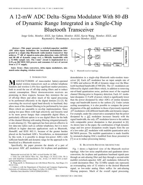
IEEE JOURNAL OF SOLID-STATE CIRCUITS, VOL. 37, NO. 3, MARCH 2002 271<br />
A <strong>12</strong>-<strong>mW</strong> <strong>ADC</strong> Delta–Sigma Modulator With <strong>80</strong> <strong>dB</strong><br />
<strong>of</strong> Dynamic Range Integrated in a Single-Chip<br />
Bluetooth Transceiver<br />
Jorge Grilo, Member, IEEE, Ian Galton, Member, IEEE, Kevin Wang, Member, IEEE, and<br />
Raymond G. Montemayor, Associate Member, IEEE<br />
Abstract—This paper presents a switched-capacitor multibit<br />
<strong>ADC</strong> <strong>delta</strong>–<strong>sigma</strong> <strong>modulator</strong> for baseband demodulation integrated<br />
in a single-chip Bluetooth radio-modem transceiver that<br />
achieves 77 <strong>dB</strong> <strong>of</strong> signal-to-noise-plus-distortion ratio (SINAD)<br />
and <strong>80</strong> <strong>dB</strong> <strong>of</strong> <strong>dynamic</strong> <strong>range</strong> over a 500-kHz bandwidth <strong>with</strong><br />
a 32-MHz sample rate. The 1-mm 2 circuit is implemented in a<br />
0.35- m BiCMOS SOI process and consumes 4.4 mA <strong>of</strong> current<br />
from a 2.7-V supply.<br />
Index Terms—Data converters, <strong>delta</strong>–<strong>sigma</strong> <strong>modulator</strong>s, mismatch<br />
noise shaping, wireless receiver.<br />
Fig. 1.<br />
Bluetooth receiver topology.<br />
I. INTRODUCTION<br />
MANUFACTURERS <strong>of</strong> mass-market battery-operated<br />
digital wireless transceivers such as cellular telephone<br />
handsets and wireless LANs face significant market pressures,<br />
both to avoid the use <strong>of</strong> <strong>of</strong>f-chip analog filters and to reduce<br />
current consumption. Direct downconversion receivers are<br />
promising in these respects, because they minimize the use<br />
<strong>of</strong> <strong>of</strong>f-chip filters and allow much <strong>of</strong> the signal processing<br />
to be performed efficiently in the digital domain [1]–[3]. By<br />
converting the received signal band directly to baseband, they<br />
allow most <strong>of</strong> the channel filtering to be performed by low-pass<br />
filters which are amenable to on-chip implementation. Since<br />
analog low-pass filters <strong>with</strong> high selectivity and linearity tend<br />
to be more power hungry than comparable digital filters, a<br />
particularly efficient option is to use digital filters for the bulk<br />
<strong>of</strong> the channel filtering <strong>with</strong> analog filtering relegated primarily<br />
to anti-aliasing [1]. This approach has been proven effective in<br />
low data-rate radios such as cellular telephones, but it is more<br />
difficult in higher data-rate applications such as Bluetooth,<br />
HomeRF, and IEEE <strong>80</strong>2.11, because <strong>of</strong> the greater burden<br />
placed on the baseband <strong>ADC</strong>s. Nevertheless, as demonstrated<br />
by this work, it is possible to design low-power <strong>ADC</strong>s <strong>with</strong><br />
sufficient bandwidth and <strong>dynamic</strong> <strong>range</strong> for the approach to be<br />
beneficial in a Bluetooth receiver.<br />
Specifically, the paper presents the details <strong>of</strong> a pair <strong>of</strong><br />
low-power <strong>ADC</strong> <strong>modulator</strong>s for in-phase and quadrature<br />
Manuscript received July 26, 2001; revised October 10, 2001.<br />
J. Grilo was <strong>with</strong> Silicon Wave Inc., San Diego, CA 92<strong>12</strong>2 USA. He is<br />
now <strong>with</strong> SolarFlare Communications, Inc., Irvine, CA 92618 USA (e-mail:<br />
jgrilo@solarflare.com).<br />
K. Wang and R. G. Montemayor are <strong>with</strong> Silicon Wave Inc., San Diego, CA<br />
92<strong>12</strong>2 USA.<br />
I. Galton is <strong>with</strong> the Department <strong>of</strong> Electrical and Computer Engineering,<br />
University <strong>of</strong> California at San Diego, La Jolla, CA 92093 USA.<br />
Publisher Item Identifier S 0018-9200(02)016<strong>80</strong>-3.<br />
demodulation in a single-chip Bluetooth radio-modem transceiver<br />
[4]. Each <strong>modulator</strong> has an input sample rate <strong>of</strong><br />
32 MHz and achieves <strong>80</strong> <strong>dB</strong> <strong>of</strong> <strong>dynamic</strong> <strong>range</strong> over the Bluetooth<br />
baseband bandwidth <strong>of</strong> 500 kHz. The <strong>modulator</strong>s are<br />
followed by digital comb filters which, in addition to removing<br />
out-<strong>of</strong>-band quantization noise, perform most <strong>of</strong> the required<br />
channel filtering prior to frequency detection. Each <strong>modulator</strong><br />
dissipates 11.9 <strong>mW</strong> <strong>of</strong> power, which is significantly lower<br />
than the power dissipated by other <strong>ADC</strong>s <strong>of</strong> similar <strong>dynamic</strong><br />
<strong>range</strong> and bandwidth known to the authors [5]. Under certain<br />
scaling assumptions, it is also possible to compare the power<br />
dissipation <strong>of</strong> the <strong>modulator</strong> to those <strong>of</strong> previously reported<br />
<strong>modulator</strong>s <strong>with</strong> different bandwidths and <strong>dynamic</strong> <strong>range</strong>s.<br />
For example, under the conservative assumption that the power<br />
dissipated by a <strong>modulator</strong> increases linearly <strong>with</strong> the<br />
signal bandwidth, the only <strong>modulator</strong> known to the authors<br />
<strong>with</strong> comparable power dissipation is that presented in [6].<br />
As shown later in the paper, the combination <strong>of</strong> high <strong>dynamic</strong><br />
<strong>range</strong> and low power dissipation results largely from the use<br />
<strong>of</strong> a low-order <strong>modulator</strong> <strong>with</strong> multibit quantization and a<br />
BiCMOS process. The multibit quantization is made feasible<br />
by mismatch-shaping DACs modified from those presented in<br />
[7] so as to reduce processing latency.<br />
II. BLUETOOTH RECEIVER ARCHITECTURE<br />
Fig. 1 shows a high-level view <strong>of</strong> the Bluetooth receiver<br />
topology. After low noise amplification and quadrature downconversion,<br />
the in-phase and quadrature baseband signals pass<br />
through an anti-aliasing filter and then through a second-order<br />
multibit switched-capacitor <strong>ADC</strong> <strong>modulator</strong>, followed by<br />
a comb decimation filter. The 32-MHz sample rate represents<br />
an oversampling ratio <strong>of</strong> 32 relative to the desired Bluetooth<br />
signal, so low-order analog filters suffice for anti-aliasing<br />
filtering purposes. Much <strong>of</strong> the overall signal processing,<br />
0018–9200/02$17.00 © 2002 IEEE
272 IEEE JOURNAL OF SOLID-STATE CIRCUITS, VOL. 37, NO. 3, MARCH 2002<br />
Fig. 2.<br />
Simplified block diagram <strong>of</strong> the 16 <strong>modulator</strong>.<br />
including channel filtering, frequency demodulation, and clock<br />
and data recovery, is performed in the digital domain.<br />
III. DELTA–SIGMA MODULATOR TOPOLOGY<br />
A. Comparison <strong>of</strong> Different Architecture Candidates<br />
Fig. 2 shows the simplified block diagram <strong>of</strong> the<br />
<strong>modulator</strong>. It is a second-order structure <strong>with</strong> two delaying<br />
discrete-time integrators and a 17-level quantizer surrounded<br />
by two feedback loops [8]. With ideal components and a sample<br />
rate <strong>of</strong> 32 MHz, it has a <strong>dynamic</strong> <strong>range</strong> <strong>of</strong> 87 <strong>dB</strong> over the<br />
0–500-kHz frequency band.<br />
The use <strong>of</strong> a low-order <strong>modulator</strong> <strong>with</strong> multibit quantization<br />
made possible the low current consumption and high<br />
<strong>dynamic</strong> <strong>range</strong> achieved by the circuit. Although a higher order<br />
single-loop architecture <strong>with</strong> one-bit quantization or a MASH<br />
architecture could have been used instead, as outlined in this<br />
section, such solutions would have resulted in higher current<br />
consumption.<br />
To maintain stability <strong>with</strong> one-bit quantization, the pole and<br />
zero placement in single-loop high-order <strong>modulator</strong>s is<br />
highly constrained. This generally results in less aggressive<br />
quantization noise shaping, thereby necessitating higher order<br />
loops, and a lower input no-overload <strong>range</strong> than is possible<br />
<strong>with</strong> multibit quantization. For instance, to achieve the necessary<br />
in-band <strong>dynamic</strong> <strong>range</strong> for the given frequency plan<br />
and application described in this paper, a sixth-order<br />
<strong>modulator</strong>, typically requiring six opamps, would have been<br />
necessary [9]. The lower input no-overload <strong>range</strong> generally<br />
necessitates larger input sampling capacitors to achieve a given<br />
signal-to-thermal-noise ratio, and this gives rise to opamp<br />
designs <strong>with</strong> greater current consumption.<br />
MASH structures became popular for high-<strong>dynamic</strong> <strong>range</strong><br />
applications because they facilitate higher order loops that<br />
do not suffer from stability problems. However, they rely on<br />
good matching between analog and digital transfer functions;<br />
in the presence <strong>of</strong> mismatches, quantization noise from the<br />
front-end stages appears at the output. Moreover, these structures<br />
are characterized by an inherent loss in <strong>dynamic</strong> <strong>range</strong> due<br />
to internal signal scaling. These two factors impose constraints<br />
on the minimum size that can be used for capacitors, and hence<br />
on the minimum current consumption that can be achieved. A<br />
popular structure consists <strong>of</strong> a second-order single-loop <strong>modulator</strong><br />
followed by a first-order <strong>modulator</strong>. Although practical,<br />
the structure requires three opamps, and the last stage opamp<br />
sums three input signals, thereby increasing its capacitive load,<br />
and hence its current consumption.<br />
In contrast, the multibit second-order architecture used in the<br />
circuit presented here requires only two opamps. Furthermore,<br />
its no-overload <strong>range</strong> is nearly equal to its reference voltage,<br />
which allows for smaller input sampling capacitors compared<br />
to the other architectures, and hence opamps <strong>with</strong> lower current<br />
consumption. As described in the next section, the architecture<br />
does require a significant amount <strong>of</strong> digital logic to implement<br />
the mismatch-shaping DACs, but the current consumed by this<br />
logic is small compared to the current consumed by the rest <strong>of</strong><br />
the circuit. This trend is further supported by migration to small<br />
feature processes.<br />
IV. CIRCUIT DESIGN<br />
A. Switched-Capacitor Top-Level Design<br />
Fig. 3 shows the simplified circuit schematic <strong>of</strong> the <strong>modulator</strong>.<br />
To accommodate a low power supply voltage <strong>with</strong> good<br />
sampling switch performance, the input common-mode voltage<br />
<strong>of</strong> the operational amplifiers was set at 1 V. This low value<br />
permitted the use <strong>of</strong> small, single n-channel devices for accurate<br />
definition <strong>of</strong> the sampling time.<br />
The design uses a negative reference voltage, that is,<br />
, where the common-mode voltage<br />
V and<br />
V. This allows the use <strong>of</strong> small sampling<br />
switches and results in low reference noise power (11 V ).<br />
The reference voltage is derived from a resistive division <strong>of</strong> a<br />
bandgap voltage reference circuit. Since the reference value is<br />
small, the noise due to the resistors is low. To reduce the effect<br />
<strong>of</strong> signal-dependent charge injection onto the reference and<br />
charge injection due to component mismatches, a cross-sampling<br />
scheme was used. Moreover, delayed clock phases were<br />
used where appropriate.<br />
The scaling coefficients were chosen in order to meet<br />
three main objectives. The first objective was to confine the<br />
internal signals to the high-gain, most linear region <strong>of</strong> the<br />
amplifiers. The second objective was to comply <strong>with</strong> the input<br />
common-mode requirements <strong>of</strong> the comparators in the internal<br />
flash <strong>ADC</strong>. These, too, imposed restrictions on the maximum<br />
signal swing allowed at the output <strong>of</strong> the second integrator. The<br />
third objective was to provide optimum, equal loading conditions<br />
for the first opamp in both clock phases in conjunction<br />
<strong>with</strong> a suitable choice <strong>of</strong> the input capacitor size. A factor that<br />
determined the final value <strong>of</strong> the input capacitor was<br />
noise power, in particular the partition <strong>of</strong> noise contribution<br />
<strong>with</strong>in the <strong>ADC</strong> toward the total noise power budget. The total<br />
integrated noise (0–500 kHz) arising from the switches<br />
on-resistance is 45 V , resulting in about 3-<strong>dB</strong> degradation<br />
<strong>of</strong> the noise floor when added to the quantization noise.<br />
The output <strong>of</strong> the second integrator is sampled and quantized<br />
into a 17-level representation. The quantizer produces a 16-bit<br />
thermometer code output, which is supplied to the feedback mismatch<br />
noise shaper digital encoder for further processing, and<br />
then to the feedback DACs. A binary encoder also converts the<br />
thermometer code to a more convenient 5-bit digital representation.<br />
The output <strong>of</strong> this binary encoder constitutes the “output”<br />
<strong>of</strong> the <strong>modulator</strong>, and is fed to a decimation filter for removal<br />
<strong>of</strong> out-<strong>of</strong>-band noise, and then to a GFSK de<strong>modulator</strong>.
GRILO et al.: A <strong>12</strong>-<strong>mW</strong> <strong>ADC</strong> DELTA–SIGMA MODULATOR 273<br />
Fig. 3.<br />
Simplified circuit diagram <strong>of</strong> the 16 <strong>modulator</strong>.<br />
Fig. 4.<br />
Simplified opamp schematic.<br />
Four identical DACs were used in the feedback path, each<br />
<strong>with</strong> 16 unit capacitors, <strong>with</strong> a total capacitance equal to the<br />
value <strong>of</strong> input capacitor (0.5 pF). The use <strong>of</strong> two DACs to<br />
implement the feedback path effectively realizes a coefficient<br />
<strong>of</strong> two, necessary for loop stability and for the noise shaping<br />
function. Although the inner loop feedback DAC total capacitance<br />
could be made smaller, its value was also constrained<br />
by the equal loading requirement for the first opamp. The total<br />
capacitance in the inner DAC and the second-stage scaling<br />
coefficients determine the load <strong>of</strong> the first opamp during the<br />
sampling phase.<br />
B. Operational Amplifier<br />
Fig. 4 shows the circuit diagram <strong>of</strong> the operational amplifier.<br />
To take advantage <strong>of</strong> the availability <strong>of</strong> bipolar devices, a<br />
two-stage Miller-compensated configuration was chosen.<br />
Using bipolar devices in the second stage results in ease <strong>of</strong><br />
phase compensation at very modest current levels. (In an<br />
all-CMOS design, the second stage is typically notorious for<br />
consuming excessive current to achieve suitable phase margin.)<br />
A two-stage opamp is also more amenable for low-voltage<br />
design [10].<br />
Conforming to a low value <strong>of</strong> the input common-mode<br />
voltage, the input stage <strong>of</strong> the amplifiers employed p-channel<br />
devices, <strong>with</strong> the added benefit <strong>of</strong> lower noise. However,<br />
the latter aspect <strong>of</strong> the design did not receive much importance,<br />
as GFSK demodulation de-emphasizes low frequency noise.<br />
Moreover, the hopping frequency in Bluetooth is 1.6 kHz, and<br />
hence no significant energy exists below that frequency. (This<br />
applies for DH1 packets. For DH5 packets, the hopping frequency<br />
can be as low as 533 Hz; however, DH5 packets imply<br />
large signals, and sensitivity is not an issue.) The simulated<br />
integrated opamp noise in the band (1–500 kHz) was 20 V ,<br />
making it the main noise contributor (60%).<br />
The opamp was designed to have a dc gain <strong>of</strong> <strong>80</strong> <strong>dB</strong>, a<br />
unity-gain frequency <strong>of</strong> 350 MHz, and a phase margin <strong>of</strong><br />
<strong>80</strong> , in both clock phases. The amplifier uses a conventional<br />
switched-capacitor network to set the output common-mode<br />
voltage at 1.35 V.<br />
C. Comparator Used in the Flash <strong>ADC</strong><br />
Fig. 5 shows the circuit diagram <strong>of</strong> the comparators used in<br />
the internal flash <strong>ADC</strong>. The use <strong>of</strong> bipolar devices at the input<br />
stage resulted in a design <strong>with</strong> low input-referred <strong>of</strong>fset, at low<br />
current levels. This is attributable to the inherently low <strong>of</strong>fset <strong>of</strong><br />
the bipolar devices, and to their large transconductance, relative<br />
to that <strong>of</strong> the p-channel load devices. The estimated standard<br />
deviation <strong>of</strong> the input-referred <strong>of</strong>fset is 4 mV.<br />
The comparator structure employs resetting to reduce hysteresis.<br />
In particular, during phase the outputs are shorted<br />
to ground, and hence it is necessary for proper operation <strong>of</strong> the<br />
<strong>modulator</strong> to hold the outputs for a full clock cycle. For that<br />
purpose, the topology requires static latches at the output. Such<br />
latches, however, were not used at this point for reasons that will<br />
be addressed later in the paper.
274 IEEE JOURNAL OF SOLID-STATE CIRCUITS, VOL. 37, NO. 3, MARCH 2002<br />
Fig. 5.<br />
Comparator used in the internal flash <strong>ADC</strong>.<br />
Fig. 6.<br />
Generalized block diagram <strong>of</strong> a 17-level DAC.<br />
(a)<br />
D. The Feedback Path<br />
Fig. 6 shows a simplified block diagram <strong>of</strong> a generalized<br />
17-level digital-to-analog converter. It consists <strong>of</strong> a digital encoder<br />
followed by a bank <strong>of</strong> 16 one-bit DACs whose analog outputs<br />
are summed to generate the overall output, . The input<br />
sequence, , is restricted to the set { 8, 7, 8, 8}. During<br />
each sample interval the digital encoder sets 8 <strong>of</strong> its<br />
output bits high and 8 <strong>of</strong> its output bits low. Each one-bit<br />
DAC generates an analog output given by if its input<br />
bit is high, and if its input bit is low, where and<br />
are the high and low one-bit DAC errors, respectively. The<br />
DAC errors are assumed to result primarily from static component<br />
mismatches. Thus, if there were no mismatches, the output<br />
<strong>of</strong> the DAC would be . As shown in [11], in this case the<br />
overall DAC output has the form<br />
where is a constant gain, is a constant <strong>of</strong>fset, and is<br />
DAC noise that depends upon the input sequence and the one-bit<br />
DAC errors in general. The purpose <strong>of</strong> the digital encoder is to<br />
cause to be white or spectrally shaped as required by<br />
the application. For the present application, the digital encoder<br />
is designed to suppress the power <strong>of</strong> the DAC noise in the frequency<br />
band below 500 kHz, so it is referred to as a mismatch<br />
noise shaping digital encoder.<br />
The mismatch noise shaping digital encoder consists <strong>of</strong> digital<br />
logic blocks, called switching blocks, organized in a tree<br />
structure as shown in Fig. 7(a) [11]. Each switching block partitions<br />
its input sequence into two output sequences according to<br />
a prescribed algorithm. Fig. 7(b) shows the details <strong>of</strong> the<br />
switching block. It contains a swapper cell that permutes the<br />
input bits according to the value <strong>of</strong> the th bit in the sequence<br />
. This sequence is a function <strong>of</strong> the input signal through<br />
(b)<br />
Fig. 7. (a) Mismatch noise shaping digital encoder. (b) Implementation details<br />
<strong>of</strong> the S switching block.<br />
a parity detector, and some additional processing. As shown in<br />
[7] and [11], this configuration results in a distortion component<br />
given by<br />
where<br />
constant<br />
if<br />
if<br />
otherwise.<br />
and<br />
Therefore, the DAC noise inherits the properties <strong>of</strong> the<br />
switching sequences, . It can be shown that the circuit<br />
consisting <strong>of</strong> two flip-flops shown in Fig. 7(b) generates a
GRILO et al.: A <strong>12</strong>-<strong>mW</strong> <strong>ADC</strong> DELTA–SIGMA MODULATOR 275<br />
Fig. 8.<br />
Connection <strong>of</strong> the swapper cells and parity detection.<br />
Fig. 10.<br />
Timing diagram.<br />
Fig. 9.<br />
The shift <strong>of</strong> the latching function <strong>with</strong> the purpose <strong>of</strong> reducing latency.<br />
sequence whose integral is bounded, which is a sufficient<br />
condition for the power spectral density to be zero at dc, which<br />
for this case implies first-order high-pass spectral shaping.<br />
Hence, the DAC noise is also first-order noise shaped. (Analogously,<br />
th-order noise shaping can be achieved by generating<br />
sequences whose th integral is bounded.)<br />
All mismatch noise shaping digital encoders suffer from the<br />
inherent shortcoming that they introduce additional delay to the<br />
overall DAC. The delay increases linearly <strong>with</strong> the number <strong>of</strong><br />
bits, which can be particularly problematic in high data rate systems.<br />
For proper operation, the signal must propagate around the<br />
feedback loop in a period <strong>of</strong> time much shorter than half a clock<br />
cycle or it will generate glitches that disturb the settling <strong>of</strong> the<br />
amplifiers. In contrast, the parity detection mechanism does not<br />
have to be fast, as the information generated in one clock cycle<br />
is used only during the next one.<br />
To reduce the latency through the mismatch noise shaping<br />
digital encoder, the swapper cells were implemented <strong>with</strong> minimum-size<br />
CMOS transmission gates. Although the resulting<br />
switching blocks perform the same mathematical operations as<br />
those presented in [7], the use <strong>of</strong> transmission gates instead <strong>of</strong><br />
conventional digital logic allowed a significant reduction in the<br />
propagation delay. The parity detection was done a posteriori,<br />
in the following clock cycle, utilizing an inverted tree <strong>of</strong> XOR<br />
gates whose outputs contain the parity information to be used<br />
in their respective layers (Fig. 8). To further reduce the latency<br />
through the feedback loop, the latching function required to<br />
hold the output <strong>of</strong> the flash <strong>ADC</strong> comparators for a full clock<br />
cycle was moved to the outputs <strong>of</strong> the mismatch noise shaping<br />
digital encoder and binary encoder (Fig. 9). These measures<br />
facilitated a reduction <strong>of</strong> the propagation delay between the<br />
clock edge that commands the update <strong>of</strong> each comparator output<br />
in the <strong>ADC</strong> and the corresponding edge at the output <strong>of</strong> the<br />
feedback DACs to 1 ns. Fig. 10 shows the timing diagram<br />
<strong>of</strong> critical events.
276 IEEE JOURNAL OF SOLID-STATE CIRCUITS, VOL. 37, NO. 3, MARCH 2002<br />
Fig. 11. Simulated output spectrum when the mismatch noise shaper is<br />
enabled and disabled.<br />
Fig. 13. Measured signal-to-noise-plus-distortion ratio for a 31.25-kHz<br />
sinusoidal input signal.<br />
Fig. 14.<br />
Chip photograph.<br />
Fig. <strong>12</strong>.<br />
Measured output spectrum.<br />
E. Simulated Results<br />
Fig. 11 shows the simulated output spectrum <strong>of</strong> the <strong>modulator</strong><br />
for a 1.31 V , 31.25-kHz sinusoidal input signal, using an<br />
estimated 0.3% matching among the feedback DAC elements.<br />
Also shown is the result <strong>of</strong> disabling the mismatch noise shaper<br />
digital encoder, <strong>with</strong> the same simulation parameters. While<br />
the former achieves a peak signal-to-noise-plus-distortion ratio<br />
(SINAD) <strong>of</strong> 81 <strong>dB</strong>, the latter is limited to about 64 <strong>dB</strong> due to<br />
harmonic distortion. This figure clearly demonstrates the effectiveness<br />
<strong>of</strong> the technique. The simulation included the equivalent<br />
input-referred noise due to the opamp, , and reference<br />
noise.<br />
V. EXPERIMENTAL RESULTS<br />
Fig. <strong>12</strong> shows the measured output spectrum, which can be<br />
compared <strong>with</strong> the simulated results in Fig. 11. The signal applied<br />
possessed the same amplitude and frequency as the one<br />
used in simulations. The peak SINAD is only 77 <strong>dB</strong>, rather than<br />
81 <strong>dB</strong>, which is attributable mostly to a certain degree <strong>of</strong> current<br />
starvation in the opamps and <strong>of</strong>fsets in the flash <strong>ADC</strong>. The<br />
noise floor is in agreement <strong>with</strong> the simulated result. Although<br />
not shown, disabling the mismatch noise shaper digital encoder<br />
produced results <strong>with</strong>in 2 <strong>dB</strong> <strong>of</strong> the simulation, supporting the<br />
earlier estimation <strong>of</strong> capacitor mismatches.<br />
Fig. 13 shows the measured SINAD again for a 31.25-kHz<br />
input signal frequency. This curve shows a <strong>dynamic</strong> <strong>range</strong> <strong>of</strong><br />
<strong>80</strong> <strong>dB</strong> and a peak SINAD <strong>of</strong> about 77 <strong>dB</strong>. Note that the SINAD<br />
stops increasing linearly <strong>with</strong> the input signal power at about 6<br />
<strong>dB</strong>V, due to the distortion mechanisms mentioned above, not<br />
due to quantization noise. Although the measurements shown<br />
here were done <strong>with</strong> a relatively low frequency input signal, no<br />
observable differences were noted for higher frequencies, both<br />
in our measurements and in system-level measurements. These<br />
measurements were done <strong>with</strong> a 2.7-V power supply, and the<br />
measured current was 4.4 mA.<br />
Fig. 14 shows the die photograph <strong>of</strong> one channel, <strong>with</strong> indication<br />
<strong>of</strong> the location <strong>of</strong> each main block. (The second channel<br />
is a mirrored version around the bottom horizontal axis.) The<br />
total area shown is about 1 mm .<br />
Table I summarizes the performance <strong>of</strong> the <strong>modulator</strong>, and<br />
Table II its current consumption breakdown. Most <strong>of</strong> the current<br />
was consumed in the analog circuitry.
GRILO et al.: A <strong>12</strong>-<strong>mW</strong> <strong>ADC</strong> DELTA–SIGMA MODULATOR 277<br />
TABLE I<br />
SUMMARY OF THE PERFORMANCE OF THE MODULATOR<br />
[8] G. Lainey, R. Saintlaurens, and P. Senn, “Switched-capacitor secondorder<br />
noise-shaping coder,” Electron. Lett., vol. 19, pp. 149–150, Feb.<br />
1983.<br />
[9] R. Schreier, “An empirical study <strong>of</strong> high-order, single-bit <strong>delta</strong>–<strong>sigma</strong><br />
<strong>modulator</strong>s,” IEEE Trans. Circuits Syst. II, vol. 40, pp. 461–466, Aug.<br />
1993.<br />
[10] J. Grilo, E. MacRobbie, R. Halim, and G. C. Temes, “A 1.8 V 94 <strong>dB</strong><br />
<strong>dynamic</strong> <strong>range</strong> 16 <strong>modulator</strong> for voice applications,” in Proc. IEEE<br />
Int. Solid-State Circuits Conf., vol. 39, 1996, pp. 230–231.<br />
[11] I. Galton, “Spectral shaping <strong>of</strong> circuit errors in digital-to-analog converters,”<br />
IEEE Trans. Circuits Syst. II, vol. 44, pp. <strong>80</strong>8–817, Nov. 1997.<br />
TABLE II<br />
CURRENT CONSUMPTION STRUCTURE<br />
VI. CONCLUSIONS<br />
The implementation details <strong>of</strong> a <strong>delta</strong>–<strong>sigma</strong> <strong>modulator</strong> <strong>ADC</strong><br />
for quadrature baseband demodulation integrated in a commercial<br />
direct-conversion Bluetooth radio-modem transceiver have<br />
been presented. The design achieves <strong>80</strong> <strong>dB</strong> <strong>of</strong> <strong>dynamic</strong> <strong>range</strong><br />
and 77 <strong>dB</strong> <strong>of</strong> peak SINAD over the 0–500 kHz Bluetooth signal<br />
bandwidth, <strong>with</strong> a current consumption <strong>of</strong> 4.4 mA. The low current<br />
consumption was made possible through the use <strong>of</strong> multibit<br />
quantization, which permitted the use <strong>of</strong> a low-order singlestage<br />
<strong>delta</strong>–<strong>sigma</strong> <strong>modulator</strong> <strong>with</strong> relaxed opamp requirements,<br />
and innovations in the design <strong>of</strong> the feedback path components,<br />
including the mismatch-shaping DAC logic so as to minimize<br />
latency. Judicious use <strong>of</strong> n-p-n bipolar transistors in the opamps<br />
and comparators also resulted in current savings relative to that<br />
which would likely be achieved in a comparable fully CMOS<br />
design.<br />
ACKNOWLEDGMENT<br />
The authors would like to thank E. Yang for technical support<br />
during measurements.<br />
REFERENCES<br />
[1] J. St<strong>range</strong> and S. Atkinson, “A direct conversion transceiver for multiband<br />
GSM application,” in IEEE RFIC Symp. Dig. Papers, June 2000,<br />
pp. 25–28.<br />
[2] C. D. Hull, J. L. Tham, and R. R. Chu, “A direct-conversion receiver<br />
for 900 MHz (ISM band) spread-spectrum digital cordless telephone,”<br />
IEEE J. Solid-State Circuits, vol. 31, pp. 1955–1963, Dec. 1996.<br />
[3] A. Abidi, “Direct conversion radio transceivers for digital communication,”<br />
IEEE J. Solid-State Circuits, vol. 30, pp. 1399–1410, Dec. 1995.<br />
[4] “SiW1502 Bluetooth radio modem IC data sheet,” Silicon Wave, Nov.<br />
3, 2000.<br />
[5] R. H. Walden, “Analog-to-digital converter survey and analysis,” IEEE<br />
J. Select. Areas Commun., vol. 17, pp. 539–550, Apr. 1999.<br />
[6] O. Oliaei, P. Clement, and P. Gorisse, “A 5 <strong>mW</strong> 61 <strong>modulator</strong> <strong>with</strong><br />
84<strong>dB</strong> <strong>dynamic</strong> <strong>range</strong> for GSM/EDGE,” in Proc. ISSCC, 2001, pp.<br />
46–47, 428.<br />
[7] E. Fogleman, I. Galton, W. Huff, and H. T. Jensen, “A 3.3V single-poly<br />
CMOS audio <strong>ADC</strong> <strong>delta</strong>–<strong>sigma</strong> <strong>modulator</strong> <strong>with</strong> 98-<strong>dB</strong> peak SINAD and<br />
105<strong>dB</strong> peak SFDR,” IEEE J. Solid-State Circuits, vol. 35, pp. 297–307,<br />
Mar. 2000.<br />
Jorge Grilo (S’93–M’97) received the Diploma from<br />
the Instituto Superior Técnico, Lisbon, Portugal, in<br />
1991, and the M.S. and Ph.D. degrees from Oregon<br />
State University, Corvallis, in 1994 and 1997, respectively,<br />
all in electrical engineering.<br />
From 1994 through 1998, he was <strong>with</strong> Rockwell<br />
Semiconductor Systems, Newport Beach, CA,<br />
where he designed mixed-signal integrated circuits<br />
for communications. From 1998 through 2001, he<br />
was <strong>with</strong> Silicon Wave, San Diego, CA, where he<br />
designed mixed-signal and RF integrated circuits for<br />
wireless communications. Since 2001, he has been a Member <strong>of</strong> the Technical<br />
Staff <strong>with</strong> Solarflare Communications, Irvine, CA, where he designs integrated<br />
circuits for high-speed wireline communications. His interests include signal<br />
processing techniques, semiconductor devices, high-speed data converters, and<br />
RF circuits for communications.<br />
Dr. Grilo is an Associate Editor <strong>of</strong> the IEEE TRANSACTIONS ON CIRCUITS<br />
AND SYSTEMS II.<br />
Ian Galton (M’92) received the Sc.B. degree from<br />
Brown University, Providence, RI, in 1984, and the<br />
M.S. and Ph.D. degrees from the California Institute<br />
<strong>of</strong> Technology, Pasadena, in 1989 and 1992, respectively,<br />
all in electrical engineering.<br />
Since 1996, he has been an Associate Pr<strong>of</strong>essor <strong>of</strong><br />
electrical engineering at the University <strong>of</strong> California,<br />
San Diego, where he teaches and conducts research<br />
in the field <strong>of</strong> mixed-signal integrated circuits and<br />
systems for communications. Prior to 1996, he was<br />
<strong>with</strong> the University <strong>of</strong> California, Irvine, the NASA<br />
Jet Propulsion Laboratory, Acuson, and Mead Data Central. Pr<strong>of</strong>essor Galton’s<br />
research involves the invention, analysis, and integrated circuit implementation<br />
<strong>of</strong> key communication system blocks such as data converters, frequency synthesizers,<br />
and clock recovery systems. The emphasis <strong>of</strong> the research is on the<br />
development <strong>of</strong> digital signal processing techniques to mitigate the effects <strong>of</strong><br />
nonideal analog circuit behavior <strong>with</strong> the objective <strong>of</strong> generating enabling technology<br />
for highly integrated low-cost communication systems. In addition to his<br />
academic research, he regularly consults at several communications and semiconductor<br />
companies and teaches portions <strong>of</strong> various industry-oriented short<br />
courses on the design <strong>of</strong> data converters, PLLs, and wireless transceivers. He<br />
has served on a corporate Board <strong>of</strong> Directors and several Technical Advisory<br />
Boards.<br />
Dr. Galton is a member <strong>of</strong> the IEEE Circuits and Systems Society Board <strong>of</strong><br />
Governors, and is the Editor-in-Chief <strong>of</strong> the IEEE TRANSACTIONS ON CIRCUITS<br />
AND SYSTEMS II.<br />
Kevin Wang (M’98) received the B.S. degree from<br />
Cornell University, Ithaca, NY, in 1995, and the M.S.<br />
degree from the University <strong>of</strong> California, Berkeley, in<br />
1998, all in electrical engineering.<br />
Since 1998, he has been a Member <strong>of</strong> the Technical<br />
Staff at Silicon Wave, San Diego, CA, where he<br />
designs mixed-signal circuits. His interests include<br />
analog and digital circuit design as well as CAD development.
278 IEEE JOURNAL OF SOLID-STATE CIRCUITS, VOL. 37, NO. 3, MARCH 2002<br />
Raymond G. Montemayor (S’94–A’96) was born in<br />
Los Angeles, CA, in 1974. He received the B.S. degree<br />
in engineering in 1996 from Harvey Mudd College,<br />
Claremont, CA. He is currently working toward<br />
the M.S. degree in electrical engineering at the University<br />
<strong>of</strong> California, Los Angeles. His research work<br />
is on a self-calibrating image-reject receiver implemented<br />
in CMOS.<br />
Since 1998, he has been <strong>with</strong> Silicon Wave, Inc.,<br />
San Diego, CA, where he designs analog and RF integrated<br />
circuits for wireless and wireline communication<br />
systems-on-chip.