Techniques for in-band phase noise suppression in re-circulating ...
Techniques for in-band phase noise suppression in re-circulating ...
Techniques for in-band phase noise suppression in re-circulating ...

You also want an ePaper? Increase the reach of your titles
YUMPU automatically turns print PDFs into web optimized ePapers that Google loves.
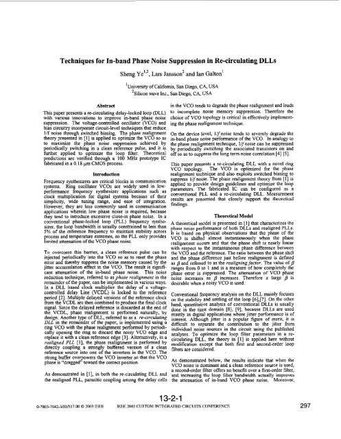
<strong>Techniques</strong> <strong>for</strong> In-<strong>band</strong> Phase Noise Supp<strong>re</strong>ssion <strong>in</strong> Re-circulat<strong>in</strong>g DLLsAbstractThis paper p<strong>re</strong>sents a <strong>re</strong>-circulat<strong>in</strong>g delay-locked loop @LL)with various <strong>in</strong>novations to improve <strong>in</strong>-<strong>band</strong> <strong>phase</strong> <strong>noise</strong><strong>supp<strong>re</strong>ssion</strong>. The voltage-controlled oscillator @’CO) andbias circuitry <strong>in</strong>corporate circuit-level techniques that <strong>re</strong>ducel/f <strong>noise</strong> through switched bias<strong>in</strong>g. The <strong>phase</strong> <strong>re</strong>alignmenttheory p<strong>re</strong>sented <strong>in</strong> [I] is applied to optimize the VCO so asto maximize the <strong>phase</strong> <strong>noise</strong> <strong>supp<strong>re</strong>ssion</strong> achieved byperiodically switch<strong>in</strong>g <strong>in</strong> a clean <strong>re</strong>fe<strong>re</strong>nce pulse, and it isfurther applied to optimize the loop filter. Theo<strong>re</strong>ticalp<strong>re</strong>dictions a<strong>re</strong> verified through a 100 MHz prototype ICfabricated <strong>in</strong> a 0.18 p~ CMOS process.IntroductionF<strong>re</strong>quency synthesizers a<strong>re</strong> critical blocks <strong>in</strong> communicationsystems. R<strong>in</strong>g oscillator VCOs a<strong>re</strong> widely used <strong>in</strong> lowper<strong>for</strong>mancef<strong>re</strong>quency synthesizer applications such asclock multiplication <strong>for</strong> digital systems because of theirsimplicity, wide tun<strong>in</strong>g range, and ease of <strong>in</strong>tegration.However, they a<strong>re</strong> less commonly used <strong>in</strong> communicationapplications whe<strong>re</strong><strong>in</strong> low <strong>phase</strong> <strong>noise</strong> is <strong>re</strong>qui<strong>re</strong>d, becausethey tend to <strong>in</strong>troduce excessive close-<strong>in</strong> <strong>phase</strong> <strong>noise</strong>. In aconventional <strong>phase</strong>-locked loop (PLL) f<strong>re</strong>quency synthesizer,the loop <strong>band</strong>width is usually constra<strong>in</strong>ed to less than5% of the <strong>re</strong>fe<strong>re</strong>nce f<strong>re</strong>quency to ma<strong>in</strong>ta<strong>in</strong> stability acrossprocess and temperatu<strong>re</strong> ext<strong>re</strong>mes, so the PLL only provideslimited attenuation of the VCO <strong>phase</strong> <strong>noise</strong>.To overcome this barrier, a clean <strong>re</strong>fe<strong>re</strong>nce pulse can be<strong>in</strong>jected periodically <strong>in</strong>to the VCO so as to <strong>re</strong>set the <strong>phase</strong>error and the<strong>re</strong>by supp<strong>re</strong>ss the <strong>noise</strong> memoty caused by thejitter accumulation effect <strong>in</strong> the VCO. The <strong>re</strong>sult is signifi-cant attenuation of the <strong>in</strong>-<strong>band</strong> <strong>phase</strong> <strong>noise</strong>. This <strong>noise</strong><strong>re</strong>duction technique, <strong>re</strong>fer<strong>re</strong>d to as <strong>phase</strong> <strong>re</strong>alignment <strong>in</strong> the<strong>re</strong>ma<strong>in</strong>der of the paper, can be implemented <strong>in</strong> various ways.In a DLL based clock multiplier the delay of a voltagecontrolleddelay L<strong>in</strong>e (VCDL) is locked to the <strong>re</strong>fe<strong>re</strong>nceperiod [2]. Multiple delayed versions of the <strong>re</strong>fe<strong>re</strong>nce clockfrom the VCDL a<strong>re</strong> then comb<strong>in</strong>ed to produce the f<strong>in</strong>al clocksignal. S<strong>in</strong>ce the delayed <strong>re</strong>fe<strong>re</strong>nce is discarded at the end ofthe VCDL, <strong>phase</strong> <strong>re</strong>alignment is per<strong>for</strong>med naturally, bydesign. Another type of DLL, <strong>re</strong>fer<strong>re</strong>d to as a <strong>re</strong>-circulat<strong>in</strong>gDLL <strong>in</strong> the <strong>re</strong>ma<strong>in</strong>der of the paper, is implemented us<strong>in</strong>g ar<strong>in</strong>g VCO with the <strong>phase</strong> <strong>re</strong>alignment per<strong>for</strong>med by periodicallyopen<strong>in</strong>g the r<strong>in</strong>g to discard the noisy VCO edge and<strong>re</strong>place it with a clean <strong>re</strong>fe<strong>re</strong>nce edge [3]. Alternatively, <strong>in</strong> a<strong>re</strong>aligned PLL [I], the <strong>phase</strong> <strong>re</strong>alignment is per<strong>for</strong>med bydi<strong>re</strong>ctly coupl<strong>in</strong>g a strongly buffe<strong>re</strong>d version of a clean<strong>re</strong>fe<strong>re</strong>nce source <strong>in</strong>to one of the <strong>in</strong>verters <strong>in</strong> the VCO. Thestrong buffer overpowers the VCO <strong>in</strong>verter so that the VCO<strong>phase</strong> is “dragged” toward the cor<strong>re</strong>ct position.As demonstrated <strong>in</strong> [I], <strong>in</strong> both the <strong>re</strong>-circulat<strong>in</strong>g DLL andthe <strong>re</strong>aligned PLL, parasitic coupl<strong>in</strong>g among the delay cellsSheng Ye”*, Lars Jansson2 and Ian Galton’1University of Califomia, San Diego, CA, USA2Silicon wave Inc., San Diego, CA, USA<strong>in</strong> the VCO tends to degrade the <strong>phase</strong> <strong>re</strong>alignment and leadsto <strong>in</strong>complete <strong>noise</strong> memory <strong>supp<strong>re</strong>ssion</strong>. The<strong>re</strong><strong>for</strong>e thechoice of VCO topology is critical <strong>in</strong> effectively implement<strong>in</strong>gthe <strong>phase</strong> <strong>re</strong>alignment technique.On the device level, llf<strong>noise</strong> tends to seve<strong>re</strong>ly degrade the<strong>in</strong>-<strong>band</strong> <strong>phase</strong> <strong>noise</strong> per<strong>for</strong>mance of the VCO. In analogy tothe <strong>phase</strong> <strong>re</strong>alignment technique, llf<strong>noise</strong> can be supp<strong>re</strong>ssedby periodically switch<strong>in</strong>g the associated transistors on andoff so as to supp<strong>re</strong>ss the long term <strong>noise</strong> cor<strong>re</strong>lation [4] [5].This paper p<strong>re</strong>sents a <strong>re</strong>-circulat<strong>in</strong>g DLL with a novel r<strong>in</strong>gVCO topology. The VCO is optimized <strong>for</strong> the <strong>phase</strong><strong>re</strong>alignment technique and also exploits switched bias<strong>in</strong>g tosupp<strong>re</strong>ss llf<strong>noise</strong>. The <strong>phase</strong> <strong>re</strong>alignment theory from [I] isapplied to provide design guidel<strong>in</strong>es and optimize the loopparameters. The fabricated IC can be configu<strong>re</strong>d as aconventional PLL and a <strong>re</strong>-circulat<strong>in</strong>g DLL. Measu<strong>re</strong>ment<strong>re</strong>sults a<strong>re</strong> p<strong>re</strong>sented that closely support the theo<strong>re</strong>ticalf<strong>in</strong>d<strong>in</strong>gs.Theo<strong>re</strong>tical ModelA theo<strong>re</strong>tical model is p<strong>re</strong>sented <strong>in</strong> [I] that characterizes the<strong>phase</strong> <strong>noise</strong> per<strong>for</strong>mance of both DLLs and <strong>re</strong>aligned PLLs.It is based on physical observations that the <strong>phase</strong> of theVCO is shifted almost <strong>in</strong>stantaneously when the <strong>phase</strong><strong>re</strong>alignment occurs and that the <strong>phase</strong> shift is nearly l<strong>in</strong>earwith <strong>re</strong>spect to the <strong>in</strong>stantaneous <strong>phase</strong> diffe<strong>re</strong>nce betweenthe VCO and the <strong>re</strong>fe<strong>re</strong>nce. The ratio between the <strong>phase</strong> shiftand the <strong>phase</strong> diffe<strong>re</strong>nce just be<strong>for</strong>e <strong>re</strong>alignment is def<strong>in</strong>edas p and <strong>re</strong>fer<strong>re</strong>d to as the <strong>re</strong>align<strong>in</strong>g factor. The value of pranges from 0 to 1 and is a measu<strong>re</strong> of how completely the<strong>phase</strong> error is supp<strong>re</strong>ssed. The attenuation of VCO <strong>phase</strong><strong>noise</strong> <strong>in</strong>c<strong>re</strong>ases as p <strong>in</strong>c<strong>re</strong>ases. The<strong>re</strong><strong>for</strong>e a large p isdesirable when a noisy VCO is used.Conventional f<strong>re</strong>quency analysis on the DLL ma<strong>in</strong>ly focuseson the stability and settl<strong>in</strong>g of the loop [6],[7]. On the otherhand, quantitative analysis of conventional DLLs is usuallydone <strong>in</strong> the time doma<strong>in</strong> [SI, [9], because DLLs a<strong>re</strong> usedma<strong>in</strong>ly <strong>in</strong> digital applications whe<strong>re</strong> jitter per<strong>for</strong>mance is of<strong>in</strong>te<strong>re</strong>st. Although jitter is a popular figu<strong>re</strong> of merit, it isdifficult to separate the contribution to the jitter from<strong>in</strong>dividual <strong>noise</strong> sources <strong>in</strong> the circuit us<strong>in</strong>g the publishedanalyses. To optimize the loop filter parameters <strong>in</strong> a <strong>re</strong>circulat<strong>in</strong>gDLL, the theory <strong>in</strong> [I] is applied he<strong>re</strong> withoutmodification except that both first and second-order loopfilters a<strong>re</strong> conside<strong>re</strong>d.As demonstrated below, the <strong>re</strong>sults <strong>in</strong>dicate that when theVCO <strong>noise</strong> is dom<strong>in</strong>ant and a clean <strong>re</strong>fe<strong>re</strong>nce source is used,a second-order filter offers no benefit over a first-order filter,and <strong>in</strong>c<strong>re</strong>as<strong>in</strong>g the loop filter <strong>band</strong>width actually improvesthe attenuation of <strong>in</strong>-<strong>band</strong> VCO <strong>phase</strong> <strong>noise</strong>. Mo<strong>re</strong>over,13-2-10-7803-7842-3/03Al7.00 0 2003 IEEE IEEE 2003 CUSTOM INTEGRATED CIRCUITS CONFERENCE 297
to expect similar <strong>noise</strong> attenuation is achieved <strong>in</strong>side thedelay cell. This <strong>re</strong>sult confirms that the switched bias<strong>in</strong>gtechnique is feasible up to at least 100 MHz. With both <strong>noise</strong><strong>re</strong>duction schemes enabled, a peak spot <strong>phase</strong> <strong>noise</strong><strong>re</strong>duction of 21.5 dB is observed compa<strong>re</strong>d to the conventionalPLL. Fig. 6 shows the measu<strong>re</strong>d <strong>phase</strong> <strong>noise</strong> when thesynthesizer is configu<strong>re</strong>d as a <strong>re</strong>-circulat<strong>in</strong>g DLL with a I"-order loop filter. The <strong>re</strong>sults support the assertions madeabove based on the theory p<strong>re</strong>sented <strong>in</strong> [I ] that a nide-<strong>band</strong>I"-order loop filter yelds the best <strong>re</strong>sults.In the theo<strong>re</strong>tical calculations. the VCO stand-alone <strong>phase</strong><strong>noise</strong> is <strong>re</strong>qui<strong>re</strong>d. This was obta<strong>in</strong>ed by measunng the <strong>phase</strong><strong>noise</strong> of the system with and without switched bias<strong>in</strong>g andwith a very nmow <strong>band</strong>width so that the <strong>phase</strong> <strong>noise</strong> isdom<strong>in</strong>ated by the VCO. Because the <strong>in</strong>-<strong>band</strong> <strong>phase</strong> <strong>noise</strong>was domnated by the VCO. it was difficult to measu<strong>re</strong> the<strong>in</strong>put and <strong>re</strong>fe<strong>re</strong>nce <strong>noise</strong> transfer function? from the <strong>phase</strong><strong>noise</strong>. In order to characterize the two transfer functions, as<strong>in</strong>usoid was ac coupled <strong>in</strong>to the loop filter and the <strong>re</strong>fe<strong>re</strong>nceclock p<strong>in</strong>, <strong>re</strong>spectively. This <strong>in</strong>jected signal, which is shapedby the <strong>noise</strong> transfer function, is upconverted to the synthesizeroutput <strong>in</strong> the <strong>for</strong>m of spurious tones around the VCOcenter f<strong>re</strong>quency. The power of the spurs we<strong>re</strong> then measu<strong>re</strong>dus<strong>in</strong>g a spectrum analyzer. Sweep<strong>in</strong>g the f<strong>re</strong>quency ofthe <strong>in</strong>jected signal provided a sampled version of the <strong>noise</strong>transfer function.Due to the parasitic capacitance and <strong>in</strong>ductance from thePCB board, it was difficult to measu<strong>re</strong> the absolute value ofthe transfer functions. Alternatively. s<strong>in</strong>ce the <strong>in</strong>put <strong>noise</strong>transfer function of a conventional PLL IS well known, it wasused as a <strong>re</strong>fe<strong>re</strong>nce and the measu<strong>re</strong>d <strong>re</strong>sults <strong>for</strong> the <strong>re</strong>circulat<strong>in</strong>gDLL wth 20d and I" order loop filters we<strong>re</strong>normalized with <strong>re</strong>spect to the convrntional PLL. Fig. 7shows the <strong>in</strong>put <strong>phase</strong> <strong>noise</strong> transfer functions of th:conventional PLL, and <strong>re</strong>-circulat<strong>in</strong>g DLL with 2"d and Iloop filters. As shown <strong>in</strong> the figu<strong>re</strong>, <strong>for</strong> the same total loopfilter capacitance, the DLL with a 1' order loop filterprovides mo<strong>re</strong> attenuation to <strong>in</strong>put <strong>noise</strong> rhan that with a 2"'order loop filter. Fig. 8 shows the <strong>re</strong>fe<strong>re</strong>nce <strong>noise</strong> transferfunction of the conventional PLL, <strong>re</strong>-circulat<strong>in</strong>g DLL with22 pF loop filter and DLL with 2.2 nF loop filter. Asexpected, the loop filter <strong>band</strong>width does nor significantlyaffect the attenuation of <strong>re</strong>fe<strong>re</strong>nce <strong>noise</strong>.Refe<strong>re</strong>nces2000.6. T. Lee, J. Bulzacchelli, "A 155-MHz Clock Recovery Delay- and Phase-Locked Lmp", IEEE Jaumol of Solid Slote Circuits, vol. 27, No. 12,pp. 1736-1746, Dec. 1992.7. J. Maneatis, "Low-J<strong>in</strong>er pmeess-<strong>in</strong>dependent DLL and PLL based onself-biased techniques," IEEE Jountal of Solid State Circuits, vol. 31,pp. 1723-1732, Nov. 1996.8. B. Kim, T. Weigandt, P. Gray, "PLUDLL System Noise Analysii <strong>for</strong>Low-jilter Clock Synthesizer Design", IEEE lntemotionol Symposiumon Circuits ondSys<strong>re</strong>m, Vol. 4, pp 31-34, Jun. 19949. R. van de BFek, E. Mumper<strong>in</strong>k, C. Vaucher, B. Nauta, "LowlitterClock Multiplication: A Comparison Between PLLs and DLLS", IEEETransaclion on Circuils and System -11: Analog und Digitd SignalProcess<strong>in</strong>g, Vol. 49, No. 8, pp 555-566, Aug. 2002.IO. P. Chen, S. Liu, "A Cyclic CMOS Time-to-Digitrl Converter WithDeep Sub-nanasccond Resolution", IEEE Cwrom ln<strong>re</strong>gro<strong>re</strong>d CircuitsConfe<strong>re</strong>nce, pp 605-608, May 1999.~~11. A. Hajimiri, S. Limotyrakis, T. Lee, "Jitter and Phase Noise <strong>in</strong> R<strong>in</strong>gOscillators", IEEE Joumol of Solid Stote Circuits, vol. 34, No. 6 pp.790-804, Jun. 1999.TechnologyChip SizePackageRefe<strong>re</strong>nce F<strong>re</strong>quencyVCO F<strong>re</strong>quencyTun<strong>in</strong>g RangePower ConsumptionTABLE IPdomance and Specification SummaryI.8V,O.I8pCMOS(I poly,6metal)2.2" x 2.2 mm32 P<strong>in</strong> QFN4MHz (derived from a 32 MHz crystal)IOOMHzIMHz- 160MHz8.6mW (co<strong>re</strong>)Figun I: Simplified block diagram ofthe proposed synthesim.I. S Ye. L. Janrson, 1. Galton. "A MultpIc-Crystal lnrcrfacc PLL wthVCO Rcalignmmt to Rcducc Phase Noi<strong>re</strong>", IEEE Journal of Soird SmeCwcuiri. Vol. 37, No 12. pp 1795-1803. Dec. 2002.2. G. Chien, P. Gray, "A 900-Mtlz Local Oscillator Us<strong>in</strong>g a DLLbasedF<strong>re</strong>quency Multiplier Technique <strong>for</strong> PCS Applications", IEEE JoumdofSoiidStale Circuils, Vol. 35, No. 12, .. PP. 1996-1999, Da. 2000.3. R. Farjad-rad, et al., "A 0.2-2GHe l2mW Multiply<strong>in</strong>g DLL <strong>for</strong> Low-J<strong>in</strong>er Clock Synthesis <strong>in</strong> Highly-Integrated Data CommunicationChips", ISSCC Digest of Rchnievl Papers. pp. 76-77, Feb., 2002.4 I. Bloom, Y. Hemirovrky. ''Im Noix Reduction by lnlcrfcnng with IhcSelf Conchion of the Physical Noisy Proccrr", Elccvlcal and EleevunicsEng<strong>in</strong>ens m Ismcl. 1991. heedmgr, 17th Convmr~on of, 5.7Mar. 19915. E Klumpmnk S. Gierkmk. A \an do Wcl, B. "a,"RedumpMOSFET I f Nom and Powcr Consumption by "Swuhed Biarmg"".IEEE Joumal ofSolrd lu<strong>re</strong> CWNILF. Vol. IS. No. 7, pp 994-1001, Jul.Figu<strong>re</strong> 2 VCO bias (a) Simplest implementation. @)One swightfonuard<strong>re</strong>alization of the switched bias<strong>in</strong>g. (c) Operation details.13-2-3 299
"mI-.".marwyenryrmm cadrr (noFigu<strong>re</strong> 6 Measu<strong>re</strong>d DLL <strong>phase</strong> <strong>noise</strong> show<strong>in</strong>g the effect of Imp filter wideloop <strong>band</strong>width <strong>re</strong>sulll <strong>in</strong> mo<strong>re</strong> VCO <strong>noise</strong> attenuation.I ',.Z,Figu<strong>re</strong> 3: (a) Pmposed bias generation. (b) Operation detailsT.ff.a,",v"v,"-n*n,wFigu<strong>re</strong> 7: Measu<strong>re</strong>d <strong>in</strong>put <strong>noise</strong> mnsfer function <strong>in</strong> PLL, <strong>re</strong>simulat<strong>in</strong>gDLL with 2" and 1' order loop filter.Figu<strong>re</strong> 4 (a) Delay cell with conventional latch. (b) Proposed delay cellwith impmvedp and a special latch <strong>for</strong> Ilf<strong>noise</strong> attenuation.MeUurdph.rrmllr n rdrulndcm.ff.a,r."n/".""",WFigu<strong>re</strong> 8: Measu<strong>re</strong>d <strong>re</strong>fe<strong>re</strong>nce <strong>noise</strong> transfer function <strong>in</strong> B DLL..*.".,"" *-'I'~-3ion c,-68np.-C,-8.2@ PL'BW=2WUIII,,wr~trwumqrml CH#Figu<strong>re</strong> 5: Measu<strong>re</strong>d <strong>phase</strong> <strong>noise</strong> ofconventional PLL and <strong>re</strong>-circulat<strong>in</strong>gDLL with a 2" odcr loop filter.Figu<strong>re</strong> 9 Die photograph300 13-2-4