Gtop Module Application Note -A00 _MT3339 series_.pdf
Gtop Module Application Note -A00 _MT3339 series_.pdf
Gtop Module Application Note -A00 _MT3339 series_.pdf

You also want an ePaper? Increase the reach of your titles
YUMPU automatically turns print PDFs into web optimized ePapers that Google loves.
Technical Document<br />
GlobalTop Technology Inc.<br />
GPS <strong>Module</strong><br />
<strong>Application</strong> <strong>Note</strong>s<br />
(<strong>MT3339</strong> <strong>series</strong>)<br />
Revision: <strong>A00</strong><br />
Reference layout, design tips, guides, and cautions for GlobalTop GPS modules.<br />
Ver. <strong>A00</strong><br />
This document is the exclusive property of GlobalTop Tech Inc. and should not be distributed, reproduced, into any other format without prior<br />
permission of GlobalTop Tech Inc. Specifications subject to change without prior notice.<br />
Copyright © 2012 GlobalTop Technology Inc. All Rights Reserved.<br />
No.16 Nan-ke 9 th Rd, Science-Based Industrial Park, Tainan, 741, Taiwan, R.O.C.<br />
Tel: +886-6-5051268 / Fax: +886-6-5053381 / Email: sales@gtop-tech.com / Web: www.gtop-tech.com
GlobalTop Technology<br />
GPS <strong>Module</strong> <strong>Application</strong> <strong>Note</strong>s (<strong>MT3339</strong> <strong>series</strong>)<br />
Version History<br />
Title: GlobalTop GPS <strong>Module</strong> <strong>Application</strong> <strong>Note</strong>s (<strong>MT3339</strong> <strong>series</strong>)<br />
Subtitle: GPS <strong>Module</strong><br />
Doc Type: Technical Document<br />
Revision Date Editor Description<br />
<strong>A00</strong> 2012-08-03 Yingjie First Release<br />
Ver. <strong>A00</strong><br />
This document is the exclusive property of GlobalTop Tech Inc. and should not be distributed, reproduced, into any other format without<br />
prior permission of GlobalTop Tech Inc. Specifications subject to change without prior notice.<br />
Copyright © 2012 GlobalTop Technology Inc. All Rights Reserved.<br />
2
GlobalTop Technology<br />
GPS <strong>Module</strong> <strong>Application</strong> <strong>Note</strong>s (<strong>MT3339</strong> <strong>series</strong>)<br />
Table of Contents<br />
Ver. <strong>A00</strong><br />
Table of Contents ....................................................................................................................... 3<br />
Attention ................................................................................................................................... 4<br />
Technical Support ...................................................................................................................... 5<br />
1. Introduction .......................................................................................................................... 6<br />
2. General Rules for Design-in .................................................................................................... 7<br />
2.1 Circuit Design ....................................................................................................... 7<br />
2.1.1 Power supply VCC .................................................................................................................. 7<br />
2.1.2 VBACKUP backup battery ....................................................................................................... 8<br />
2.1.3 UART 0 (RX/TX) –Serial Interface ......................................................................................... 10<br />
2.1.4 GND-Ground ........................................................................................................................ 10<br />
2.1.5 Antenna Compliance Design ................................................................................................ 11<br />
2.1.6 1PPS...................................................................................................................................... 14<br />
2.1.7 3D_Fix ................................................................................................................................... 15<br />
2.2 Layout Guideline ................................................................................................ 18<br />
2.2.1 Layout underneath the GPS module .................................................................................... 18<br />
2.2.2 Keep far away from high profile or metal canned components ......................................... 20<br />
2.2.3 Placement ............................................................................................................................ 20<br />
2.2.4 Trace ..................................................................................................................................... 21<br />
2.2.5 Ground Segmentation .......................................................................................................... 22<br />
2.2.6 Ground Plane ....................................................................................................................... 22<br />
3. Thermal Profile for SMD <strong>Module</strong>s ......................................................................................... 24<br />
*All the information in this sheet should be used only for Pb-free<br />
certification. ......................................................................................................... 24<br />
SMT Reflow Soldering Temperature Profile: ................................................... 24<br />
SMT Solder Mask: ................................................................................................ 24<br />
Manual Soldering: ............................................................................................... 24<br />
4. Troubleshooting .................................................................................................................... 25<br />
5. Contact ................................................................................................................................. 27<br />
Appendix I: Super Capacitor Design .......................................................................................... 28<br />
Appendix II: About 50 Ω Matching Line ..................................................................................... 29<br />
Appendix III: UART to RS232 Interface ....................................................................................... 30<br />
Appendix IV: UART to USB Interface .......................................................................................... 31<br />
Appendix V: How to efficiently transfer 1PPS through extended distances ................................. 32<br />
Appendix VI: Cautions on Reflow Soldering Process .................................................................. 37<br />
This document is the exclusive property of GlobalTop Tech Inc. and should not be distributed, reproduced, into any other format without<br />
prior permission of GlobalTop Tech Inc. Specifications subject to change without prior notice.<br />
Copyright © 2012 GlobalTop Technology Inc. All Rights Reserved.<br />
3
GlobalTop Technology<br />
GPS <strong>Module</strong> <strong>Application</strong> <strong>Note</strong>s (<strong>MT3339</strong> <strong>series</strong>)<br />
Attention<br />
Please read carefully before you start:<br />
Ver. <strong>A00</strong><br />
If you use GPS receiver inside buildings, tunnels, or besides any huge objects, the GPS<br />
signals might be cut-off or disturbed. Please do not assume the receiver has<br />
malfunctioned.<br />
This application note provides the necessary guideline to successfully design a system<br />
using GPS modules. For detailed module specification, please refer to the<br />
corresponding datasheet of GPS module.<br />
GPS <strong>Module</strong> is an electrostatic sensitive device, please don’t touch GPS module directly,<br />
please follow ESD safety rule when handling.<br />
For the first time, it is strongly recommended to test the device outdoors with open sky<br />
for at least 10 to 15 minutes to ensure full ephemeris data received.<br />
This document is the exclusive property of GlobalTop Tech Inc. and should not be distributed, reproduced, into any other format without<br />
prior permission of GlobalTop Tech Inc. Specifications subject to change without prior notice.<br />
Copyright © 2012 GlobalTop Technology Inc. All Rights Reserved.<br />
4
GlobalTop Technology<br />
GPS <strong>Module</strong> <strong>Application</strong> <strong>Note</strong>s (<strong>MT3339</strong> <strong>series</strong>)<br />
Technical Support<br />
If you have any technical problems or cannot find the required information in our<br />
Ver. <strong>A00</strong><br />
documents, please feel free to contact us for technical support. Below is a list of information<br />
which you can provide that will be very useful to us in determining source of the problem<br />
and the necessary solution:<br />
1. Your company name and website<br />
2. Description about application and system<br />
3. GPS module type<br />
4. GPS firmware version<br />
5. Description of the question or problems encountered, together with pictures or<br />
videos files<br />
― Test setup<br />
― The problem or issue shown in pictures<br />
Technical contact information: support@gtop-tech.com<br />
This document is the exclusive property of GlobalTop Tech Inc. and should not be distributed, reproduced, into any other format without<br />
prior permission of GlobalTop Tech Inc. Specifications subject to change without prior notice.<br />
Copyright © 2012 GlobalTop Technology Inc. All Rights Reserved.<br />
5
GlobalTop Technology<br />
GPS <strong>Module</strong> <strong>Application</strong> <strong>Note</strong>s (<strong>MT3339</strong> <strong>series</strong>)<br />
1. Introduction<br />
GlobalTop has various GPS modules designed for many different applications.<br />
The application note is compliant with the models listed below using <strong>MT3339</strong> chip:<br />
Stand alone GPS module: FGPMMOSL3C (SL3C), Gmm-u2P<br />
<strong>Module</strong> built-in Patch Antenna: FGPMMOPA6C (PA6C)<br />
<strong>Module</strong> built-in Patch Antenna and external EX_ANT pin: FGPMMOPA6H (PA6H)<br />
<strong>Module</strong> built-in chip antenna: Gms-u6b<br />
SL3C Gmm-u2p PA6C<br />
PA6H Gms-u6b<br />
Ver. <strong>A00</strong><br />
This document is the exclusive property of GlobalTop Tech Inc. and should not be distributed, reproduced, into any other format without<br />
prior permission of GlobalTop Tech Inc. Specifications subject to change without prior notice.<br />
Copyright © 2012 GlobalTop Technology Inc. All Rights Reserved.<br />
6
GlobalTop Technology<br />
GPS <strong>Module</strong> <strong>Application</strong> <strong>Note</strong>s (<strong>MT3339</strong> <strong>series</strong>)<br />
2. General Rules for Design-in<br />
Ver. <strong>A00</strong><br />
In order to obtain good GPS performances, there are some rules which require attentions for using<br />
GPS module.<br />
2.1 Circuit Design<br />
Compatible Mode: SL3C, Gmm-u2p, PA6C, PA6H, Gms-u6b<br />
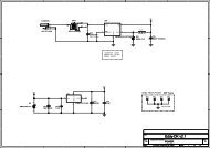
2.1.1 Power supply VCC<br />
It is necessary to provide a clean and stable power supply for our GPS module in order to obtain<br />
good performances. Unstable power source will have a significant negative impact on the GPS<br />
performance. To achieve this, the Vcc ripple must be controlled under 50mVpp. In addition, there are<br />
also some important suggestions for main power circuit design:<br />
(1). Add ferrite bead, power choke or low pass filter for power noise reduction<br />
(2). linear regulator is better than switch DC/DC power supplier in ripple<br />
(3). Use enough decoupling capacitors beside VCC for stable voltage.<br />
Power design for GPS module<br />
This document is the exclusive property of GlobalTop Tech Inc. and should not be distributed, reproduced, into any other format without<br />
prior permission of GlobalTop Tech Inc. Specifications subject to change without prior notice.<br />
Copyright © 2012 GlobalTop Technology Inc. All Rights Reserved.<br />
7
GlobalTop Technology<br />
GPS <strong>Module</strong> <strong>Application</strong> <strong>Note</strong>s (<strong>MT3339</strong> <strong>series</strong>)<br />
2.1.2 VBACKUP backup battery<br />
Compatible Mode: SL3C, Gmm-u2p, PA6C, PA6H, Gms-u6b<br />
There are 2 applications for applied VBACKUP to GPS module.<br />
<strong>Application</strong> 1:<br />
Ver. <strong>A00</strong><br />
Backup power is used for keeping RTC running and navigation data after the main power was turn<br />
off. For a short term VCC off, with backup power, the GPS module can have a faster TTFF, Time to<br />
First Fix, or hot start when next power on.<br />
It is recommended to connect the module VBACKUP to a sustained power source (ex: Li-Ion<br />
rechargeable coin battery, super cap) for backup power. See figure for reference.<br />
About super capacitor reference design, please refer to Appendix I: Super Capacitor Design.<br />
GPS module is already built-in a charge circuit for the battery charging function, it will charge battery<br />
while GPS module working and that will extend the battery life.<br />
<strong>Application</strong> 2:<br />
Using Coin Battery for GPS module<br />
Since GPS module already built-in a charging circuit that also supply the VBACKUP a available voltage,<br />
the module still work fine if a external coin battery for VBACKUP is not installed.<br />
Because VBACKUP power was not installed, the GPS module will perform a cold start every time it is<br />
powered on.<br />
This document is the exclusive property of GlobalTop Tech Inc. and should not be distributed, reproduced, into any other format without<br />
prior permission of GlobalTop Tech Inc. Specifications subject to change without prior notice.<br />
Copyright © 2012 GlobalTop Technology Inc. All Rights Reserved.<br />
8
GlobalTop Technology<br />
GPS <strong>Module</strong> <strong>Application</strong> <strong>Note</strong>s (<strong>MT3339</strong> <strong>series</strong>)<br />
Built-in a charging circuit for GPS module<br />
Ver. <strong>A00</strong><br />
This document is the exclusive property of GlobalTop Tech Inc. and should not be distributed, reproduced, into any other format without<br />
prior permission of GlobalTop Tech Inc. Specifications subject to change without prior notice.<br />
Copyright © 2012 GlobalTop Technology Inc. All Rights Reserved.<br />
9
GlobalTop Technology<br />
GPS <strong>Module</strong> <strong>Application</strong> <strong>Note</strong>s (<strong>MT3339</strong> <strong>series</strong>)<br />
2.1.3 UART 0 (RX/TX) –Serial Interface<br />
Compatible Mode: SL3C, Gmm-u2p, PA6C, PA6H, Gms-u6b<br />
Ver. <strong>A00</strong><br />
(1). UART is the default interface (TTL level) that has the baud rate ranging from 4800 bps to 115200<br />
bps.<br />
(2). Placing damping resistor on the RX and TX of the GPS module could limit the interference from<br />
host MCU or high speed digital logics. Fine tuning the damping resistor is required to suppress<br />
interference efficient. The damping resistor would be a chock coil as well.<br />
(3). Please leave RX open if it is not used as there is an internal pull-up to VCC.<br />
(4). Please don’t connect diode(s) to RX/TX as it will decrease signal driving capability which might<br />
adversely affect RX/TX signal level (ex. no data output).<br />
(5). If RS232 logic-level is needed for any particular application, and then the level shifter is<br />
necessary. Please refer to “Appendix III: UART to RS232 Interface” for more information.<br />
(6). If USB logic-level is needed for any particular application. Please refer to “Appendix IV: UART to<br />
USB Interface” for more information.<br />
2.1.4 GND-Ground<br />
Compatible Mode: SL3C, Gmm-u2p, PA6C, PA6H, Gms-u6b<br />
Make sure all GND pins of module are connected to a good ground plane.<br />
Please refer to “2.2.5 Ground Segmentation”.<br />
This document is the exclusive property of GlobalTop Tech Inc. and should not be distributed, reproduced, into any other format without<br />
prior permission of GlobalTop Tech Inc. Specifications subject to change without prior notice.<br />
Copyright © 2012 GlobalTop Technology Inc. All Rights Reserved.<br />
10
GlobalTop Technology<br />
GPS <strong>Module</strong> <strong>Application</strong> <strong>Note</strong>s (<strong>MT3339</strong> <strong>series</strong>)<br />
2.1.5 Antenna Compliance Design<br />
Compatible Mode: SL3C, Gmm-u2p, PA6H,<br />
GPS antenna is a receiving device to acquire weak GPS signal from sky. Popular solution would be<br />
ceramic patch antenna because of its small form factor with low cost. There are two types of<br />
antennas, passive and active.<br />
Passive antenna is with solely antenna itself such as Patch Antenna and Chip Antenna.<br />
Ver. <strong>A00</strong><br />
External antenna is a stand long device integrates with LNA, Patch Antenna and Cable to have high<br />
gain and good performance.<br />
Antenna can be chosen according to radiation efficiency, radiation pattern, gain, bandwidth, form<br />
factor and cost. Make sure the ground plane is sufficient for the antenna to operate with good<br />
enough performance.<br />
Design Patch antenna with GPS module.<br />
(1). Generally speaking, a 50Ω Patch antenna will work good with GPS module just connect the<br />
Antenna_IN with a 50Ω impedance trace.<br />
(2). please refer to “Appendix II: About 50 Ω Matching Line “for PCB impedance design”.<br />
(3). Pls keep the Patch antenna far away noise source such as switch power supplier and high speed<br />
digital logics.<br />
(4). The 50Ω trace should keep as short as possible to reduce the chance to receive the noise from<br />
air and PCB. A simple direct line is recommended.<br />
(5). If need, a match circuit could be place between Patch antenna and GPS module. The match<br />
circuit should be discussed with module and Patch Antenna maker by case.<br />
Antenna design for module<br />
This document is the exclusive property of GlobalTop Tech Inc. and should not be distributed, reproduced, into any other format without<br />
prior permission of GlobalTop Tech Inc. Specifications subject to change without prior notice.<br />
Copyright © 2012 GlobalTop Technology Inc. All Rights Reserved.<br />
11
GlobalTop Technology<br />
GPS <strong>Module</strong> <strong>Application</strong> <strong>Note</strong>s (<strong>MT3339</strong> <strong>series</strong>)<br />
Select External Antennal architecture with GPS module.<br />
For an external antenna, it needs a DC power to have it work properly.<br />
A typical method is to feed a DC into the RF trace and the External Antenna can extract the DC<br />
from RF trace. Thus we can use the RF trace to transport both RF signal and DC volt.<br />
We use a RF chock coil to couple the DC to RF trace to perform the mentioned method.<br />
In GTOP module, we applied 3 kinds of architectures in our related module.<br />
Please customer select the module carefully while applying the design with an External Antenna.<br />
Ver. <strong>A00</strong><br />
• Mode1 (ex. SL3C), the power supply for the External Antenna needs to be externally feed<br />
into pin VANT of the module and connect to Antenna_IN via a internal chock coil.<br />
• Mode2 (ex. Gmm-u2p), the power supply needs to be externally provided and is connected<br />
directly to the External Antenna via chock coil.<br />
<strong>Note</strong>: Chock Coil for reference: LQG15HS33NJ02D (Murata)<br />
• Mode3 (ex.PA6H), the power supply comes from VCC via an antenna supervise circuit to<br />
monitor the status of DC current and limit the supplied current (over current protection).<br />
Typically, the current is limited if current >30mA.<br />
The circuit also auto switch RF signal from internal Patch Antenna to External Antenna when<br />
connect an External Antenna.<br />
Mode<br />
Model 1<br />
<strong>Module</strong><br />
(Internal chock coil) <br />
Model 2<br />
(External chock coil)<br />
Model 3<br />
(built-in Antenna<br />
Supervisor)<br />
SL3C Gmm-u2p PA6H<br />
This document is the exclusive property of GlobalTop Tech Inc. and should not be distributed, reproduced, into any other format without<br />
prior permission of GlobalTop Tech Inc. Specifications subject to change without prior notice.<br />
Copyright © 2012 GlobalTop Technology Inc. All Rights Reserved.<br />
<br />
<br />
12
GlobalTop Technology<br />
GPS <strong>Module</strong> <strong>Application</strong> <strong>Note</strong>s (<strong>MT3339</strong> <strong>series</strong>)<br />
Model 1 Model 2<br />
Model 3<br />
Ver. <strong>A00</strong><br />
This document is the exclusive property of GlobalTop Tech Inc. and should not be distributed, reproduced, into any other format without<br />
prior permission of GlobalTop Tech Inc. Specifications subject to change without prior notice.<br />
Copyright © 2012 GlobalTop Technology Inc. All Rights Reserved.<br />
13
GlobalTop Technology<br />
GPS <strong>Module</strong> <strong>Application</strong> <strong>Note</strong>s (<strong>MT3339</strong> <strong>series</strong>)<br />
2.1.6 1PPS<br />
Compatible Mode: SL3C, Gmm-u2p, PA6C, PA6H, Gms-u6b<br />
1PPS signal is an output pulse signal used for timing application, its electronic characteristic are<br />
listed below:<br />
1PPS signal and its pulse width with 100ms duration<br />
Low Voltage level: 0~0.4V<br />
High Voltage level: 2.8~3.1V<br />
Duration: 100ms (Firmware customization for duration is available)<br />
Period: 1s<br />
Accuracy (jitter):10ns<br />
Ver. <strong>A00</strong><br />
Free run 1PPS output before 3D_FIX<br />
Standard GPS module will output the 1pps after the module is 3D_FIX.<br />
A customize firmware could set the 1PPS plus out as soon as power-on disregard to 3D_Fix or not.<br />
Please be noted that the accuracy before 3D_Fix on the 1PPS is a free run plus and will real lock until<br />
GPS 3D_Fix.<br />
Cable delay compensation<br />
For a timing application, it could be connected to a cable for a long distance connection (~300m).<br />
Please refer to Appendix V for more information on 1PPS signal transmission delay.<br />
Please also be noted that the delay caused by the cable could be compensated with firmware setting.<br />
Please contact us if that is useful for customer.<br />
This document is the exclusive property of GlobalTop Tech Inc. and should not be distributed, reproduced, into any other format without<br />
prior permission of GlobalTop Tech Inc. Specifications subject to change without prior notice.<br />
Copyright © 2012 GlobalTop Technology Inc. All Rights Reserved.<br />
14
GlobalTop Technology<br />
GPS <strong>Module</strong> <strong>Application</strong> <strong>Note</strong>s (<strong>MT3339</strong> <strong>series</strong>)<br />
LED indicator for 1PPS<br />
Customer can also connect a LED with a 330 Ω to GND for the indication of specific indicator.<br />
1PPS signal design for IO<br />
2.1.7 3D_Fix<br />
Compatible Mode: SL3C, Gmm-u2p, PA6C, PA6H, Gms-u6b<br />
3D_Fix signal is an output pulse signal used for GPS fix application, its electronic characteristic are<br />
listed below:<br />
Ver. <strong>A00</strong><br />
This document is the exclusive property of GlobalTop Tech Inc. and should not be distributed, reproduced, into any other format without<br />
prior permission of GlobalTop Tech Inc. Specifications subject to change without prior notice.<br />
Copyright © 2012 GlobalTop Technology Inc. All Rights Reserved.<br />
15
GlobalTop Technology<br />
GPS <strong>Module</strong> <strong>Application</strong> <strong>Note</strong>s (<strong>MT3339</strong> <strong>series</strong>)<br />
Low Voltage level: 0~0.4V<br />
High Voltage level: 2.8~3.1V<br />
Source current: 14 mA, Sink current 14 mA<br />
Before 2D Fix:<br />
Duration: High level with one-second and Low level with one-second<br />
Period: 2s<br />
(Firmware customization for duration is available)<br />
After 2D or 3D Fix:<br />
Duration: Continuously output low-level<br />
(Firmware customization for duration is available)<br />
Customer can also connect a LED with a 330Ω to GND for the indication.<br />
Ver. <strong>A00</strong><br />
This document is the exclusive property of GlobalTop Tech Inc. and should not be distributed, reproduced, into any other format without<br />
prior permission of GlobalTop Tech Inc. Specifications subject to change without prior notice.<br />
Copyright © 2012 GlobalTop Technology Inc. All Rights Reserved.<br />
16
GlobalTop Technology<br />
GPS <strong>Module</strong> <strong>Application</strong> <strong>Note</strong>s (<strong>MT3339</strong> <strong>series</strong>)<br />
3D_Fix signal design for IO<br />
<strong>Note</strong>: Please do not connect a LED with 330Ωfrom VCC .<br />
That will cause an internal function fail of GPS module.<br />
NG<br />
Ver. <strong>A00</strong><br />
This document is the exclusive property of GlobalTop Tech Inc. and should not be distributed, reproduced, into any other format without<br />
prior permission of GlobalTop Tech Inc. Specifications subject to change without prior notice.<br />
Copyright © 2012 GlobalTop Technology Inc. All Rights Reserved.<br />
17
GlobalTop Technology<br />
GPS <strong>Module</strong> <strong>Application</strong> <strong>Note</strong>s (<strong>MT3339</strong> <strong>series</strong>)<br />
2.2 Layout Guideline<br />
Please follow the layout criteria to design a system using GPS module.<br />
2.2.1 Layout underneath the GPS module<br />
Compatible Mode: SL3C, Gmm-u2p, PA6C, PA6H, Gms-u6b<br />
Ver. <strong>A00</strong><br />
GPS signal is very weak signal level around -160dBm~130dBm. Any noise or harmonic will<br />
decrease the quality of GPS. In modern GPS product, it almost includes LCD, MCU, High<br />
Speed digital and RF system (BT, Wi-Fi, DVB-T…). In order to minimize the influence of<br />
mentioned noise to GPS module, please customer don’t place any trace underneath the GPS<br />
module. In other word, give GPS module a clean GND plane is very important.<br />
GPS on a clean GND plane<br />
For module PA6H and PA6C, place a hold according to the location of RF feeding pin in<br />
module. The hole will keep the RF feeding pin far away customer’s GND plane that will<br />
minimize the loss caused by the coupling of antenna signal to GND.<br />
This document is the exclusive property of GlobalTop Tech Inc. and should not be distributed, reproduced, into any other format without<br />
prior permission of GlobalTop Tech Inc. Specifications subject to change without prior notice.<br />
Copyright © 2012 GlobalTop Technology Inc. All Rights Reserved.<br />
18
GlobalTop Technology<br />
GPS <strong>Module</strong> <strong>Application</strong> <strong>Note</strong>s (<strong>MT3339</strong> <strong>series</strong>)<br />
GPS on a clean GND plane and antenna hole<br />
Ver. <strong>A00</strong><br />
This document is the exclusive property of GlobalTop Tech Inc. and should not be distributed, reproduced, into any other format without<br />
prior permission of GlobalTop Tech Inc. Specifications subject to change without prior notice.<br />
Copyright © 2012 GlobalTop Technology Inc. All Rights Reserved.<br />
19
GlobalTop Technology<br />
GPS <strong>Module</strong> <strong>Application</strong> <strong>Note</strong>s (<strong>MT3339</strong> <strong>series</strong>)<br />
2.2.2 Keep far away from high profile or metal canned components<br />
Compatible Mode: PA6C, PA6H, Gms-u6b<br />
Ver. <strong>A00</strong><br />
For PA6C, PA6H, It is better to place GPS module far away a high profile component especially with<br />
metal case enclosed products such as E-CAP. That will cause the distortion of the Antenna field<br />
pattern and the worst case will decrease the GPS signal up to ~10dB.<br />
2.2.3 Placement<br />
Compatible Mode: SL3C, Gmm-u2p, PA6C, PA6H, Gms-u6b<br />
Place the decoupling capacitors close to GPS module<br />
Place the damping resistors close to GPS module<br />
Do not place:<br />
GPS module close to high-speed digital processing circuitry<br />
GPS module close to high-current switching power circuitry<br />
GPS module close to clock sources circuitry<br />
Patch Antenna close to the high profile metal case component as 2.2.2 said.<br />
This document is the exclusive property of GlobalTop Tech Inc. and should not be distributed, reproduced, into any other format without<br />
prior permission of GlobalTop Tech Inc. Specifications subject to change without prior notice.<br />
Copyright © 2012 GlobalTop Technology Inc. All Rights Reserved.<br />
20
GlobalTop Technology<br />
GPS <strong>Module</strong> <strong>Application</strong> <strong>Note</strong>s (<strong>MT3339</strong> <strong>series</strong>)<br />
2.2.4 Trace<br />
Compatible Mode: SL3C, Gmm-u2p, PA6C, PA6H, Gms-u6b<br />
Ver. <strong>A00</strong><br />
(1). The USB differential signals should be trace close and equal-length for minimum radiation and<br />
noise immunity.<br />
(2). Please have the RF traces had the character impendence of 50 ohm for good impedance<br />
matching.<br />
(3). Any right angle turn in trace routing should be accomplished with two 135 degree turn or an arc<br />
turn<br />
It is better to have independent trace of power source for any device<br />
This document is the exclusive property of GlobalTop Tech Inc. and should not be distributed, reproduced, into any other format without<br />
prior permission of GlobalTop Tech Inc. Specifications subject to change without prior notice.<br />
Copyright © 2012 GlobalTop Technology Inc. All Rights Reserved.<br />
21
GlobalTop Technology<br />
GPS <strong>Module</strong> <strong>Application</strong> <strong>Note</strong>s (<strong>MT3339</strong> <strong>series</strong>)<br />
2.2.5 Ground Segmentation<br />
Compatible Mode: SL3C, Gmm-u2p, PA6C, PA6H, Gms-u6b<br />
Ver. <strong>A00</strong><br />
The separation of ground between GPS module and the rest of the system is recommended to avoid<br />
interference. If this is not possible, it is best to follow these typical rules: segmentation of ground<br />
between digital and analogue system, high current and low current system, and different radiation<br />
systems in general (such as GPS and GPRS).<br />
One way to segment the ground is to place digital and noise component at one corner of the board,<br />
while placing analog and quiet components at the opposite corner of the board. Make sure there is<br />
no crossing of microstrip or current between the two component sets and grounds of each sets are<br />
contacted in one point only.<br />
Another way to do this is the place the two different sets at different layers of the board, while the<br />
ground of each layer is contacted in one point only (preferable at border of the board).<br />
2.2.6 Ground Plane<br />
Compatible Mode: PA6C, PA6H, Gms-u6b<br />
For PA6C and PA6H, a large GND plane direct underneath the module could enhance the magneticfield<br />
line of the antenna for better GPS signal reception. Typical it will improve ~2dB as maximum.<br />
It is strongly recommended to have a ground plane designed underneath the GPS module as big as<br />
possible.<br />
The recommended thickness for the ground layer is 0.5 to 1 OZ (0.0175 to 0.035 mm)<br />
It is best to place the ground plane on the top layer of the PCB, directly underneath the GPS module<br />
as the figure below shows:<br />
This document is the exclusive property of GlobalTop Tech Inc. and should not be distributed, reproduced, into any other format without<br />
prior permission of GlobalTop Tech Inc. Specifications subject to change without prior notice.<br />
Copyright © 2012 GlobalTop Technology Inc. All Rights Reserved.<br />
22
GlobalTop Technology<br />
GPS <strong>Module</strong> <strong>Application</strong> <strong>Note</strong>s (<strong>MT3339</strong> <strong>series</strong>)<br />
Ground Plane for FR4 Design<br />
For module Gms-u6b, built-in Chip Antenna, a special ground plane is required for chip antenna<br />
reception performance improvement.<br />
As shown in the figure, the area circled according to the antenna area of module should be kept<br />
Ground-Clarence all layers.<br />
Ver. <strong>A00</strong><br />
This document is the exclusive property of GlobalTop Tech Inc. and should not be distributed, reproduced, into any other format without<br />
prior permission of GlobalTop Tech Inc. Specifications subject to change without prior notice.<br />
Copyright © 2012 GlobalTop Technology Inc. All Rights Reserved.<br />
23
GlobalTop Technology<br />
GPS <strong>Module</strong> <strong>Application</strong> <strong>Note</strong>s (<strong>MT3339</strong> <strong>series</strong>)<br />
3. Thermal Profile for SMD <strong>Module</strong>s<br />
(Reference Only)<br />
Ver. <strong>A00</strong><br />
*All the information in this sheet should be used only for Pb-free<br />
certification.<br />
SMT Reflow Soldering Temperature Profile:<br />
Average ramp-up rate (25 ~ 150°C): 3°C/sec. max.<br />
Average ramp-up rate (270°C to peak): 3°C/sec. max.<br />
Preheat: 175 ± 25°C 、60 ~ 120 seconds<br />
Temperature maintained above 217°C: 60~150 seconds<br />
Peak temperature: 250 +0/-5°C、20~40 seconds<br />
Ramp-down rate: 6°C/sec. max.<br />
Time 25°C to peak temperature: 8 minutes max.<br />
SMT Solder Mask:<br />
Please use the dimension of PCB pad as reference and shrink the size by 0.1 to 0.2 mm and use that<br />
as layout for paste mask. (For PCB pad layout, please see “Recommended PCB pad layout” on<br />
individual GPS module data sheet)<br />
Manual Soldering:<br />
Soldering iron: Bit Temperature: Under 380°C Time: Under 3 second.<br />
This document is the exclusive property of GlobalTop Tech Inc. and should not be distributed, reproduced, into any other format without<br />
prior permission of GlobalTop Tech Inc. Specifications subject to change without prior notice.<br />
Copyright © 2012 GlobalTop Technology Inc. All Rights Reserved.<br />
24
GlobalTop Technology<br />
GPS <strong>Module</strong> <strong>Application</strong> <strong>Note</strong>s (<strong>MT3339</strong> <strong>series</strong>)<br />
4. Troubleshooting<br />
How to check for the working status of GPS module?<br />
Ver. <strong>A00</strong><br />
The first thing to check for is the NMEA sentence output through TX by using various application<br />
tools. For example: you can use windows default tool - WinXP Hyperterminal, or you can use other<br />
GPS application program to check for GPS status.<br />
If there is no NMEA output, this indicates the module is currently not working. Please double check<br />
your schematic design. Down below we listed some of the possible items to check for your reference:<br />
Item 1: VCC<br />
The voltage should be kept between 3V to 4.3V. (Typical:3.3V), Please double-check.<br />
Item 2: VBACKUP<br />
The voltage should be kept between 2.0V~4.3V. (Typical:3.0V). If the module has no battery for<br />
the VBACKUP, the pin still could be measure a voltage by built-in charge circuit. It is recommended<br />
that a sustain power for VBACUP is supplied to keep RTC time and navigation data, Please doublecheck<br />
Item 3: 3D-FIX<br />
If all the measurements are within the specifications, please also measure 3D-FIX signal. Before 2D<br />
Fix, the pin should output one-second high-level signal follow with one-second low-level signal.<br />
Item 4: TX0<br />
The UART transmitter of the module, it outputs the GPS NMEA information for application.<br />
This document is the exclusive property of GlobalTop Tech Inc. and should not be distributed, reproduced, into any other format without<br />
prior permission of GlobalTop Tech Inc. Specifications subject to change without prior notice.<br />
Copyright © 2012 GlobalTop Technology Inc. All Rights Reserved.<br />
25
GlobalTop Technology<br />
GPS <strong>Module</strong> <strong>Application</strong> <strong>Note</strong>s (<strong>MT3339</strong> <strong>series</strong>)<br />
Ver. <strong>A00</strong><br />
This document is the exclusive property of GlobalTop Tech Inc. and should not be distributed, reproduced, into any other format without<br />
prior permission of GlobalTop Tech Inc. Specifications subject to change without prior notice.<br />
Copyright © 2012 GlobalTop Technology Inc. All Rights Reserved.<br />
26
GlobalTop Technology<br />
GPS <strong>Module</strong> <strong>Application</strong> <strong>Note</strong>s (<strong>MT3339</strong> <strong>series</strong>)<br />
5. Contact<br />
For help or further information, please contact us via the following methods:<br />
GlobalTop Technology Inc.<br />
Tainan Science-Based Industry Park Headquarter:<br />
Address: No.16 Nan-ke 9th Road Science-based Industrial Park, Tainan 74147,<br />
Taiwan<br />
Tel: +886-6-505-1268<br />
Fax: +886-6-505-3381<br />
Sales Email: sales@gtop-tech.com<br />
Technical Support Email: support@gtop-tech.com<br />
Ver. <strong>A00</strong><br />
This document is the exclusive property of GlobalTop Tech Inc. and should not be distributed, reproduced, into any other format without<br />
prior permission of GlobalTop Tech Inc. Specifications subject to change without prior notice.<br />
Copyright © 2012 GlobalTop Technology Inc. All Rights Reserved.<br />
27
GlobalTop Technology<br />
GPS <strong>Module</strong> <strong>Application</strong> <strong>Note</strong>s (<strong>MT3339</strong> <strong>series</strong>)<br />
Appendix I: Super Capacitor Design<br />
About Super Capacitors<br />
Super capacitors have a useful life-time similar to aluminum electrolytic capacitors. The life of a<br />
super capacitors capacitor is largely dependent on the operating temperature, humidity, applied<br />
voltage, current and backup time requirements. Therefore, the life of a super capacitor is<br />
determined based on the backup time set by the customer.<br />
How to calculate the backup time<br />
The example below teaches how to calculate the backup time.<br />
Ver. <strong>A00</strong><br />
This document is the exclusive property of GlobalTop Tech Inc. and should not be distributed, reproduced, into any other format without<br />
prior permission of GlobalTop Tech Inc. Specifications subject to change without prior notice.<br />
Copyright © 2012 GlobalTop Technology Inc. All Rights Reserved.<br />
28
GlobalTop Technology<br />
GPS <strong>Module</strong> <strong>Application</strong> <strong>Note</strong>s (<strong>MT3339</strong> <strong>series</strong>)<br />
Appendix II: About 50 Ω Matching Line<br />
We used AppCAD tool for 50 Ω impedance calculation of RF line and made a table for layout<br />
reference.<br />
Notice:<br />
RF line width<br />
(W)<br />
PCB FR4<br />
Thickness<br />
(H)<br />
Dielectric<br />
parameter<br />
Copper<br />
Thickness<br />
an ounce<br />
1.8mm 1mm 4.6 0.035mm<br />
Ver. <strong>A00</strong><br />
For multiple-layer layout, designer could place a ground layer in 2nd layer to minimize the<br />
trace width in specific PCB (such FR4) and impedance.<br />
For impedance calculation, free software to calculate trace width or impedance is available.<br />
Please refer to the website for one such software:<br />
http://web.awrcorp.com/Usa/Products/Optional-Products/TX-Line/<br />
This document is the exclusive property of GlobalTop Tech Inc. and should not be distributed, reproduced, into any other format without<br />
prior permission of GlobalTop Tech Inc. Specifications subject to change without prior notice.<br />
Copyright © 2012 GlobalTop Technology Inc. All Rights Reserved.<br />
29
GlobalTop Technology<br />
GPS <strong>Module</strong> <strong>Application</strong> <strong>Note</strong>s (<strong>MT3339</strong> <strong>series</strong>)<br />
Appendix III: UART to RS232 Interface<br />
Ver. <strong>A00</strong><br />
Typically RS232 or USB interface is required to connect GlobalTop GPS module directly to<br />
the PC for communication. Majority of GlobalTop modules uses a set of communication port<br />
in TTL-logic (and a newer ones have support for direct USB connection) and a bridge IC is<br />
needed for conversion to RS232 level.<br />
Please note the supported baud-rates are: 4800, 9600, 14400, 19200, 38400, 57600, and<br />
115200 bps.<br />
Please refer to the reference circuits below for such conversion: (using SP3320 IC as an<br />
example)<br />
This document is the exclusive property of GlobalTop Tech Inc. and should not be distributed, reproduced, into any other format without<br />
prior permission of GlobalTop Tech Inc. Specifications subject to change without prior notice.<br />
Copyright © 2012 GlobalTop Technology Inc. All Rights Reserved.<br />
30
GlobalTop Technology<br />
GPS <strong>Module</strong> <strong>Application</strong> <strong>Note</strong>s (<strong>MT3339</strong> <strong>series</strong>)<br />
Appendix IV: UART to USB Interface<br />
Ver. <strong>A00</strong><br />
If the GlobalTop module you have chosen does not contain USB interface or if you do not<br />
wish to use the integrated USB interface (perhaps due to driver or other concerns), it is<br />
possible to connect it to an external USB IC and further enhance the transferring speed by<br />
using a one capable of USB 2.0 interface. Once the driver for the chosen USB Bridge IC is<br />
successfully installed for Windows or other operating system, the USB Bridge IC will be<br />
automatically recognized as a com port within the operating system.<br />
<strong>Note</strong>: proper driver must be installed or else the operating system will not be able to<br />
recognize the device!<br />
Please refer to the reference circuits below for such conversion: (using CP2102 IC as an<br />
example)<br />
(The Pin29 and Pin30 are the bottom ground pads which not be listed in IC data sheet, customer<br />
could create the decal omitted this 2 pin)<br />
This document is the exclusive property of GlobalTop Tech Inc. and should not be distributed, reproduced, into any other format without<br />
prior permission of GlobalTop Tech Inc. Specifications subject to change without prior notice.<br />
Copyright © 2012 GlobalTop Technology Inc. All Rights Reserved.<br />
31
GlobalTop Technology<br />
GPS <strong>Module</strong> <strong>Application</strong> <strong>Note</strong>s (<strong>MT3339</strong> <strong>series</strong>)<br />
Appendix V: How to efficiently transfer 1PPS<br />
through extended distances<br />
Ver. <strong>A00</strong><br />
There are several things to watch out for when transferring 1PPS through long distances which will<br />
result in 1PPS signal degradation, noise and delays if proper attentions are not being paid. As the<br />
1PPS signal passes through the communication cable, matching resistance must be implemented to<br />
prevent wave form distortions. Depending on user’s application, OPA can be added to effectively<br />
control the accuracy of the voltage level determination for the 1PPS signal.<br />
When using 1PPS signal to synchronize time, the OPA chosen should have a high slew rate property<br />
to prevent large delay in the 1PPS. The accuracy level of 1PPS for GlobalTop GPS module is within<br />
100ns (same for majority of MTK GPS modules). The reference design below can help improving this<br />
accuracy to within 80ns.<br />
This document is the exclusive property of GlobalTop Tech Inc. and should not be distributed, reproduced, into any other format without<br />
prior permission of GlobalTop Tech Inc. Specifications subject to change without prior notice.<br />
Copyright © 2012 GlobalTop Technology Inc. All Rights Reserved.<br />
32
GlobalTop Technology<br />
GPS <strong>Module</strong> <strong>Application</strong> <strong>Note</strong>s (<strong>MT3339</strong> <strong>series</strong>)<br />
1PPS Delay Time:<br />
When using coaxial cable for long distances communication using OPA amplification, please pay<br />
close attention on the time delay caused by the coaxial cable and rising time of the wave form<br />
affected by OPA’s SR. A brief explanation for this is provided below:<br />
The model number for the coaxial cable is RG6U, where the figure below shows its specification.<br />
Ver. <strong>A00</strong><br />
This document is the exclusive property of GlobalTop Tech Inc. and should not be distributed, reproduced, into any other format without<br />
prior permission of GlobalTop Tech Inc. Specifications subject to change without prior notice.<br />
Copyright © 2012 GlobalTop Technology Inc. All Rights Reserved.<br />
33
GlobalTop Technology<br />
GPS <strong>Module</strong> <strong>Application</strong> <strong>Note</strong>s (<strong>MT3339</strong> <strong>series</strong>)<br />
The delay time cause by the cable:<br />
How to calculate the delay time of the communication cable with the length of “N”<br />
The simplest method to calculate this is to have a good grasp on the relationship between:<br />
1. The speed of the waveform<br />
2. The distance of the wave form traveled<br />
3. The delay time<br />
Distance of the wave form traveled (m)<br />
Speed of the waveform (m/s)<br />
Ver. <strong>A00</strong><br />
The waveform in the<br />
coaxial cable is travelling<br />
close to the speed of light,<br />
but will show significant<br />
delay as the cable<br />
becomes longer.<br />
This document is the exclusive property of GlobalTop Tech Inc. and should not be distributed, reproduced, into any other format without<br />
prior permission of GlobalTop Tech Inc. Specifications subject to change without prior notice.<br />
Copyright © 2012 GlobalTop Technology Inc. All Rights Reserved.<br />
34
GlobalTop Technology<br />
GPS <strong>Module</strong> <strong>Application</strong> <strong>Note</strong>s (<strong>MT3339</strong> <strong>series</strong>)<br />
Delay Time (ns)<br />
Ver. <strong>A00</strong><br />
If the speed of the waveform (in coaxial cable) is unknown, it is possible to use a short sip of coaxial<br />
cable to test for this. For example, the signal travelling in 1 meter of coaxial cable can have its delay<br />
time measured by the oscilloscope as 5ns, and consequently the will be 2 * 10 8 (m/s).<br />
If the value of resistance and inductance for the coaxial cable is known, then perhaps (m/s) can<br />
be calculated as well.<br />
Moreover, fundamentals of electromagnetics such as RLCG parameters for the coaxial cable<br />
(including resistance, inductance, capacitance, and conductance), together with the inner and outer<br />
diameter of the cable, can be used in combination to perform theoretical calculations.<br />
Waveform rising time caused by OPA<br />
Recommended OPA<br />
If inadequate OPA is chosen (with low slew rate), the delayed caused by waveform rising time will be<br />
significantly longer than the delay in time caused by the coaxial wire.<br />
We recommend using OPA301 to decrease the waveform rising time<br />
Specification of OPA301:<br />
The left figure shows Slew Rate:<br />
which is the time needed for<br />
rising waveform. When the SR<br />
(V/μsec) of OPA is higher, the<br />
rising time will be shortened as<br />
well.<br />
This document is the exclusive property of GlobalTop Tech Inc. and should not be distributed, reproduced, into any other format without<br />
prior permission of GlobalTop Tech Inc. Specifications subject to change without prior notice.<br />
Copyright © 2012 GlobalTop Technology Inc. All Rights Reserved.<br />
35
GlobalTop Technology<br />
GPS <strong>Module</strong> <strong>Application</strong> <strong>Note</strong>s (<strong>MT3339</strong> <strong>series</strong>)<br />
◎Low Power:9.5mA (Typ) on 5.5V<br />
◎Single Power:2.7V ~ 5.5V<br />
◎High Slew Rate:80 V/μsec<br />
◎Tiny Packages:MSOP and SOT23<br />
Voltage degradation of communication cable<br />
We have tested a 10m long coaxial cable and only insignificant amount of voltage degradation is<br />
observed. Users should not be concerned with this issue.<br />
Ver. <strong>A00</strong><br />
This document is the exclusive property of GlobalTop Tech Inc. and should not be distributed, reproduced, into any other format without<br />
prior permission of GlobalTop Tech Inc. Specifications subject to change without prior notice.<br />
Copyright © 2012 GlobalTop Technology Inc. All Rights Reserved.<br />
36
GlobalTop Technology<br />
GPS <strong>Module</strong> <strong>Application</strong> <strong>Note</strong>s (<strong>MT3339</strong> <strong>series</strong>)<br />
Ver. <strong>A00</strong><br />
Appendix VI: Cautions on Reflow Soldering Process<br />
Details Suggestions <strong>Note</strong>s<br />
1 Before proceeding with the reflowsoldering<br />
process, the GPS module must<br />
be pre-baked.<br />
2 Because PCBA (along with the patch<br />
antenna) is highly endothermic during<br />
the reflow-soldering process, extra care<br />
must be paid to the GPS module's solder<br />
joint to see if there are any signs of cold<br />
weld(ing) or false welding.<br />
3 Special attentions are needed for PCBA<br />
board during reflow-soldering to see if<br />
there are any symptoms of bending or<br />
deformation to the PCBA board,<br />
possibility due to the weight of the<br />
module. If so, this will cause concerns at<br />
the latter half of the production process.<br />
4 Before the PCBA is going through the<br />
reflow-soldering process, the production<br />
operators must check by eyesight to see<br />
if there are positional offset to the<br />
module, because it will be difficult to<br />
readjust after the module has gone<br />
through reflow-soldering process.<br />
Pre-bake Time:<br />
6 Hours @ 60°±5°C or<br />
4 Hours @ 70°±5°C<br />
The parameters of the<br />
reflow temperature<br />
must be set accordingly<br />
to module’s reflowsoldering<br />
temperature<br />
profile.<br />
A loading carrier fixture<br />
must be used with PCBA<br />
if the reflow soldering<br />
process is using rail<br />
conveyors for the<br />
production.<br />
The operators must<br />
check by eyesight and<br />
readjust the position<br />
before reflow-soldering<br />
process.<br />
The maximum tolerated<br />
temperature for the tray is<br />
100°C.<br />
After the pre-baking process,<br />
please make sure the<br />
temperature is sufficiently<br />
cooled down to 35°C or below in<br />
order to prevent any tray<br />
deformation.<br />
This document is the exclusive property of GlobalTop Tech Inc. and should not be distributed, reproduced, into any other format without<br />
prior permission of GlobalTop Tech Inc. Specifications subject to change without prior notice.<br />
Copyright © 2012 GlobalTop Technology Inc. All Rights Reserved.<br />
37<br />
Double check to see if the<br />
surrounding components around<br />
the GPS module are displaying<br />
symptoms of cold weld(ing) or<br />
false welding.<br />
If there is any bending or<br />
deformation to the PCBA board,<br />
this might causes the PCBA to<br />
collide into one another during<br />
the unloading process.<br />
If the operator is planning to<br />
readjust the module position,<br />
please do not touch the patch<br />
antenna while the module is hot<br />
in order to prevent rotational<br />
offset between the patch<br />
antenna and module
GlobalTop Technology<br />
GPS <strong>Module</strong> <strong>Application</strong> <strong>Note</strong>s (<strong>MT3339</strong> <strong>series</strong>)<br />
<strong>Note</strong>: References to patch antenna is referred to GPS modules with integrated Patch-on-top<br />
antennas (PA/Gms <strong>Module</strong> Series), and may not be applicable to all GPS modules.<br />
Details Suggestions <strong>Note</strong>s<br />
5 Before handling the PCBA, they must be<br />
cooled to 35°C or below after they have<br />
gone through the reflow-soldering<br />
process, in order to prevent positional<br />
shift that might occur when the module is<br />
still hot.<br />
6 1. When separating the PCBA panel into<br />
individual pieces using the V-Cut process,<br />
special attentions are needed to ensure<br />
there are sufficient gap between patch<br />
antennas so the patch antennas are not<br />
in contact with one another.<br />
2. If V-Cut process is not available and the<br />
pieces must be separated manually,<br />
please make sure the operators are not<br />
using excess force which may cause<br />
rotational offset to the patch antennas.<br />
7 When separating panel into individual<br />
pieces during latter half of the production<br />
process, special attentions are needed to<br />
ensure the patch antennas do not come<br />
in contact with one another in order to<br />
prevent chipped corners or positional<br />
shifts.<br />
1. Can use electric fans<br />
behind the Reflow<br />
machine to cool them<br />
down.<br />
2. Cooling the PCBA can<br />
prevent the module<br />
from shifting due to<br />
fluid effect.<br />
1. The blade and the<br />
patch antenna must<br />
have a distance gap<br />
greater than 0.6mm.<br />
2. Do not use patch<br />
antenna as the leverage<br />
point when separating<br />
the panels by hand.<br />
Use tray to separate<br />
individual pieces.<br />
Ver. <strong>A00</strong><br />
It is very easy to cause positional<br />
offset to the module and its<br />
patch antenna when handling<br />
the PCBA under high<br />
temperature.<br />
1. Test must be performed first<br />
to determine if V-Cut process is<br />
going to be used. There must be<br />
enough space to ensure the<br />
blade and patch antenna do not<br />
touch one another.<br />
2. An uneven amount of manual<br />
force applied to the separation<br />
will likely to cause positional<br />
shift in patch antenna and<br />
module.<br />
This document is the exclusive property of GlobalTop Tech Inc. and should not be distributed, reproduced, into any other format without<br />
prior permission of GlobalTop Tech Inc. Specifications subject to change without prior notice.<br />
Copyright © 2012 GlobalTop Technology Inc. All Rights Reserved.<br />
38<br />
It is possible to chip corner<br />
and/or cause a shift in position if<br />
patch antennas come in contact<br />
with each other.<br />
<strong>Note</strong>: References to patch antenna is referred to GPS modules with integrated Patch-on-top<br />
antennas (PA/Gms <strong>Module</strong> Series), and may not be applicable to all GPS modules.
GlobalTop Technology<br />
GPS <strong>Module</strong> <strong>Application</strong> <strong>Note</strong>s (<strong>MT3339</strong> <strong>series</strong>)<br />
Other Cautionary <strong>Note</strong>s on Reflow-Soldering Process:<br />
1. <strong>Module</strong> must be pre-baked before going through SMT solder reflow process.<br />
2. The usage of solder paste should follow “first in first out” principle. Opened solder paste<br />
needs to be monitored and recorded in a timely fashion (can refer to IPQC for related<br />
documentation and examples).<br />
Ver. <strong>A00</strong><br />
3. Temperature and humidity must be controlled in SMT production line and storage area.<br />
Temperature of 23°C, 60±5% RH humidity is recommended. (please refer to IPQC for related<br />
documentation and examples)<br />
4. When performing solder paste printing, please notice if the amount of solder paste is in<br />
excess or insufficient, as both conditions may lead to defects such as electrical shortage,<br />
empty solder and etc.<br />
5. Make sure the vacuum mouthpiece is able to bear the weight of the GPS module to prevent<br />
positional shift during the loading process.<br />
6. Before the PCBA is going through the reflow-soldering process, the operators should check<br />
by eyesight to see if there are positional offset to the module.<br />
7. The reflow temperature and its profile data must be measured before the SMT process and<br />
match the levels and guidelines set by IPQC.<br />
8. If SMT protection line is running a double-sided process for PCBA, please process GPS<br />
module during the second pass only to avoid repeated reflow exposures of the GPS module.<br />
Please contact GlobalTop beforehand if you must process GPS module during the 1 st pass of<br />
double-side process.<br />
Figure 6.2: Place GPS module right-side up when running reflow-solder process, do not invert.<br />
This document is the exclusive property of GlobalTop Tech Inc. and should not be distributed, reproduced, into any other format without<br />
prior permission of GlobalTop Tech Inc. Specifications subject to change without prior notice.<br />
Copyright © 2012 GlobalTop Technology Inc. All Rights Reserved.<br />
39
GlobalTop Technology<br />
GPS <strong>Module</strong> <strong>Application</strong> <strong>Note</strong>s (<strong>MT3339</strong> <strong>series</strong>)<br />
9. <strong>Module</strong> must be pre-baked before going through SMT solder reflow process.<br />
10. The usage of solder paste should follow “first in first out” principle. Opened solder paste<br />
needs to be monitored and recorded in a timely fashion (can refer to IPQC for related<br />
documentation and examples).<br />
Ver. <strong>A00</strong><br />
11. Temperature and humidity must be controlled in SMT production line and storage area.<br />
Temperature of 23°C, 60±5% RH humidity is recommended. (please refer to IPQC for related<br />
documentation and examples)<br />
12. When performing solder paste printing, please notice if the amount of solder paste is in<br />
excess or insufficient, as both conditions may lead to defects such as electrical shortage,<br />
empty solder and etc.<br />
13. The reflow temperature and its profile data must be measured before the SMT process and<br />
match the levels and guidelines set by IPQC.<br />
Manual Soldering<br />
Soldering iron:<br />
Bit Temperature: Under 380°C Time: Under 3 sec.<br />
<strong>Note</strong>s:<br />
1. Please do not directly touch the soldering pads on the surface of the PCB board, in order to<br />
prevent further oxidation<br />
2. The solder paste must be defrosted to room temperature before use so it can return to its<br />
optimal working temperature. The time required for this procedure is unique and dependent<br />
on the properties of the solder paste used.<br />
3. The steel plate must be properly assessed before and after use, so its measurement stays<br />
strictly within the specification set by SOP.<br />
4. Please watch out for the spacing between soldering joint, as excess solder may cause<br />
electrical shortage<br />
5. Please exercise with caution and do not use extensive amount of flux due to possible siphon<br />
effects on neighboring components, which may lead to electrical shortage.<br />
6. Please do not use the heat gun for long periods of time when removing the shielding or<br />
inner components of the GPS module, as it is very likely to cause a shift to the inner<br />
components and will leads to electrical shortage.<br />
This document is the exclusive property of GlobalTop Tech Inc. and should not be distributed, reproduced, into any other format without<br />
prior permission of GlobalTop Tech Inc. Specifications subject to change without prior notice.<br />
Copyright © 2012 GlobalTop Technology Inc. All Rights Reserved.<br />
40