U6808B - Adronic Components GmbH
U6808B - Adronic Components GmbH
U6808B - Adronic Components GmbH

You also want an ePaper? Increase the reach of your titles
YUMPU automatically turns print PDFs into web optimized ePapers that Google loves.
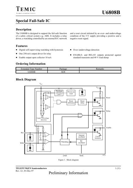
Special Fail-Safe IC<br />
Description<br />
The <strong>U6808B</strong> is designed to support the fail-safe function<br />
of a safety critical system e.g. ABS. It includes a relay<br />
driver, a watchdog controlled by an external R/C-network<br />
Features<br />
� Digital self-supervising watchdog with hysteresis<br />
� One 250-mA output driver for relay<br />
� Enable output open collector 10 mA<br />
Ordering Information<br />
TELEFUNKEN Semiconductors<br />
Rev. A1, 03-Dec-97<br />
Preliminary Information<br />
<strong>U6808B</strong><br />
and a reset circuit initiated by an over- and undervoltage<br />
condition of the 5-V supply providing a positive and a<br />
negative reset signal.<br />
� Over-/undervoltage detection<br />
� ENABLE- and RELAY outputs protected against<br />
standard transients and 40 V load dump<br />
Extended Type Number Package Remarks<br />
<strong>U6808B</strong> SO8<br />
Block Diagram<br />
Rin<br />
WDI<br />
V CC<br />
+<br />
–<br />
+<br />
–<br />
Under/ overvoltage<br />
detection<br />
–<br />
+<br />
+<br />
–<br />
Bandgap<br />
reference<br />
2.44 V<br />
Watchdog<br />
GND<br />
Power-on<br />
reset<br />
Reset<br />
debounce<br />
Figure 1. Block diagram<br />
Reset<br />
delay<br />
Internal<br />
oscillator<br />
RC<br />
oscillator<br />
WDC<br />
V CC<br />
Current<br />
limitation<br />
14523<br />
Reset<br />
Relay<br />
Enable<br />
1 (11)
<strong>U6808B</strong><br />
Pin Description<br />
Table 1. Pin description<br />
2 (11)<br />
RELAY<br />
GND<br />
ENABLE<br />
WDC<br />
1<br />
2<br />
3<br />
4<br />
Preliminary Information<br />
8<br />
7<br />
6<br />
5<br />
Figure 2. Pinning <strong>U6808B</strong><br />
VS<br />
RIN<br />
WDI<br />
RESET<br />
Pin Name Type Function Logic<br />
1 ÁÁÁÁÁÁ<br />
ÁÁÁÁÁÁ<br />
ÁÁÁÁÁÁ<br />
RELAY ÁÁÁÁÁÁÁ<br />
ÁÁÁÁÁÁÁÁ<br />
ÁÁÁÁÁÁÁÁÁÁÁÁ<br />
ÁÁÁÁÁÁÁ<br />
ÁÁÁÁÁÁÁÁ<br />
ÁÁÁÁÁÁÁÁÁÁÁÁ<br />
ÁÁÁÁÁÁÁÁÁÁÁÁ ÁÁÁÁÁÁÁÁ<br />
ÁÁÁÁÁÁ ÁÁÁÁÁÁÁ ÁÁÁÁÁÁÁÁÁÁÁÁ<br />
ÁÁÁÁÁÁÁÁ<br />
ÁÁÁÁÁÁÁ ÁÁÁÁÁÁÁÁÁÁÁÁ<br />
ÁÁÁÁÁÁ<br />
Open collector Fail-safe relay driver<br />
Driver off:–––<br />
driver output<br />
driver on: L<br />
2 GND Supply Standard ground 3 ÁÁÁÁÁÁÁÁ<br />
ÁÁÁÁÁÁÁ<br />
ÁÁÁÁÁÁ ÁÁÁÁÁÁÁ ÁÁÁÁÁÁÁÁÁÁÁÁ<br />
ÁÁÁÁÁÁ<br />
ÁÁÁÁÁÁ ÁÁÁÁÁÁÁ<br />
ENABLE Digital output Negative reset signal Reset: L<br />
4 WDC Analog input<br />
ÁÁÁÁÁÁÁÁÁÁÁÁ<br />
ÁÁÁÁÁÁÁÁÁÁÁÁ<br />
External RC for watchdog timer<br />
ÁÁÁÁÁÁÁÁ<br />
ÁÁÁÁÁÁÁÁ<br />
ÁÁÁÁÁÁ<br />
ÁÁÁÁÁÁ<br />
5 RESET<br />
ÁÁÁÁÁÁÁ<br />
ÁÁÁÁÁÁÁ<br />
Digital output<br />
ÁÁÁÁÁÁÁÁÁÁÁÁ ÁÁÁÁÁÁÁÁ<br />
ÁÁÁÁÁÁ ÁÁÁÁÁÁÁ ÁÁÁÁÁÁÁÁÁÁÁÁ ÁÁÁÁÁÁÁÁ<br />
ÁÁÁÁÁÁÁÁÁÁÁÁ<br />
ÁÁÁÁÁÁ ÁÁÁÁÁÁÁ ÁÁÁÁÁÁÁÁÁÁÁÁ<br />
ÁÁÁÁÁÁÁ<br />
ÁÁÁÁÁÁÁÁ<br />
ÁÁÁÁÁÁÁÁÁÁÁÁ ÁÁÁÁÁÁÁÁ<br />
ÁÁÁÁÁÁ<br />
ÁÁÁÁÁÁÁÁÁÁÁÁ<br />
ÁÁÁÁÁÁ<br />
ÁÁÁÁÁÁÁÁ<br />
ÁÁÁÁÁÁÁ<br />
Negative reset signal<br />
Reset: L<br />
6 WDI<br />
Digital input Watchdog trigger signal<br />
Pulse sequence<br />
7 RIN<br />
Digital input Activation of relay driver<br />
H: driver on<br />
L: driver off<br />
8 VS Supply 5-V supply<br />
ÁÁÁ<br />
ÁÁÁ<br />
ÁÁÁ<br />
ÁÁÁ<br />
ÁÁÁ<br />
ÁÁÁ<br />
ÁÁÁ ÁÁÁ<br />
ÁÁÁÁÁÁÁÁÁÁÁÁÁÁÁÁÁÁÁÁÁÁÁÁÁÁÁÁÁÁÁÁÁ<br />
ÁÁÁ<br />
ÁÁÁÁÁÁ ÁÁÁÁÁÁÁ ÁÁÁÁÁÁÁÁÁÁÁÁ ÁÁÁÁÁÁÁÁ<br />
ÁÁÁ<br />
ÁÁÁÁÁÁ ÁÁÁÁÁÁÁ ÁÁÁÁÁÁÁÁÁÁÁÁ ÁÁÁÁÁÁÁÁ<br />
ÁÁÁ<br />
Fail-Safe Functions<br />
A fail-safe IC has to maintain its monitoring function<br />
even if there is a fault condition at one of the pins (e.g.<br />
short circuit). This ensures that a microcontroller system<br />
would not be brought into a critical status. A critical status<br />
Table 2. Table of fault conditions<br />
14019<br />
is reached if the system is not able to switch off the relay<br />
and to give a signal to the �C via ENABLE- and RESET<br />
outputs. The following table shows the fault conditions<br />
for the pins.<br />
ÁÁÁÁÁÁÁ ÁÁÁÁÁÁ ÁÁÁÁÁÁ ÁÁÁÁÁÁÁ ÁÁÁÁÁÁ<br />
ÁÁÁÁÁÁÁÁÁÁÁÁÁÁÁÁÁÁÁÁÁÁÁÁÁÁÁÁÁÁÁÁ<br />
ÁÁÁÁÁÁÁ ÁÁÁÁÁÁ ÁÁÁÁÁÁ ÁÁÁÁÁÁÁ ÁÁÁÁÁÁ<br />
Pin Function Short to Vs Short to VBat Short to GND Open Circuit<br />
RELI Digital input to Relay off Relay off Relay on Relay off<br />
activate the fail-<br />
WDI<br />
safe relay<br />
ÁÁÁÁÁÁÁ ÁÁÁÁÁÁ<br />
ÁÁÁÁÁÁÁÁÁÁÁÁÁ<br />
ÁÁÁÁÁÁ<br />
ÁÁÁÁÁÁÁ<br />
Watchdog trigger Watchdog reset<br />
input<br />
ÁÁÁÁÁÁ<br />
ÁÁÁÁÁÁ<br />
ÁÁÁÁÁÁ<br />
Watchdog reset ÁÁÁÁÁÁÁ<br />
ÁÁÁÁÁÁÁ<br />
ÁÁÁÁÁÁÁ<br />
Watchdog reset ÁÁÁÁÁÁ<br />
ÁÁÁÁÁÁ<br />
OSC ÁÁÁÁÁÁÁ ÁÁÁÁÁÁ<br />
ÁÁÁÁÁÁÁ ÁÁÁÁÁÁ ÁÁÁÁÁÁ<br />
Watchdog reset<br />
Capacitor and<br />
Watchdog reset Watchdog reset Watchdog reset<br />
Watchdog reset<br />
resistor of watchdog<br />
ÁÁÁÁ<br />
ÁÁÁÁ<br />
ÁÁÁÁ<br />
ÁÁÁÁ<br />
ÁÁÁÁ<br />
ÁÁÁÁÁÁÁÁÁÁÁÁÁÁÁÁÁÁÁÁÁÁÁÁÁÁÁÁÁÁÁÁ<br />
ÁÁÁÁ<br />
ÁÁÁÁÁÁÁ ÁÁÁÁÁÁ ÁÁÁÁÁÁ ÁÁÁÁÁÁÁ ÁÁÁÁÁÁ<br />
ÁÁÁÁ<br />
TELEFUNKEN Semiconductors<br />
Rev. A1, 03-Dec-97
Truth Tables<br />
TELEFUNKEN Semiconductors<br />
Rev. A1, 03-Dec-97<br />
Preliminary Information<br />
<strong>U6808B</strong><br />
ÁÁÁÁÁÁÁ ÁÁÁÁÁÁÁÁ ÁÁÁÁÁÁÁ ÁÁÁÁÁÁÁÁ<br />
ÁÁÁÁÁÁÁ ÁÁÁÁÁÁÁÁ ÁÁÁÁÁÁÁ ÁÁÁÁÁÁÁÁ<br />
ÁÁÁÁÁÁÁ ÁÁÁÁÁÁÁÁ ÁÁÁÁÁÁÁ ÁÁÁÁÁÁÁÁ<br />
ÁÁÁÁÁÁÁ ÁÁÁÁÁÁÁÁ ÁÁÁÁÁÁÁ ÁÁÁÁÁÁÁÁ<br />
Too low ÁÁÁÁÁÁÁ<br />
Low ÁÁÁÁÁÁÁÁ<br />
Off ÁÁÁÁÁÁÁ ÁÁÁÁÁÁÁÁ<br />
ÁÁÁÁÁÁÁ ÁÁÁÁÁÁÁÁ ÁÁÁÁÁÁÁ ÁÁÁÁÁÁÁÁ<br />
High ÁÁÁÁÁÁÁÁ ÁÁÁÁÁÁÁ ÁÁÁÁÁÁÁÁ<br />
ÁÁÁÁÁÁÁ ÁÁÁÁÁÁÁÁ<br />
Off ÁÁÁÁÁÁÁ ÁÁÁÁÁÁÁÁ<br />
Table 3. Truth table the over- and under voltage conditions<br />
Inputs Outputs<br />
Supply Voltage Relay Input (RIN) Relay Output Driver RESET Output Enable Output Driver<br />
(VS)<br />
(RELAY)<br />
(RESET)<br />
(ENABLE)<br />
Normal<br />
Low<br />
Off<br />
High<br />
Off<br />
High On High Off<br />
Low On<br />
Low On<br />
Too high<br />
Low<br />
Off<br />
Low<br />
On<br />
High<br />
Off<br />
Low<br />
On<br />
ÁÁÁÁÁÁ<br />
ÁÁÁÁÁÁ<br />
ÁÁÁÁÁÁ<br />
ÁÁÁÁÁÁÁÁÁÁÁÁ<br />
ÁÁÁÁÁÁ<br />
ÁÁÁÁÁÁÁ ÁÁÁÁÁÁÁÁÁÁ ÁÁÁÁÁÁÁÁÁÁ<br />
ÁÁÁÁÁÁÁ ÁÁÁÁÁÁÁÁÁÁ ÁÁÁÁÁÁÁÁÁÁ<br />
ÁÁÁÁÁÁÁ ÁÁÁÁÁÁÁÁÁÁ ÁÁÁÁÁÁÁÁÁÁ<br />
ÁÁÁÁÁÁÁ ÁÁÁÁÁÁÁÁÁÁ ÁÁÁÁÁÁÁÁÁÁ<br />
Too slow ÁÁÁÁÁÁÁ ÁÁÁÁÁÁÁÁÁÁ ÁÁÁÁÁÁÁÁÁÁ<br />
ÁÁÁÁÁÁÁ ÁÁÁÁÁÁÁÁÁÁ ÁÁÁÁÁÁÁÁÁÁ<br />
ÁÁÁÁÁÁÁÁÁÁ ÁÁÁÁÁÁÁÁÁÁ<br />
ÁÁÁÁÁÁÁ<br />
Table 4. Truth table for watchdog failures (RESET output don‘t care)<br />
Inputs Outputs<br />
Watchdog Input Relay Input<br />
Relay Output Driver Enable Output Driver<br />
(WDI)<br />
(RIN)<br />
(RELAY)<br />
(ENABLE)<br />
Normal<br />
Low<br />
Off<br />
Off<br />
High On Off<br />
Off On<br />
Low<br />
High Off On<br />
Too fast<br />
Low<br />
ÁÁÁÁÁÁÁÁÁÁ ÁÁÁÁÁÁÁÁÁÁ<br />
Off<br />
On<br />
High<br />
Off<br />
On<br />
ÁÁÁÁÁÁÁ ÁÁÁÁÁÁÁÁ ÁÁÁÁÁÁÁ ÁÁÁÁÁÁÁÁ<br />
ÁÁÁÁÁÁ<br />
ÁÁÁÁÁÁÁ<br />
ÁÁÁÁÁÁÁ<br />
ÁÁÁÁÁÁ<br />
ÁÁÁÁÁÁÁÁ ÁÁÁÁÁÁÁ<br />
ÁÁÁÁÁÁÁ<br />
ÁÁÁÁÁÁÁÁ<br />
ÁÁÁÁÁÁÁÁ<br />
ÁÁÁÁÁÁÁÁ<br />
ÁÁÁÁÁÁÁÁ<br />
ÁÁÁÁÁÁÁÁ<br />
ÁÁÁÁÁÁÁÁ<br />
ÁÁÁÁÁÁÁÁÁÁÁÁÁÁ<br />
ÁÁÁÁÁÁÁÁ<br />
ÁÁÁÁÁÁÁ ÁÁÁÁÁÁÁÁÁÁ ÁÁÁÁÁÁÁÁÁÁ<br />
ÁÁÁÁÁÁÁÁ<br />
ÁÁÁÁÁÁÁ<br />
ÁÁÁÁÁÁÁ<br />
ÁÁÁÁÁÁÁÁ<br />
ÁÁÁÁÁÁÁÁÁÁ ÁÁÁÁÁÁÁÁÁÁ<br />
ÁÁÁÁÁÁÁÁÁÁ<br />
ÁÁÁÁÁÁÁÁÁÁ<br />
Description of the Watchdog<br />
Abstract<br />
RCOSC<br />
WDI<br />
RESET<br />
OSCERR<br />
Slope<br />
detector<br />
Binary counter<br />
The microcontroller is monitored by a digital window<br />
watchdog which accepts an incomming trigger signal of<br />
a constant frequency for correct operation. The frequency<br />
of the trigger signal can be varied in a broad range as the<br />
watchdog‘s time window is determined by external R/C<br />
components.<br />
Dual MUX<br />
Up/down<br />
counter<br />
Figure 3. Watchdog block diagram<br />
RS–FF<br />
13949<br />
WD–OK<br />
The following description refers to the block diagram<br />
(Fig. 3)<br />
WDI Input (Pin 6)<br />
The microcontroller has to provide a trigger signal with<br />
the frequency fWDI which is fed to the WDI input. A positive<br />
edge of fWDI detected by a slope detector resets the<br />
binary counter and clocks the up/down counter addition-<br />
3 (11)
<strong>U6808B</strong><br />
ally.The latter one counts only from 0 to 3 or reverse. Each<br />
correct trigger increments the up/down counter by 1, each<br />
wrong trigger decrements it by 1. As soon as the counter<br />
reaches status 3 the RS flip-flop is set; see Fig. 4 (WD<br />
state diagram). A missing incoming trigger signal is detected<br />
after 250 clocks of the internal watchdog frequency<br />
fRC (see WD OK output) and resets the up/down counter<br />
directly.<br />
RCOSC Input<br />
With an external R/C circuitry the IC generates a time<br />
base (frequency fWDC) independent from the microcontroller.<br />
The watchdog‘s time window refers to a<br />
frequency of<br />
fWDC = 100�fWDI<br />
OSCERR Input<br />
A smart watchdog has to ensure that internal problems<br />
with its own time base are detected and do not lead to an<br />
undesired status of the complete system. If the RC oscillator<br />
stops oscillating a signal is fed to the OSCERR input<br />
after a timeout delay. It resets the up/down counter and<br />
disables the WD-OK output.<br />
Without this reset function the watchdog would freeze its<br />
current status when fRC stops.<br />
RESET Input<br />
During power-on and under-/ overvoltage detection a<br />
reset signal is fed to this pin. It resets the watchdog timer<br />
and sets the initial state.<br />
WD-OK Output<br />
After the up/down counter is incremented to status 3 (see<br />
Fig. 4, WD state diagram) the RS flip-flop is set and the<br />
WD-OK output becomes logic ”1”. This information is<br />
available for the microcontroller at the open collector output<br />
ENO. If on the other hand the up/down counter is<br />
decremented to 0 the RS flip-flop is reset, the WD-OK<br />
output and the ENO output are disabled. The WD-OK<br />
output also controls a dual MUX stage which shifts the<br />
time window by one clock after a successful trigger thus<br />
forming a hysteresis to provide stable conditions for the<br />
evaluation of the trigger signal ‘good’ or ‘false’. The WD-<br />
OK signal is also reset in the case the watchdog counter<br />
is not reset after 250 clocks (missing trigger signal).<br />
4 (11)<br />
Watchdog State Diagram<br />
Initial status<br />
bad<br />
O/F<br />
good<br />
bad<br />
Explanation<br />
1/NF<br />
bad<br />
Preliminary Information<br />
good<br />
bad<br />
2/NF<br />
bad<br />
bad<br />
1/F 2/F<br />
good<br />
Figure 4. Watchdog state diagram<br />
good<br />
good<br />
3/NF<br />
good<br />
In each block, the first character represents the state of the<br />
counter. The second notation indicates the fault status of<br />
the counter. A fault status is indicated by an ”F” and a no<br />
fault status is indicated by an ”NF”. When the watchdog<br />
is powered up initially, the counter starts out at the 0/F<br />
block (initial state). ”Good” indicates that a pulse has<br />
been received whose width resides within the timing window.<br />
”Bad” indicates that a pulse has been received<br />
whose width is either too short or too long.<br />
Watchdog-Window Calculation<br />
Example with recommended values<br />
Cosc = 3.3 nF (should be preferably 10%, NPO)<br />
Rosc= 39 k� (may be 5%, Rosc fWDC = 10 kHz<br />
fWDI = 100 Hz –> tWDI = 10 ms<br />
TELEFUNKEN Semiconductors<br />
Rev. A1, 03-Dec-97
WDI pulse width for fault detection after 3 pulses:<br />
Upper watchdog window<br />
Minimum: 169/ fWDC = 16.9 ms –> fWDC / 169 = 59.1 Hz<br />
Maximum: 170/ fWDC = 17.0 ms –> fWDC / 170 = 58.8 Hz<br />
Lower watchdog window<br />
Minimum: 79/ fWDC = 7.9 ms –> fWDC / 79 = 126.6 Hz<br />
Maximum: 80/ fWDC = 8.0 ms –> fWDC / 80 = 125.0 Hz<br />
TELEFUNKEN Semiconductors<br />
Rev. A1, 03-Dec-97<br />
Preliminary Information<br />
<strong>U6808B</strong><br />
WDI dropouts for immediate fault detection:<br />
Minimum: 250/ fWDC = 25 ms<br />
Maximum: 251/ fWDC = 25.1 ms<br />
Time/s 79/ fWDC 80/ fWDC 169/ fWDC 170/ fWDC 250/ fWDC 251/ fWDC<br />
Watchdog window<br />
update rate is good<br />
Update rate Update rate is<br />
Update rate is ei- Update rate Update rate is Pulse has<br />
is too fast either too fast<br />
ther too slow or is too slow either too dropped out<br />
or good<br />
good<br />
slow or pulse<br />
has dropped<br />
out<br />
Remark to Reset Delay<br />
The duration of the over- or undervoltage pulses<br />
determines the enable- and reset output. A pulse duration<br />
shorter than the debounce time has no effect on the<br />
Absolute Maximum Ratings<br />
Figure 5. Watchdog timing diagram with tolerances<br />
outputs. A pulse longer than the debounce time results in<br />
the first reset delay. If a pulse appears during this delay,<br />
a 2nd delay time is triggered. Therefore, the total reset<br />
delay time can be longer than specified in the data sheet.<br />
Supply-voltage range ÁÁÁÁÁ ÁÁÁÁÁÁÁÁ ÁÁÁÁÁ<br />
– ÁÁÁÁÁ ÁÁÁÁÁÁÁÁ ÁÁÁÁÁ<br />
ÁÁÁÁÁÁÁÁ ÁÁÁÁÁ<br />
ÁÁÁÁÁ ÁÁÁÁÁÁÁÁÁÁÁÁÁÁÁÁÁÁ<br />
ÁÁÁÁÁÁÁÁ<br />
ÁÁÁÁÁ<br />
ÁÁÁÁÁ<br />
ÁÁÁÁÁ<br />
Parameters Symbol Value Unit<br />
VS 0.2 to 16 V<br />
Power dissipation VS = 5 V; Tamb = –40°C<br />
VS = 5 V; Tamb = 125°C<br />
Ptot<br />
250<br />
mW<br />
Ptot<br />
150<br />
mW<br />
Thermal resistance<br />
Rthja<br />
ÁÁÁÁÁÁÁÁ ÁÁÁÁÁ<br />
ÁÁÁÁÁ ÁÁÁÁÁÁÁÁ ÁÁÁÁÁ<br />
160<br />
K/W<br />
Junction temperature<br />
Tj ÁÁÁÁÁÁÁÁ ÁÁÁÁÁ<br />
Ambient ÁÁÁÁÁ<br />
temperature range –40 to ÁÁÁÁÁ<br />
125<br />
ÁÁÁÁÁ ÁÁÁÁÁÁÁÁ ÁÁÁÁÁ<br />
150<br />
°C<br />
Tamb<br />
°C<br />
Storage temperature range Tstg –55 to 155 °C<br />
ÁÁÁÁÁÁÁÁÁÁÁÁÁÁÁÁÁ<br />
ÁÁÁÁÁÁÁÁÁÁÁÁÁÁÁÁÁ<br />
ÁÁÁÁÁÁÁÁÁÁÁÁÁÁÁÁÁ<br />
ÁÁÁÁÁÁÁÁÁÁÁÁÁÁÁÁÁ<br />
ÁÁÁÁÁ<br />
ÁÁÁÁÁ<br />
ÁÁÁÁÁÁÁÁÁÁÁÁÁÁÁÁÁ<br />
ÁÁÁÁÁÁÁÁ<br />
ÁÁÁÁÁÁÁÁ ÁÁÁÁÁ<br />
ÁÁÁÁÁÁÁÁÁÁÁÁÁÁÁÁÁ ÁÁÁÁÁ<br />
ÁÁÁÁÁÁÁÁÁÁÁÁÁÁÁÁÁ<br />
ÁÁÁÁÁ ÁÁÁÁÁÁÁÁ ÁÁÁÁÁ<br />
ÁÁÁÁÁÁÁÁÁÁÁÁÁÁÁÁÁ<br />
Electrical Characteristics<br />
VS = 5 V, Tamb = –40 to + 125°C; reference pin is GND;<br />
fintern = 100 kHz �50% , fWDC = 10 kHz �10%; fWDI = 100 Hz<br />
Parameters<br />
Supply voltage<br />
Test Conditions / Pins Symbol Min. Typ. Max. Unit<br />
Operation range general VS 4.5 5.5 V<br />
Operation range reset<br />
Supply current<br />
VS 1.2 16.0 V<br />
Relay off Tamb = – 40°C<br />
Tamb = 125°C<br />
6<br />
mA<br />
mA<br />
Relay on Tamb = – 40°C<br />
Tamb = 125°C<br />
15<br />
mA<br />
mA<br />
5 (11)
<strong>U6808B</strong><br />
Parameters<br />
Test Conditions / Pins Symbol Min. Typ. Max. Unit<br />
Digital input WDI<br />
Detection low<br />
Detection high<br />
–0.2<br />
0.7�VS<br />
0.2�VS<br />
VS+0.5 V<br />
V<br />
V<br />
Resistance to VS 10 40 k�<br />
Input current low Input voltage = 0 V 100 550 �A<br />
Input current high Input voltage = VS –5 5 �A<br />
Zener clamping voltage ÁÁÁÁÁÁÁÁÁ ÁÁÁÁ<br />
ÁÁÁÁ<br />
ÁÁÁÁÁÁÁÁÁ<br />
VZWDI ÁÁÁÁ<br />
ÁÁÁÁ<br />
20 ÁÁÁÁ ÁÁÁÁ<br />
ÁÁÁÁ<br />
ÁÁÁÁ<br />
24 ÁÁÁÁ<br />
ÁÁÁÁ<br />
V<br />
Digital input RIN<br />
Detection low<br />
Detection high<br />
–0.2 0.2�VS V<br />
0.7�VS VS+0.5 V V<br />
Resistance to GND 10 40 k�<br />
Input current low Input voltage = 0 V –5 +5 �A<br />
Input current high Input voltage = VS 100 550 �A<br />
Zener clamping voltage<br />
ÁÁÁÁÁÁÁÁÁ ÁÁÁÁ<br />
ÁÁÁÁ<br />
20<br />
ÁÁÁÁÁÁÁÁÁ ÁÁÁÁ<br />
ÁÁÁÁ<br />
VZRIN<br />
ÁÁÁÁ ÁÁÁÁ<br />
ÁÁÁÁ<br />
ÁÁÁÁ<br />
24<br />
ÁÁÁÁ<br />
ÁÁÁÁ<br />
V<br />
Digital output RESET with internal pull-up<br />
Voltage high Pull-up = 6 k� 0.7�<br />
VS V<br />
VS+0.1<br />
Voltage low I � 1 mA<br />
1.2 V�VS�16 V 0 0.3 V<br />
Zener clamping voltage<br />
ÁÁÁÁÁÁÁÁÁ ÁÁÁÁ<br />
ÁÁÁÁ<br />
26<br />
ÁÁÁÁÁÁÁÁÁ ÁÁÁÁ<br />
ÁÁÁÁ<br />
VZRESET<br />
ÁÁÁÁ ÁÁÁÁ<br />
ÁÁÁÁ<br />
ÁÁÁÁ<br />
30<br />
ÁÁÁÁ<br />
ÁÁÁÁ<br />
V<br />
Reset debounce time ÁÁÁÁÁÁÁÁÁ ÁÁÁÁ<br />
ÁÁÁÁ<br />
ÁÁÁÁÁÁÁÁÁ<br />
Switch to ‘low‘<br />
tdeb ÁÁÁÁ<br />
ÁÁÁÁ<br />
120 ÁÁÁÁ 320<br />
ÁÁÁÁ<br />
ÁÁÁÁ<br />
ÁÁÁÁ<br />
500 ÁÁÁÁ<br />
ÁÁÁÁÁÁÁÁÁ<br />
ÁÁÁÁ<br />
ÁÁÁÁ<br />
ÁÁÁÁ<br />
ÁÁÁÁÁÁÁÁÁ<br />
�s<br />
Reset delay time<br />
Switch back to ‘high‘ tdel ÁÁÁÁ ÁÁÁÁ<br />
ÁÁÁÁ ÁÁÁÁ<br />
ÁÁÁÁ ÁÁÁÁ<br />
ÁÁÁÁ<br />
ÁÁÁÁ<br />
ÁÁÁÁ<br />
ÁÁÁÁ ÁÁÁÁ<br />
ÁÁÁÁÁÁÁÁÁ<br />
ÁÁÁÁ<br />
ÁÁÁÁ<br />
ÁÁÁÁ ÁÁÁÁ ÁÁÁÁ ÁÁÁÁ ÁÁÁÁ<br />
Current ÁÁÁÁÁÁÁÁÁ<br />
ÁÁÁÁÁÁÁÁÁÁÁÁ ÁÁÁÁ<br />
limitation ÁÁÁÁ ÁÁÁÁ<br />
Ilim ÁÁÁÁ ÁÁÁÁÁÁÁÁÁÁ<br />
10 ÁÁÁÁÁÁÁÁÁ ÁÁÁÁ<br />
ÁÁÁÁ ÁÁÁÁ<br />
ÁÁÁÁÁÁÁÁÁ ÁÁÁÁ ÁÁÁÁ ÁÁÁÁ<br />
ÁÁÁÁ<br />
ÁÁÁÁ<br />
ÁÁÁÁÁÁÁÁÁ ÁÁÁÁ ÁÁÁÁ ÁÁÁÁ<br />
ÁÁÁÁ ÁÁÁÁ<br />
ÁÁÁÁÁÁÁÁÁ ÁÁÁÁ ÁÁÁÁ ÁÁÁÁ<br />
Reset delay time ÁÁÁÁ<br />
Switch back ÁÁÁÁÁÁÁÁÁ ÁÁÁÁ<br />
to ‘high‘ tdel ÁÁÁÁ<br />
85<br />
ms<br />
50<br />
Digital output ENABLE with open collector<br />
Saturation voltage low I � 10 mA 0.01 0.3 V<br />
Zener clamping voltage VZEN 26 30 V<br />
mA<br />
Leakage current<br />
VEN = 5 V<br />
IEN5<br />
20 �A<br />
VEN = 16 V<br />
IEN16<br />
100 �A<br />
VEN = 26 V<br />
IEN26<br />
200 �A<br />
Reset debounce time Switch to ‘low‘ tdeb 120 320 500 �s<br />
ms<br />
ÁÁÁÁÁÁÁÁÁ<br />
ÁÁÁÁÁÁÁÁÁ<br />
ÁÁÁÁÁÁÁÁÁ<br />
ÁÁÁÁÁÁÁÁÁ<br />
ÁÁÁÁÁÁÁÁÁ<br />
ÁÁÁÁÁÁÁÁÁ<br />
ÁÁÁÁÁÁÁÁÁ<br />
ÁÁÁÁÁÁÁÁÁ<br />
ÁÁÁÁÁÁÁÁÁ<br />
ÁÁÁÁÁÁÁÁÁ<br />
ÁÁÁÁÁÁÁÁÁ<br />
ÁÁÁÁÁÁÁÁÁ<br />
Relay driver output RELAY<br />
Saturation voltage I � 250 mA<br />
I � 130 mA<br />
Maximum load current Tamb –40 to 90°C<br />
Tamb � 90°C<br />
ÁÁÁÁÁÁÁÁÁ ÁÁÁÁ ÁÁÁÁ ÁÁÁÁ ÁÁÁÁ ÁÁÁÁ<br />
ÁÁÁÁÁÁÁÁÁ<br />
ÁÁÁÁÁÁÁÁÁ ÁÁÁÁ ÁÁÁÁ ÁÁÁÁ ÁÁÁÁ ÁÁÁÁ<br />
ÁÁÁÁÁÁÁÁÁ<br />
ÁÁÁÁ ÁÁÁÁ<br />
ÁÁÁÁÁÁÁÁÁ<br />
ÁÁÁÁÁÁÁÁÁ ÁÁÁÁ ÁÁÁÁ ÁÁÁÁ ÁÁÁÁ ÁÁÁÁ<br />
ÁÁÁÁÁÁÁÁÁ<br />
6 (11)<br />
VRsat<br />
VRsat<br />
Zener clamping voltage ÁÁÁÁÁÁÁÁÁ ÁÁÁÁ ÁÁÁÁ<br />
ÁÁÁÁ<br />
30<br />
Turn-off enegy ÁÁÁÁÁÁÁÁÁ<br />
30 ÁÁÁÁ<br />
ÁÁÁÁÁÁÁÁÁ ÁÁÁÁ ÁÁÁÁ ÁÁÁÁ ÁÁÁÁ ÁÁÁÁ<br />
Leakage current ÁÁÁÁÁÁÁÁÁ ÁÁÁÁ ÁÁÁÁ ÁÁÁÁ ÁÁÁÁ<br />
IR 250<br />
IR 200<br />
VZR 26<br />
VR = 16 V<br />
VR = 26 V<br />
IR16<br />
IR26<br />
20<br />
200 ÁÁÁÁ<br />
Reset and VS control<br />
Lower reset level VS 4.5 4.7 V<br />
Upper reset level VS 5.35 5.6 V<br />
Hysteresis 25 100 mV<br />
Reset debounce time 120 320 500 �s<br />
Reset delay 20 50 80 ms<br />
ÁÁÁÁÁÁÁÁÁ<br />
ÁÁÁÁÁÁÁÁÁ<br />
ÁÁÁÁÁÁÁÁÁ ÁÁÁÁ ÁÁÁÁ ÁÁÁÁ<br />
ÁÁÁÁ ÁÁÁÁ<br />
ÁÁÁÁ ÁÁÁÁ ÁÁÁÁ<br />
ÁÁÁÁ<br />
ÁÁÁÁ<br />
ÁÁÁÁÁÁÁÁÁ<br />
ÁÁÁÁÁÁÁÁÁ ÁÁÁÁ ÁÁÁÁ ÁÁÁÁ ÁÁÁÁ<br />
ÁÁÁÁÁÁÁÁÁ<br />
ÁÁÁÁ<br />
ÁÁÁÁ<br />
ÁÁÁÁ ÁÁÁÁ ÁÁÁÁ ÁÁÁÁ ÁÁÁÁ<br />
ÁÁÁÁÁÁÁÁÁ<br />
ÁÁÁÁ ÁÁÁÁ ÁÁÁÁ ÁÁÁÁ<br />
ÁÁÁÁÁÁÁÁÁ<br />
ÁÁÁÁÁÁÁÁÁ<br />
ÁÁÁÁÁÁÁÁÁ<br />
ÁÁÁÁÁÁÁÁÁ ÁÁÁÁ ÁÁÁÁ ÁÁÁÁ ÁÁÁÁ ÁÁÁÁ<br />
ÁÁÁÁÁÁÁÁÁ<br />
Preliminary Information<br />
0.5<br />
0.3<br />
V<br />
V<br />
mA<br />
mA<br />
V<br />
mJ<br />
�A<br />
�A<br />
TELEFUNKEN Semiconductors<br />
Rev. A1, 03-Dec-97
TELEFUNKEN Semiconductors<br />
Rev. A1, 03-Dec-97<br />
Preliminary Information<br />
<strong>U6808B</strong><br />
Parameters<br />
RC oscillator WDC<br />
Test Conditions / Pins Symbol Min. Typ. Max. Unit<br />
Oscillator frequency<br />
Watchdog timing<br />
ROSC = 39 k�,<br />
COSC = 3.3 nF<br />
fWDC 9 10 11 kHz<br />
Power-on-reset<br />
prolongation time<br />
tPOR 34 .3 103.1 ms<br />
Detection time for<br />
RC-oscillator fault<br />
VRC = const. tRCerror 81.9 246 ms<br />
Time interval for over-/<br />
under voltage detection<br />
tD,OUV 0.16 0.64 ms<br />
Reaction time of RESET<br />
output over/ under voltage<br />
Nominal frequency for<br />
WDI<br />
Nominal frequency for<br />
WDC<br />
fRC = 100�fWDI<br />
fWDI = 1/100�fWDC<br />
tR,OUV<br />
fWDI<br />
fWDC<br />
.187<br />
10<br />
1<br />
0.72<br />
500<br />
50<br />
ms<br />
Hz<br />
kHz<br />
Minimum pulse duration<br />
for a securely WDI input<br />
pulse detection<br />
tP,WDI 182 μs<br />
Frequency range for a<br />
correct WDI signal<br />
fWDI 64.7 112.5 Hz<br />
Number of incorrect WDI<br />
trigger counts for locking<br />
the outputs<br />
nlock<br />
3<br />
Number of correct WDI<br />
trigger counts for releasing<br />
the outputs<br />
nrelease<br />
3<br />
Detection time for a<br />
stucked WDI signal<br />
VWDI = const. tWDIerror 24.5 25.5 ms<br />
Watchdog timing relative to fWDC<br />
Minimum pulse duration<br />
for a securely WDI input<br />
pulse detection<br />
2 cycles<br />
Frequency range for a<br />
correct WDI signal<br />
80 169 cycles<br />
Hysteresis range at the<br />
WDI ok margins<br />
1 cycle<br />
Detection time for a<br />
dropped out WDI signal<br />
VWDI = const. 250 251 cycles<br />
Protection against transient voltages according to ISO TR 7637–3 level 4 (except pulse 5)<br />
Pulse Voltage Source<br />
Resistance *<br />
Rise Time Duration Amount<br />
1<br />
ÁÁÁÁÁÁ<br />
ÁÁÁÁÁÁ<br />
– 110 V ÁÁÁÁÁÁ<br />
ÁÁÁÁÁÁ<br />
10<br />
ÁÁÁÁÁÁÁ<br />
ÁÁÁÁÁÁÁ<br />
100 V/s<br />
ÁÁÁÁÁÁ<br />
ÁÁÁÁÁÁ<br />
2 ms<br />
ÁÁÁÁÁÁ<br />
ÁÁÁÁÁÁ<br />
15.000<br />
2 ÁÁÁÁÁÁ<br />
ÁÁÁÁÁÁ<br />
+ 110 V ÁÁÁÁÁÁ<br />
ÁÁÁÁÁÁ<br />
10 ÁÁÁÁÁÁÁ<br />
ÁÁÁÁÁÁÁ<br />
100 V/s ÁÁÁÁÁÁ<br />
ÁÁÁÁÁÁ<br />
0.05 ms ÁÁÁÁÁÁ<br />
ÁÁÁÁÁÁ<br />
– ÁÁÁÁÁÁ ÁÁÁÁÁÁÁ ÁÁÁÁÁÁ ÁÁÁÁÁÁ<br />
ÁÁÁÁÁÁ<br />
160 V<br />
ÁÁÁÁÁÁ<br />
ÁÁÁÁÁÁ ÁÁÁÁÁÁÁ ÁÁÁÁÁÁ<br />
ÁÁÁÁÁÁ<br />
ÁÁÁÁÁÁ<br />
ÁÁÁÁÁÁ<br />
ÁÁÁÁÁÁ<br />
+ 150 ÁÁÁÁÁÁÁ<br />
V<br />
5 ÁÁÁÁÁÁÁ<br />
40 V 2 ÁÁÁÁÁÁ<br />
ÁÁÁÁÁÁ<br />
10 V/ms 250 ms ÁÁÁÁÁÁ<br />
ÁÁÁÁÁÁ<br />
15.000<br />
3a<br />
50<br />
30 V/ns<br />
0.1 s<br />
1 h<br />
3b<br />
50<br />
20 V/ns<br />
0.1 s<br />
1 h<br />
20<br />
* Relay driver: relay coil with Rmin = 70 � to be added to the source resistance.<br />
ÁÁÁÁÁÁ<br />
ÁÁÁÁÁÁ<br />
ÁÁÁÁÁÁ<br />
ÁÁÁÁÁÁ<br />
ÁÁÁÁÁÁ ÁÁÁÁÁÁ ÁÁÁÁÁÁÁ ÁÁÁÁÁÁ ÁÁÁÁÁÁ<br />
ÁÁÁÁÁÁ<br />
ÁÁÁÁÁÁ ÁÁÁÁÁÁ ÁÁÁÁÁÁÁ ÁÁÁÁÁÁ ÁÁÁÁÁÁ<br />
ÁÁÁÁÁÁ<br />
7 (11)
<strong>U6808B</strong><br />
Timing Diagrams<br />
8 (11)<br />
5 V<br />
WDI<br />
0 V<br />
VBatt RELAY<br />
0 V<br />
5 V<br />
ENABLE<br />
0 V<br />
5 V<br />
WDI<br />
0 V<br />
VBatt RELAY<br />
0 V<br />
5 V<br />
ENABLE<br />
0 V<br />
Normal operation<br />
Normal operation<br />
WDI too fast Normal operation<br />
Figure 6. Watchdog in too fast condition<br />
Preliminary Information<br />
Don’t care<br />
WDI too slow Normal operation<br />
Figure 7. Watchdog in too slow condition<br />
14525<br />
Don’t care<br />
14526<br />
TELEFUNKEN Semiconductors<br />
Rev. A1, 03-Dec-97
5 V<br />
VS 0 V<br />
VBatt RELAY<br />
0 V<br />
5 V<br />
ENABLE<br />
0 V<br />
5 V<br />
RESET<br />
0 V<br />
5 V<br />
VS 0 V<br />
VBatt RELAY<br />
0 V<br />
5 V<br />
ENABLE<br />
0 V<br />
5 V<br />
RESET<br />
0 V<br />
�5.5 V<br />
Reset debounce time 3 good WDI pulses<br />
TELEFUNKEN Semiconductors<br />
Rev. A1, 03-Dec-97<br />
Overvoltage condition<br />
1st Reset delay<br />
> 120 μs � 120μs<br />
2nd Reset delay<br />
Figure 8. Overvoltage condition<br />
Undervoltage condition<br />
> 120 μs � 120 μs<br />
�5.5 V<br />
�4.5 V �4.5 V<br />
Reset debounce time 3 good WDI pulses<br />
1st Reset delay<br />
2nd Reset delay<br />
Figure 9. Undervoltage condition<br />
Preliminary Information<br />
<strong>U6808B</strong><br />
Don’t care<br />
14527<br />
Don’t care<br />
14528<br />
9 (11)
<strong>U6808B</strong><br />
Package Information<br />
Package SO8<br />
Dimensions in mm<br />
10 (11)<br />
0.4<br />
0.01μF<br />
1.27<br />
Relay<br />
5.00<br />
4.85<br />
3.81<br />
V CC =5 V<br />
8<br />
8 5<br />
1 4<br />
μC<br />
100 Hz<br />
μC μC<br />
7 6 5<br />
<strong>U6808B</strong><br />
1 2 3 4<br />
V Batt<br />
μC<br />
Figure 10. Application circuit<br />
1.4<br />
0.25<br />
0.10<br />
5.2<br />
4.8<br />
3.7<br />
3.8<br />
6.15<br />
5.85<br />
technical drawings<br />
according to DIN<br />
specifications<br />
C osc<br />
3.3 nF<br />
Preliminary Information<br />
Rosc 39 kΩ<br />
14524<br />
13034<br />
0.2<br />
TELEFUNKEN Semiconductors<br />
Rev. A1, 03-Dec-97
Ozone Depleting Substances Policy Statement<br />
It is the policy of TEMIC TELEFUNKEN microelectronic <strong>GmbH</strong> to<br />
1. Meet all present and future national and international statutory requirements.<br />
TELEFUNKEN Semiconductors<br />
Rev. A1, 03-Dec-97<br />
Preliminary Information<br />
<strong>U6808B</strong><br />
2. Regularly and continuously improve the performance of our products, processes, distribution and operating systems<br />
with respect to their impact on the health and safety of our employees and the public, as well as their impact on<br />
the environment.<br />
It is particular concern to control or eliminate releases of those substances into the atmosphere which are known as<br />
ozone depleting substances (ODSs).<br />
The Montreal Protocol (1987) and its London Amendments (1990) intend to severely restrict the use of ODSs and<br />
forbid their use within the next ten years. Various national and international initiatives are pressing for an earlier ban<br />
on these substances.<br />
TEMIC TELEFUNKEN microelectronic <strong>GmbH</strong> semiconductor division has been able to use its policy of<br />
continuous improvements to eliminate the use of ODSs listed in the following documents.<br />
1. Annex A, B and list of transitional substances of the Montreal Protocol and the London Amendments respectively<br />
2. Class I and II ozone depleting substances in the Clean Air Act Amendments of 1990 by the Environmental<br />
Protection Agency (EPA) in the USA<br />
3. Council Decision 88/540/EEC and 91/690/EEC Annex A, B and C (transitional substances) respectively.<br />
TEMIC can certify that our semiconductors are not manufactured with ozone depleting substances and do not contain<br />
such substances.<br />
We reserve the right to make changes to improve technical design and may do so without further notice.<br />
Parameters can vary in different applications. All operating parameters must be validated for each customer<br />
application by the customer. Should the buyer use TEMIC products for any unintended or unauthorized<br />
application, the buyer shall indemnify TEMIC against all claims, costs, damages, and expenses, arising out of,<br />
directly or indirectly, any claim of personal damage, injury or death associated with such unintended or<br />
unauthorized use.<br />
TEMIC TELEFUNKEN microelectronic <strong>GmbH</strong>, P.O.B. 3535, D-74025 Heilbronn, Germany<br />
Telephone: 49 (0)7131 67 2831, Fax number: 49 (0)7131 67 2423<br />
11 (11)