TYPICAL CHARACTERISTICS - Adronic Components GmbH
TYPICAL CHARACTERISTICS - Adronic Components GmbH
TYPICAL CHARACTERISTICS - Adronic Components GmbH

Create successful ePaper yourself
Turn your PDF publications into a flip-book with our unique Google optimized e-Paper software.
FEATURES<br />
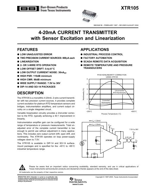
4-20mA CURRENT TRANSMITTER<br />
with Sensor Excitation and Linearization<br />
● LOW UNADJUSTED ERROR<br />
● TWO PRECISION CURRENT SOURCES: 800µA each<br />
● LINEARIZATION<br />
● 2- OR 3-WIRE RTD OPERATION<br />
● LOW OFFSET DRIFT: 0.4µV/°C<br />
● LOW OUTPUT CURRENT NOISE: 30nAPP ● HIGH PSR: 110dB minimum<br />
● HIGH CMR: 86dB minimum<br />
● WIDE SUPPLY RANGE: 7.5V to 36V<br />
● DIP-14 AND SO-14 PACKAGES<br />
DESCRIPTION<br />
The XTR105 is a monolithic 4-20mA, 2-wire current transmitter<br />
with two precision current sources. It provides complete<br />
current excitation for platinum RTD temperature sensors and<br />
bridges, instrumentation amplifiers, and current output circuitry<br />
on a single integrated circuit.<br />
Versatile linearization circuitry provides a 2nd-order correction<br />
to the RTD, typically achieving a 40:1 improvement in<br />
linearity.<br />
Instrumentation amplifier gain can be configured for a wide<br />
range of temperature or pressure measurements. Total unadjusted<br />
error of the complete current transmitter is low<br />
enough to permit use without adjustment in many applications.<br />
This includes zero output current drift, span drift, and<br />
nonlinearity. The XTR105 operates on loop power-supply<br />
voltages down to 7.5V.<br />
The XTR105 is available in DIP-14 and SO-14 surfacemount<br />
packages and is specified for the –40°C to +85°C<br />
industrial temperature range.<br />
APPLICATIONS<br />
● INDUSTRIAL PROCESS CONTROL<br />
● FACTORY AUTOMATION<br />
● SCADA REMOTE DATA ACQUISITION<br />
● REMOTE TEMPERATURE AND PRESSURE<br />
TRANSDUCERS<br />
Nonlinearity (%)<br />
RTD<br />
XTR105<br />
XTR105<br />
5<br />
4<br />
3<br />
2<br />
1<br />
0<br />
–1<br />
–200°C<br />
I R = 0.8mA<br />
I R = 0.8mA<br />
Pt100 NONLINEARITY CORRECTION<br />
USING XTR105<br />
R G<br />
Corrected<br />
Nonlinearity<br />
Process Temperature (°C)<br />
+<br />
–<br />
V LIN<br />
XTR105<br />
V REG<br />
Uncorrected<br />
RTD Nonlinearity<br />
XTR105<br />
SBOS061B – FEBRUARY 1997 – REVISED AUGUST 2004<br />
4-20 mA<br />
+850°C<br />
7.5V to 36V<br />
Please be aware that an important notice concerning availability, standard warranty, and use in critical applications of<br />
Texas Instruments semiconductor products and disclaimers thereto appears at the end of this data sheet.<br />
All trademarks are the property of their respective owners.<br />
PRODUCTION DATA information is current as of publication date.<br />
Products conform to specifications per the terms of Texas Instruments<br />
standard warranty. Production processing does not necessarily include<br />
testing of all parameters.<br />
www.ti.com<br />
V PS<br />
Copyright © 1997-2004, Texas Instruments Incorporated<br />
V O<br />
R L
ABSOLUTE MAXIMUM RATINGS (1)<br />
FUNCTIONAL BLOCK DIAGRAM<br />
2<br />
Power Supply, V+ (referenced to the I O pin) ...................................... 40V<br />
Input Voltage, V IN+, V IN– (referenced to the I O pin) .................... 0V to V+<br />
Storage Temperature Range ......................................... –55°C to +125°C<br />
Lead Temperature (soldering, 10s) ............................................... +300°C<br />
Output Current Limit ................................................................ Continuous<br />
Junction Temperature .................................................................... +165°C<br />
NOTE: (1) Stresses above those listed under “Absolute Maximum Ratings”<br />
may cause permanent damage to the device. Exposure to absolute maximum<br />
conditions for extended periods may affect device reliability.<br />
PACKAGE/ORDERING INFORMATION (1)<br />
PACKAGE<br />
SPECIFIED<br />
TEMPERATURE PACKAGE ORDERING TRANSPORT<br />
PRODUCT PACKAGE-LEAD DESIGNATOR RANGE MARKING NUMBER MEDIA, QUANTITY<br />
XTR105 DIP-14 N –40°C to +85°C XTR105PA XTR105PA Rails, 25<br />
" " " " XTR105P XTR105P Rails, 25<br />
XTR105 SO-14 Surface-Mount D –40°C to +85°C XTR105UA XTR105UA Rails, 58<br />
" " " " XTR105UA XTR105UA/2K5 Tape and Reel, 2500<br />
XTR105 SO-14 Surface-Mount D –40°C to +85°C XTR105U XTR105U Rails, 58<br />
" " " " XTR105U XTR105U/2K5 Tape and Reel, 2500<br />
NOTE: (1) For the most current package and ordering information, see the Package Option Addendum located at the end of this data sheet.<br />
+<br />
VIN –<br />
VIN R G<br />
13<br />
4<br />
3<br />
2<br />
R LIN<br />
1kΩ<br />
VLIN IR1 6<br />
I RET<br />
12 IR2 1<br />
800µA 800µA<br />
100µA<br />
14<br />
VIN I = 100µA +<br />
RG 975Ω<br />
V REG<br />
11<br />
7<br />
5.1V<br />
25Ω<br />
V+<br />
10<br />
B<br />
9<br />
E<br />
8<br />
IO = 4mA + VIN • 40 ( ) RG Q 1<br />
www.ti.com<br />
ELECTROSTATIC<br />
DISCHARGE SENSITIVITY<br />
This integrated circuit can be damaged by ESD. Texas Instruments<br />
recommends that all integrated circuits be handled with<br />
appropriate precautions. Failure to observe proper handling<br />
and installation procedures can cause damage.<br />
ESD damage can range from subtle performance degradation<br />
to complete device failure. Precision integrated circuits<br />
may be more susceptible to damage because very small<br />
parametric changes could cause the device not to meet its<br />
published specifications.<br />
PIN CONFIGURATION<br />
Top View DIP and SO<br />
IR1 1<br />
14 IR2 –<br />
VIN 2<br />
13<br />
+<br />
VIN RG 3<br />
12 VLIN RG 4<br />
11 VREG NC 5<br />
10 V+<br />
I RET<br />
I O<br />
6<br />
7<br />
NC = No Internal Connection<br />
9<br />
8<br />
B (Base)<br />
E (Emitter)<br />
XTR105<br />
SBOS061B
ELECTRICAL <strong>CHARACTERISTICS</strong><br />
At TA = +25°C, V+ = 24V, and TIP29C external transistor, unless otherwise noted.<br />
XTR105P, U XTR105PA, UA<br />
PARAMETER<br />
OUTPUT<br />
CONDITIONS MIN TYP MAX MIN TYP MAX UNITS<br />
Output Current Equation<br />
Output Current, Specified Range 4 20 ✻ ✻<br />
A<br />
mA<br />
Over-Scale Limit 24 27 30 ✻ ✻ ✻ mA<br />
Under-Scale Limit IREG = 0V 1.8 2.2 2.6 ✻ ✻ ✻ mA<br />
ZERO OUTPUT (1) VIN = 0V, RG = ∞ 4 ✻ mA<br />
Initial Error ±5 ±25 ✻ ±50 µA<br />
vs Temperature ±0.07 ±0.5 ✻ ±0.9 µA/°C<br />
vs Supply Voltage, V+ V+ = 7.5V to 36V 0.04 0.2 ✻ ✻ µA/V<br />
vs Common-Mode Voltage VCM = 1.25V to 3.5V (2) IO = VIN • (40/RG) + 4mA, VIN in Volts, RG in Ω<br />
0.02 ✻ µA/V<br />
vs VREG Output Current 0.3 ✻ µA/mA<br />
Noise, 0.1Hz to 10Hz 0.03 ✻ µAPP SPAN<br />
Span Equation (transconductance) S = 40/RG ✻ A/V<br />
Initial Error (3) Full-Scale (VIN) = 50mV ±0.05 ±0.2 ✻ ±0.4 %<br />
vs Temperature (3) ±3 ±25 ✻ ✻ ppm/°C<br />
Nonlinearity, Ideal Input (4) INPUT<br />
Full-Scale (VIN) = 50mV 0.003 0.01 ✻ ✻ %<br />
(5)<br />
Offset Voltage<br />
vs Temperature<br />
VCM = 2V ±50<br />
±0.4<br />
±100<br />
±1.5<br />
✻<br />
✻<br />
±250<br />
±3<br />
µV<br />
µV/°C<br />
vs Supply Voltage, V+ V+ = 7.5V to 36V ±0.3 ±3 ✻ ✻ µV/V<br />
vs Common-Mode Voltage, VCM = 1.25V to 3.5V (2) RTI (CMRR)<br />
±10 ±50 ✻ ±100 µV/V<br />
Common-Mode Input Range (2) 1.25 3.5 ✻ ✻ V<br />
Input Bias Current 5 25 ✻ 50 nA<br />
vs Temperature 20 ✻ pA/°C<br />
Input Offset Current ±0.2 ±3 ✻ ±10 nA<br />
vs Temperature 5 ✻ pA/°C<br />
Impedance, Differential 0.1 || 1 ✻ GΩ || pF<br />
Common-Mode 5 || 10 ✻ GΩ || pF<br />
Noise, 0.1Hz to 10Hz 0.6 ✻ µVPP CURRENT SOURCES V O = 2V (6)<br />
Current 800 ✻ µA<br />
Accuracy ±0.05 ±0.2 ✻ ±0.4 %<br />
vs Temperature ±15 ±35 ✻ ±75 ppm/°C<br />
vs Power Supply, V+ V+ = 7.5V to 36V ±10 ±25 ✻ ✻ ppm/V<br />
Matching ±0.02 ±0.1 ✻ ±0.2 %<br />
vs Temperature ±3 ±15 ✻ ±30 ppm/°C<br />
vs Power Supply, V+ V+ = 7.5V to 36V 1 10 ✻ ✻ ppm/V<br />
Compliance Voltage, Positive (V+) – 3 (V+) – 2.5 ✻ ✻ V<br />
Negative (2) 0 –0.2 ✻ ✻ V<br />
Output Impedance 150 ✻ MΩ<br />
Noise, 0.1Hz to 10Hz 0.003 ✻ µA PP<br />
V (2)<br />
REG 5.1 ✻ V<br />
Accuracy ±0.02 ±0.1 ✻ ✻ V<br />
vs Temperature ±0.2 ✻ mV/°C<br />
vs Supply Voltage, V+ 1 ✻ mV/V<br />
Output Current ±1 ✻ mA<br />
Output Impedance<br />
LINEARIZATION<br />
75 ✻ Ω<br />
RLIN (internal) 1 ✻ kΩ<br />
Accuracy ±0.2 ±0.5 ✻ ±1 %<br />
vs Temperature<br />
POWER SUPPLY<br />
±25 ±100 ✻ ✻ ppm/°C<br />
Specified +24 ✻ V<br />
Voltage Range<br />
TEMPERATURE RANGE<br />
+7.5 +36 ✻ ✻ V<br />
Specification, TMIN to TMAX –40 +85 ✻ ✻ °C<br />
Operating –55 +125 ✻ ✻ °C<br />
Storage<br />
Thermal Resistance, θJA –55 +125 ✻ ✻ °C<br />
DIP-14 80 ✻ °C/W<br />
SO-14 Surface-Mount 100 ✻ °C/W<br />
✻ Specification same as XTR105P and XTR105U.<br />
NOTES: (1) Describes accuracy of the 4mA low-scale offset current. Does not include input amplifier effects. Can be trimmed to zero.<br />
(2) Voltage measured with respect to IRET pin.<br />
(3) Does not include initial error or TCR of gain-setting resistor, RG. (4) Increasing the full-scale input range improves nonlinearity.<br />
(5) Does not include Zero Output initial error.<br />
(6) Current source output voltage with respect to IRET pin.<br />
XTR105 3<br />
SBOS061B www.ti.com
<strong>TYPICAL</strong> <strong>CHARACTERISTICS</strong><br />
At T A = +25°C and V+ = 24V, unless otherwise noted.<br />
4<br />
Transconductance (20 Log mA/V)<br />
Common-Mode Rejection (dB)<br />
Over-Scale Current (mA)<br />
50<br />
40<br />
30<br />
20<br />
10<br />
R G = 500Ω<br />
R G = 2kΩ<br />
TRANSCONDUCTANCE vs FREQUENCY<br />
R G = 125Ω<br />
0<br />
100 1k 10k<br />
Frequency (Hz)<br />
100k<br />
110<br />
100<br />
90<br />
80<br />
70<br />
60<br />
50<br />
40<br />
30<br />
20<br />
10 100 1k 10k 100k<br />
Frequency (Hz)<br />
29<br />
28<br />
27<br />
26<br />
25<br />
24<br />
COMMON-MODE REJECTION vs FREQUENCY<br />
R G = 2kΩ<br />
Full-Scale Input = 50mV<br />
R G = 125Ω<br />
OVER-SCALE CURRENT vs TEMPERATURE<br />
V+ = 36V<br />
With External Transistor<br />
V+ = 24V<br />
V+ = 7.5V<br />
23<br />
–75 –50 –25 0 25 50 75 100<br />
Temperature (°C)<br />
1M<br />
1M<br />
125<br />
4mA/div<br />
www.ti.com<br />
Power Supply Rejection (dB)<br />
Under-Scale Current (mA)<br />
20mA<br />
4mA<br />
140<br />
120<br />
100<br />
80<br />
60<br />
40<br />
20<br />
R G = 2kΩ<br />
R G = 125Ω<br />
STEP RESPONSE<br />
25µs/div<br />
POWER-SUPPLY REJECTION vs FREQUENCY<br />
R G = 2kΩ<br />
R G = 125Ω<br />
0<br />
10 100 1k 10k 100k<br />
Frequency (Hz)<br />
2.40<br />
2.35<br />
2.30<br />
2.25<br />
UNDER-SCALE CURRENT vs TEMPERATURE<br />
2.20<br />
V+ = 7.5V to 36V<br />
2.15<br />
–75 –50 –25 0 25 50 75 100<br />
Temperature (°C)<br />
1M<br />
125<br />
XTR105<br />
SBOS061B
<strong>TYPICAL</strong> <strong>CHARACTERISTICS</strong> (Cont.)<br />
At T A = +25°C and V+ = 24V, unless otherwise noted.<br />
Input Voltage Noise (nV/√Hz)<br />
Input Bias and Offset Current (nA)<br />
Percent of Units (%)<br />
10k<br />
1k<br />
100<br />
INPUT VOLTAGE AND CURRENT<br />
NOISE DENSITY vs FREQUENCY<br />
Current Noise<br />
Voltage Noise<br />
10<br />
1 10 100 1k 10k<br />
Frequency (Hz)<br />
25<br />
20<br />
15<br />
10<br />
5<br />
INPUT BIAS AND OFFSET CURRENT<br />
vs TEMPERATURE<br />
0<br />
–75 –50 –25 0 25 50 75 100<br />
Temperature (°C)<br />
50<br />
45<br />
40<br />
35<br />
30<br />
25<br />
20<br />
15<br />
10<br />
5<br />
0<br />
0.2<br />
0.4<br />
0.6<br />
INPUT OFFSET VOLTAGE DRIFT<br />
PRODUCTION DISTRIBUTION<br />
0.8<br />
1.0<br />
1.2<br />
1.4<br />
I OS<br />
+I B<br />
10k<br />
1k<br />
100<br />
10<br />
100k<br />
–I B<br />
Typical Production Distribution<br />
of Packaged Units.<br />
0.1%<br />
1.6<br />
1.8<br />
2.0<br />
0.02%<br />
2.2<br />
2.4<br />
Input Offset Voltage Drift (µV/°C)<br />
2.6<br />
2.8<br />
3.0<br />
125<br />
Input Current Noise (fA/√Hz)<br />
ZERO OUTPUT AND REFERENCE<br />
CURRENT NOISE vs FREQUENCY<br />
XTR105 5<br />
SBOS061B www.ti.com<br />
Noise (pA/√Hz)<br />
Zero Output Current Error (µA)<br />
Percent of Units (%)<br />
10k<br />
1k<br />
100<br />
Zero Output Current<br />
Reference Current<br />
10<br />
1 10 100 1k 10k<br />
Frequency (Hz)<br />
4<br />
2<br />
0<br />
–2<br />
–4<br />
–6<br />
–8<br />
–10<br />
ZERO OUTPUT CURRENT ERROR<br />
vs TEMPERATURE<br />
–12<br />
–75 –50 –25 0 25 50 75 100<br />
Temperature (°C)<br />
40<br />
35<br />
30<br />
25<br />
20<br />
15<br />
10<br />
5<br />
0<br />
ZERO OUTPUT DRIFT<br />
PRODUCTION DISTRIBUTION<br />
Typical Production Distribution<br />
of Packaged Units.<br />
0.025<br />
0.050<br />
0.075<br />
0.100<br />
0.125<br />
0.150<br />
0.175<br />
0.200<br />
0.225<br />
0.250<br />
0.275<br />
0.300<br />
0.325<br />
0.350<br />
0.375<br />
0.400<br />
0.425<br />
0.450<br />
0.475<br />
0.500<br />
Zero Output Drift (µA/°C)<br />
100k<br />
125
<strong>TYPICAL</strong> <strong>CHARACTERISTICS</strong> (Cont.)<br />
At T A = +25°C and V+ = 24V, unless otherwise noted.<br />
V REG Output Voltage (V)<br />
6<br />
Percent of Units (%)<br />
40<br />
35<br />
30<br />
25<br />
20<br />
15<br />
10<br />
5<br />
0<br />
5.35<br />
5.30<br />
5.25<br />
5.20<br />
5.15<br />
5.10<br />
5.05<br />
5<br />
10<br />
15<br />
CURRENT SOURCE DRIFT<br />
PRODUCTION DISTRIBUTION<br />
20<br />
25<br />
30<br />
35<br />
Typical Production Distribution<br />
of Packaged Units.<br />
I R1 AND I R2 Included.<br />
40<br />
45<br />
50<br />
55<br />
Current Source Drift (ppm/°C)<br />
0.04% 0.01%<br />
60<br />
65<br />
70<br />
V REG OUTPUT VOLTAGE vs V REG OUTPUT CURRENT<br />
–55°C<br />
125°C<br />
25°C<br />
75<br />
NOTE: Above 1mA,<br />
Zero Output Degrades<br />
5.00<br />
–1.0 –0.5 0 0.5 1.0 1.5<br />
VREG Output Current (mA)<br />
2.0<br />
Reference Current Error (%)<br />
www.ti.com<br />
Percent of Units (%)<br />
80<br />
70<br />
60<br />
50<br />
40<br />
30<br />
20<br />
10<br />
0<br />
CURRENT SOURCE MATCHING<br />
DRIFT PRODUCTION DISTRIBUTION<br />
Typical Production Distribution<br />
of Packaged Units.<br />
0.07% 0.02%<br />
2<br />
4<br />
6<br />
8<br />
10<br />
12<br />
14<br />
16<br />
18<br />
20<br />
22<br />
24<br />
26<br />
28<br />
30<br />
+0.05<br />
0<br />
–0.05<br />
–0.10<br />
–0.15<br />
Current Source Matching Drift (ppm/°C)<br />
REFERENCE CURRENT ERROR<br />
vs TEMPERATURE<br />
–0.20<br />
–75 –50 –25 0 25 50 75 100 125<br />
Temperature (°C)<br />
XTR105<br />
SBOS061B
APPLICATION INFORMATION<br />
Figure 1 shows the basic connection diagram for the XTR105.<br />
The loop power supply, VPS, provides power for all circuitry.<br />
Output loop current is measured as a voltage across the<br />
series load resistor, RL. Two matched 0.8mA current sources drive the RTD and<br />
zero-setting resistor, RZ. The instrumentation amplifier input<br />
of the XTR105 measures the voltage difference between the<br />
RTD and RZ. The value of RZ is chosen to be equal to the<br />
resistance of the RTD at the low-scale (minimum) measurement<br />
temperature. RZ can be adjusted to achieve 4mA output<br />
at the minimum measurement temperature to correct for<br />
input offset voltage and reference current mismatch of the<br />
XTR105.<br />
RCM provides an additional voltage drop to bias the inputs of<br />
the XTR105 within their common-mode input range. RCM should be bypassed with a 0.01µF capacitor to minimize<br />
common-mode noise. Resistor RG sets the gain of the instrumentation<br />
amplifier according to the desired temperature<br />
range. RLIN1 provides 2nd-order linearization correction to the<br />
RTD, typically achieving a 40:1 improvement in linearity. An<br />
additional resistor is required for 3-wire RTD connections<br />
(see Figure 3).<br />
RTD<br />
R LIN1 (3)<br />
(1)<br />
RZ R CM = 1kΩ<br />
0.01µF<br />
I R = 0.8mA<br />
I R = 0.8mA<br />
13<br />
(2)<br />
RG 4<br />
3<br />
2<br />
12<br />
1<br />
VLIN IR1 14<br />
+<br />
11<br />
V I<br />
IN<br />
R2 10<br />
VREG<br />
V+<br />
R G<br />
R G<br />
–<br />
VIN I RET<br />
6<br />
XTR105<br />
I O<br />
B<br />
E<br />
7<br />
I = 4mA + VIN • (<br />
40<br />
O<br />
)<br />
RG NOTES: (1) R Z = RTD resistance at minimum measured temperature.<br />
RG = 2R1 (R2 +RZ ) – 4(R2RZ )<br />
(2)<br />
R2 – R1 RLIN (R2 – R1 )<br />
(3) RLIN1 =<br />
2(2R1 – R2 – RZ )<br />
where R1 = RTD Resistance at (TMIN + TMAX )/2<br />
R2 = RTD Resistance at TMAX RLIN = 1kΩ (Internal)<br />
XTR105 7<br />
SBOS061B www.ti.com<br />
9<br />
8<br />
7.5V to 36V<br />
Q 1<br />
Possible choices for Q 1 (see text).<br />
0.01µF<br />
FIGURE 1. Basic 2-Wire RTD Temperature Measurement Circuit with Linearization.<br />
The transfer function through the complete instrumentation<br />
amplifier and voltage-to-current converter is:<br />
IO = 4mA + VIN • (40/RG) (VIN in volts, RG in ohms)<br />
where VIN is the differential input voltage.<br />
As evident from the transfer function, if no RG is used the<br />
gain is zero and the output is simply the XTR105’s zero<br />
current. The value of RG varies slightly for 2-wire RTD and 3wire<br />
RTD connections with linearization. RG can be calculated<br />
from the equations given in Figure 1 (2-wire RTD<br />
connection) and Table I (3-wire RTD connection).<br />
The IRET pin is the return path for all current from the current<br />
sources and VREG. The IRET pin allows any current used in<br />
external circuitry to be sensed by the XTR105 and to be<br />
included in the output current without causing an error.<br />
The VREG pin provides an on-chip voltage source of approximately<br />
5.1V and is suitable for powering external input<br />
circuitry (refer to Figure 6). It is a moderately accurate<br />
voltage reference—it is not the same reference used to set<br />
the 800µA current references. VREG is capable of sourcing<br />
approximately 1mA of current. Exceeding 1mA may affect<br />
the 4mA zero output.<br />
TYPE<br />
2N4922<br />
TIP29C<br />
TIP31C<br />
PACKAGE<br />
TO-225<br />
TO-220<br />
TO-220<br />
R L<br />
I O<br />
4-20 mA<br />
V O<br />
+<br />
VPS –
8<br />
EXAMPLE:<br />
MEASUREMENT TEMPERATURE SPAN ∆T (°C)<br />
TMIN 100°C 200°C 300°C 400°C 500°C 600°C 700°C 800°C 900°C 1000°C<br />
–200°C 18.7/86.6 18.7/169 18.7/255 18.7/340 18.7/422 18.7/511 18.7/590 18.7/665 18.7/750 18.7/845<br />
15000 9760 8060 6650 5620 4750 4020 3480 3090 2740<br />
16500 11500 10000 8870 7870 7150 6420 5900 5360 4990<br />
–100°C 60.4/80.6 60.4/162 60.4/243 60.4/324 60.4/402 60.4/487 60.4/562 60.4/649 60.4/732<br />
27400 15400 10500 7870 6040 4990 4220 3570 3090<br />
29400 17800 13000 10200 8660 7500 6490 5900 5360<br />
0°C 100/78.7 100/158 100/237 100/316 100/392 100/475 100/549 100/634<br />
33200 16200 10500 7680 6040 4870 4020 3480<br />
35700 18700 13000 10000 8250 7150 6340 5620<br />
100°C 137/75 137/150 137/226 137/301 137/383 137/453 137/536<br />
31600 15400 10200 7500 5760 4750 3920<br />
34000 17800 12400 9760 8060 6810 6040<br />
200°C 174/73.2 174/147 174/221 174/294 174/365 174/442<br />
30900 15000 9760 7150 5620 4530<br />
33200 17400 12100 9310 7680 6490<br />
300°C 210/71.5 210/143 210/215 210/287 210/357<br />
30100 14700 9530 6980 5360<br />
32400 16500 11500 8870 7320<br />
400°C 249/68.1 249/137 249/205 249/274<br />
28700 14000 9090 6650<br />
30900 16200 11000 8450<br />
500°C 280/66.5 280/133 280/200<br />
28000 13700 8870<br />
30100 15400 10500<br />
600°C 316/64.9 313/130<br />
26700 13000<br />
28700 14700<br />
700°C 348/61.9<br />
26100<br />
27400<br />
800°C 374/60.4<br />
24900<br />
26700<br />
www.ti.com<br />
R G = 2(R 2 – R Z )(R 1 – R Z )<br />
(R 2 – R 1)<br />
R LIN1 = R LIN(R 2 – R 1)<br />
2(2R 1 – R 2 – R Z)<br />
R LIN2 = (R LIN + R G )(R 2 – R 1)<br />
2(2R 1 – R 2 – R Z)<br />
R Z /R G<br />
R LIN1<br />
R LIN2<br />
where: R 1 = RTD resistance at (T MIN + T MAX )/2<br />
R 2 = RTD resistance at T MAX<br />
R LIN = 1kΩ (Internal)<br />
The measurement range is –100°C to +200°C for a 3-wire Pt100 RTD connection. Determine the values for R S, R G, R LIN1, and R LIN2. Look up the values<br />
from the chart or calculate the values according to the equations provided.<br />
METHOD 1: TABLE LOOK UP<br />
For TMIN = –100°C and ∆T = –300°C, the 1% values are:<br />
RZ = 60.4Ω RLIN1 = 10.5kΩ<br />
RG = 243Ω RLIN2 = 13kΩ<br />
METHOD 2: CALCULATION<br />
Step 1: Determine RZ, R1, and R2. RZ is the RTD resistance at the minimum measured temperature,TMIN = –100°C.<br />
Using Equation 1 at right gives RZ = 60.25Ω (1% value is 60.4Ω).<br />
R2 is the RTD resistance at the maximum measured temperature, TMAX = 200°C.<br />
Using Equation 2 at right gives R2 = 175.84Ω.<br />
R1 is the RTD resistance at the midpoint measured temperature,<br />
TMID = (TMIN + TMAX) /2 = 50°C. R1 is NOT the average of RZ and R2. Using Equation 2 at right gives R1 = 119.40Ω.<br />
Step 2: Calculate RG, RLIN1, and RLIN2 using equations above.<br />
RG = 242.3Ω (1% value is 243Ω)<br />
RLIN1 = 10.413kΩ (1% value is 10.5kΩ)<br />
RLIN2 = 12.936kΩ (1% value is 13kΩ)<br />
Calculation of Pt100 Resistance Values<br />
(according to DIN IEC 751)<br />
(Equation 1) Temperature range from –200°C to 0°C:<br />
R (T) = 100 [1 + 3.90802 • 10 –3 • T – 0.5802 • 10 –6 •<br />
T2 – 4.27350 • 10 –12 (T – 100) T3 ]<br />
(Equation 2) Temperature range from 0°C to +850°C:<br />
R (T) = 100 (1 + 3.90802 • 10 –3 • T – 0.5802 • 10 –6 • T 2)<br />
where: R (T) is the resistance in Ω at temperature T.<br />
T is the temperature in °C.<br />
TABLE I. R Z, R G, R LIN1, and R LIN2 Standard 1% Resistor Values for 3-Wire Pt100 RTD Connection with Linearization.<br />
A negative input voltage, V IN, will cause the output current to<br />
be less than 4mA. Increasingly negative V IN will cause the<br />
output current to limit at approximately 2.2mA. Refer to the<br />
typical characteristic Under-Scale Current vs Temperature.<br />
NOTE: The values listed in this table are 1% resistors (in Ω).<br />
Exact values may be calculated from the following equations:<br />
RZ = RTD resistance at minimum measured temperature.<br />
NOTE: Most RTD manufacturers provide reference tables for<br />
resistance values at various temperatures.<br />
Increasingly positive input voltage (greater than the full-scale<br />
input) will produce increasing output current according to the<br />
transfer function, up to the output current limit of approximately<br />
27mA. Refer to the typical characteristic Over-Scale<br />
Current vs Temperature.<br />
XTR105<br />
SBOS061B
EXTERNAL TRANSISTOR<br />
Transistor Q1 conducts the majority of the signal-dependent<br />
4-20mA loop current. Using an external transistor isolates<br />
the majority of the power dissipation from the precision input<br />
and reference circuitry of the XTR105, maintaining excellent<br />
accuracy.<br />
Since the external transistor is inside a feedback loop, its<br />
characteristics are not critical. Requirements are: VCEO = 45V<br />
min, β = 40 min, and PD = 800mW. Power dissipation<br />
requirements may be lower if the loop power-supply voltage<br />
is less than 36V. Some possible choices for Q1 are listed in<br />
Figure 1.<br />
The XTR105 can be operated without this external transistor,<br />
however, accuracy will be somewhat degraded due to<br />
the internal power dissipation. Operation without Q1 is not<br />
recommended for extended temperature ranges. A resistor<br />
(R = 3.3kΩ) connected between the IRET pin and the E<br />
(emitter) pin may be needed for operation below 0°C without<br />
Q1 to ensure the full 20mA full-scale output, especially<br />
with V+ near 7.5V.<br />
I RET<br />
6<br />
V+<br />
E<br />
8<br />
XTR105 0.01µF<br />
I O<br />
R Q = 3.3kΩ<br />
10<br />
7<br />
For operation without an external<br />
transistor, connect a 3.3kΩ<br />
resistor between pin 6 and pin 8.<br />
See text for discussion<br />
of performance.<br />
FIGURE 2. Operation Without an External Transistor.<br />
LOOP POWER SUPPLY<br />
The voltage applied to the XTR105, V+, is measured with<br />
respect to the IO connection, pin 7. V+ can range from 7.5V<br />
to 36V. The loop-supply voltage, VPS, will differ from the<br />
voltage applied to the XTR105 according to the voltage drop<br />
on the current sensing resistor, RL (plus any other voltage<br />
drop in the line).<br />
If a low loop-supply voltage is used, RL (including the loop<br />
wiring resistance) must be made a relatively low value to<br />
assure that V+ remains 7.5V or greater for the maximum loop<br />
current of 20mA:<br />
⎛ ( V+ )– 75 . V⎞<br />
RL<br />
max = ⎜<br />
⎟ – RWIRING<br />
⎝ 20mA<br />
⎠<br />
It is recommended to design for V+ equal or greater than<br />
7.5V with loop currents up to 30mA to allow for out-of-range<br />
input conditions.<br />
The low operating voltage (7.5V) of the XTR105 allows<br />
operation directly from personal computer power supplies<br />
(12V ±5%). When used with the RCV420 current loop receiver<br />
(see Figure 7), the load resistor voltage drop is limited<br />
to 3V.<br />
ADJUSTING INITIAL ERRORS<br />
Many applications require adjustment of initial errors. Input<br />
offset and reference current mismatch errors can be corrected<br />
by adjustment of the zero resistor, RZ. Adjusting the<br />
gain-setting resistor, RG, corrects any errors associated with<br />
gain.<br />
2- AND 3-WIRE RTD CONNECTIONS<br />
In Figure 1, the RTD can be located remotely simply by<br />
extending the two connections to the RTD. With this remote<br />
2-wire connection to the RTD, line resistance will introduce<br />
error. This error can be partially corrected by adjusting the<br />
values of RZ, RG, and RLIN1. A better method for remotely located RTDs is the 3-wire RTD<br />
connection (see Figure 3). This circuit offers improved accuracy.<br />
RZ’s current is routed through a third wire to the RTD.<br />
Assuming line resistance is equal in RTD lines 1 and 2, this<br />
produces a small common-mode voltage that is rejected by<br />
the XTR105. A second resistor, RLIN2, is required for linearization.<br />
Note that although the 2-wire and 3-wire RTD connection<br />
circuits are very similar, the gain-setting resistor, RG, has<br />
slightly different equations:<br />
2-wire:<br />
3-wire:<br />
XTR105 9<br />
SBOS061B www.ti.com<br />
R<br />
G<br />
R<br />
2R R R R R<br />
= 1( 2 + Z)– 4(<br />
2 Z)<br />
R – R<br />
G<br />
2 1<br />
R R R R<br />
= Z Z<br />
R R<br />
2( 2 – )( 1–<br />
)<br />
–<br />
2 1<br />
where: RZ = RTD resistance at TMIN R1 = RTD resistance at (TMIN + TMAX)/2 R2 = RTD resistance at TMAX To maintain good accuracy, at least 1% (or better) resistors<br />
should be used for RG. Table I provides standard 1% RG resistor values for a 3-wire Pt100 RTD connection with<br />
linearization.<br />
LINEARIZATION<br />
RTD temperature sensors are inherently (but predictably)<br />
nonlinear. With the addition of one or two external resistors,<br />
RLIN1 and RLIN2, it is possible to compensate for most of this<br />
nonlinearity resulting in 40:1 improvement in linearity over<br />
the uncompensated output.<br />
See Figure 1 for a typical 2-wire RTD application with<br />
linearization. Resistor RLIN1 provides positive feedback and<br />
controls linearity correction. RLIN1 is chosen according to the<br />
desired temperature range. An equation is given in Figure 1.
In 3-wire RTD connections, an additional resistor, RLIN2, is<br />
required. As with the 2-wire RTD application, RLIN1 provides<br />
positive feedback for linearization. RLIN2 provides an offset<br />
canceling current to compensate for wiring resistance encountered<br />
in remotely located RTDs. RLIN1 and RLIN2 are<br />
chosen such that their currents are equal. This makes the<br />
voltage drop in the wiring resistance to the RTD a commonmode<br />
signal that is rejected by the XTR105. The nearest<br />
standard 1% resistor values for RLIN1 and RLIN2 should be<br />
adequate for most applications. Table I provides the 1%<br />
resistor values for a 3-wire Pt100 RTD connection.<br />
If no linearity correction is desired, the VLIN pin should be left<br />
open. With no linearization, RG = 2500 • VFS, where<br />
VFS = full-scale input range.<br />
RTDs<br />
The text and figures thus far have assumed a Pt100 RTD. With<br />
higher resistance RTDs, the temperature range and input<br />
voltage variation should be evaluated to ensure proper common-mode<br />
biasing of the inputs. As mentioned earlier, RCM can<br />
be adjusted to provide an additional voltage drop to bias the<br />
inputs of the XTR105 within their common-mode input range.<br />
Resistance in this line causes<br />
a small common-mode voltage<br />
which is rejected by the XTR105.<br />
FIGURE 3. Remotely Located RTDs with 3-Wire Connection.<br />
10<br />
EQUAL line resistances here<br />
creates a small common-mode<br />
voltage which is rejected by<br />
the XTR105.<br />
RTD<br />
R LIN1 (1)<br />
2 1<br />
R Z (1)<br />
(R LINE2 ) (R LINE1 )<br />
3<br />
(R LINE3 )<br />
R LIN2 (1)<br />
Q 2 (2)<br />
2N2222<br />
www.ti.com<br />
ERROR ANALYSIS<br />
See Table II for how to calculate the effect various error<br />
sources have on circuit accuracy. A sample error calculation<br />
for a typical RTD measurement circuit (Pt100 RTD, 200°C<br />
measurement span) is provided. The results reveal the<br />
XTR105’s excellent accuracy, in this case 1.1% unadjusted.<br />
Adjusting resistors RG and RZ for gain and offset errors<br />
improves circuit accuracy to 0.32%. Note that these are<br />
worst-case errors; ensured maximum values were used in<br />
the calculations and all errors were assumed to be positive<br />
(additive). The XTR105 achieves performance that is difficult<br />
to obtain with discrete circuitry and requires less space.<br />
OPEN-CIRCUIT PROTECTION<br />
The optional transistor Q2 in Figure 3 provides predictable<br />
behavior with open-circuit RTD connections. It assures that<br />
if any one of the three RTD connections is broken, the<br />
XTR105’s output current will go to either its high current limit<br />
(≈ 27mA) or low current limit (≈ 2.2mA). This is easily<br />
detected as an out-of-range condition.<br />
13<br />
(1)<br />
RG 4<br />
3<br />
2<br />
12<br />
1<br />
VLIN 14<br />
IR1<br />
+ I 11<br />
R2 V 10<br />
IN<br />
VREG<br />
V+<br />
R G<br />
R G<br />
–<br />
VIN I RET<br />
6<br />
XTR105<br />
I O<br />
B<br />
E<br />
R CM = 1000Ω 0.01µF<br />
7<br />
9<br />
8<br />
Q 1<br />
OPEN RTD<br />
TERMINAL<br />
1<br />
2<br />
3<br />
0.01µF<br />
NOTES: (1) See Table I for resistor equations and<br />
1% values. (2) Q 2 optional. Provides predictable<br />
output current if any one RTD connection is<br />
broken:<br />
I O<br />
I O<br />
I O<br />
≈ 2.2mA<br />
≈27mA<br />
≈2.2mA<br />
XTR105<br />
SBOS061B
RTD value at 4mA Output (R RTD MIN): 100Ω<br />
RTD Measurement Range: 200°C<br />
Ambient Temperature Range (∆T A): 20°C<br />
Supply Voltage Change (∆V+): 5V<br />
Common-Mode Voltage Change (∆CM): 0.1V<br />
TABLE II. Error Calculation.<br />
SAMPLE ERROR CALCULATION<br />
SAMPLE<br />
ERROR SOURCE ERROR EQUATION ERROR CALCULATION (1) ERROR<br />
(ppm of Full Scale)<br />
UNADJ. ADJUST.<br />
INPUT<br />
Input Offset Voltage VOS/(VIN MAX) • 106 100µV/(800µA • 0.38Ω/°C • 200°C) • 106 1645 0<br />
vs Common-Mode CMRR • ∆CM/(VIN MAX) • 106 50µV/V • 0.1V/(800µA • 0.38Ω/°C • 200°C) • 106 82 82<br />
Input Bias Current IB/IREF • 106 0.025µA/800µA • 106 31 0<br />
Input Offset Current IOS • RRTD MIN/(VIN MAX) • 106 3nA • 100Ω/(800µA • 0.38Ω/°C • 200°C) • 106 5 0<br />
EXCITATION<br />
Total Input Error: 1763 82<br />
Current Reference Accuracy IREF Accuracy (%)/100% • 106 0.2%/100% • 106 2000 0<br />
vs Supply (IREF vs V+) • ∆V+ 25ppm/V • 5V 125 125<br />
Current Reference Matching IREF Matching (%)/100% • 800µA • 0.1%/100% • 800µA • 100Ω/(800µA • 0.38Ω/°C • 200°C) • 106 RRTD MIN/(VIN MAX) • 10<br />
1316 0<br />
6<br />
vs Supply (IREF Matching vs V+) • ∆V+ •<br />
RRTD MIN/(VIN MAX)<br />
10ppm/V • 5V • 800µA • 100Ω/(800µA • 0.38Ω/°C • 200°C) 66 66<br />
GAIN<br />
Total Excitation Error: 3507 191<br />
Span Span Error (%)/100% • 106 0.2%/100% • 106 2000 0<br />
Nonlinearity Nonlinearity (%)/100% • 106 0.01%/100% • 106 100 100<br />
OUTPUT<br />
Total Gain Error: 2100 100<br />
Zero Output (IZERO – 4mA) /16000µA • 106 25µA/16000µA • 106 1563 0<br />
vs Supply (IZERO vs V+) • ∆V+/16000µA • 106 0.2µA/V • 5V/16000µA • 106 63 63<br />
DRIFT (∆TA = 20°C)<br />
Total Output Error: 1626 63<br />
Input Offset Voltage Drift • ∆TA/(VIN MAX) • 106 1.5µV/°C • 20°C/(800µA • 0.38Ω/°C • 200°C) • 106 493 493<br />
Input Bias Current (typical) Drift • ∆TA/800µA • 106 20pA/°C • 20°C/800µA • 106 0.5 0.5<br />
Input Offset Current (typical) Drift • ∆TA • RRTD MIN/(VIN MAX) • 106 5pA/°C • 20°C • 100W/(800µA • 0.38Ω/°C • 200°C) • 106 0.2 0.2<br />
Current Reference Accuracy Drift • ∆TA 35ppm/°C • 20°C 700 700<br />
Current Reference Matching Drift • ∆TA • 800µA • RRTD MIN/(VIN MAX) 15ppm/°C • 20°C • 800µA • 100Ω/(800µA • 0.38Ω/°C • 200°C) 395 395<br />
Span Drift • ∆TA 25ppm/°C • 20°C 500 500<br />
Zero Output Drift • ∆TA/16000µA • 106 0.5µA/°C • 20°C/16000µA • 106 626 626<br />
NOISE (0.1Hz to 10Hz, typ)<br />
Total Drift Error: 2715 2715<br />
Input Offset Voltage vn/(VIN MAX) • 106 0.6µV/(800µA • 0.38Ω/°C • 200°C) • 106 10 10<br />
Current Reference IREF Noise • RRTD MIN/(VIN MAX) • 106 3nA • 100Ω/(800µA • 0.38Ω/°C • 200°C) • 106 5 5<br />
Zero Output IZERO Noise/16000µA • 106 0.03µA/16000µA • 106 2 2<br />
Total Noise Error: 17 17<br />
NOTE (1): All errors are min/max and referred to input unless otherwise stated.<br />
TOTAL ERROR: 11728 3168<br />
(1.17%) (0.32%)<br />
XTR105 11<br />
SBOS061B www.ti.com
REVERSE-VOLTAGE PROTECTION<br />
The XTR105’s low compliance rating (7.5V) permits the use<br />
of various voltage protection methods without compromising<br />
operating range. Figure 4 shows a diode bridge circuit that<br />
allows normal operation even when the voltage connection<br />
lines are reversed. The bridge causes a two diode drop<br />
(approximately 1.4V) loss in loop-supply voltage. This results<br />
in a compliance voltage of approximately 9V—satisfactory<br />
for most applications. If a 1.4V drop in loop supply is too<br />
much, a diode can be inserted in series with the loop-supply<br />
voltage and the V+ pin. This protects against reverse output<br />
connection lines with only a 0.7V loss in loop-supply voltage.<br />
SURGE PROTECTION<br />
Remote connections to current transmitters can sometimes be<br />
subjected to voltage surges. It is prudent to limit the maximum<br />
surge voltage applied to the XTR105 to as low as practical.<br />
Various zener diodes and surge clamping diodes are specially<br />
designed for this purpose. Select a clamp diode with as low a<br />
voltage rating as possible for best protection. For example, a<br />
36V protection diode will assure proper transmitter operation<br />
at normal loop voltages, yet will provide an appropriate level<br />
of protection against voltage surges. Characterization tests on<br />
three production lots showed no damage to the XTR105 within<br />
loop-supply voltages up to 65V.<br />
12<br />
I RET<br />
XTR105<br />
6<br />
V+<br />
I O<br />
10<br />
B<br />
E<br />
7<br />
9<br />
8<br />
0.01µF<br />
D 1 (1)<br />
1N4148<br />
Diodes<br />
The diode bridge causes<br />
a 1.4V loss in loop-supply<br />
voltage.<br />
FIGURE 4. Reverse Voltage Operation and Over-Voltage Surge Protection.<br />
www.ti.com<br />
Most surge protection zener diodes have a diode characteristic<br />
in the forward direction that will conduct excessive<br />
current, possibly damaging receiving-side circuitry if the loop<br />
connections are reversed. If a surge protection diode is used,<br />
a series diode or diode bridge should be used for protection<br />
against reversed connections.<br />
RADIO FREQUENCY INTERFERENCE<br />
The long wire lengths of current loops invite radio frequency<br />
(RF) interference. RF can be rectified by the sensitive input<br />
circuitry of the XTR105 causing errors. This generally appears<br />
as an unstable output current that varies with the<br />
position of loop supply or input wiring.<br />
If the RTD sensor is remotely located, the interference may<br />
enter at the input terminals. For integrated transmitter assemblies<br />
with short connections to the sensor, the interference<br />
more likely comes from the current loop connections.<br />
Bypass capacitors on the input reduce or eliminate this input<br />
interference. Connect these bypass capacitors to the IRET terminal (see Figure 5). Although the dc voltage at the IRET terminal is not equal to 0V (at the loop supply, VPS), this<br />
circuit point can be considered the transmitter’s “ground.”<br />
The 0.01µF capacitor connected between V+ and IO may<br />
help minimize output interference.<br />
NOTE: (1) Zener Diode 36V: 1N4753A or General<br />
Semiconductor Transorb TM 1N6286A. Use lower<br />
voltage zener diodes with loop-power supply<br />
voltages less than 30V for increased protection.<br />
See the Surge Protection section.<br />
R L<br />
V PS<br />
Maximum V PS must be<br />
less than minimum<br />
voltage rating of zener<br />
diode.<br />
XTR105<br />
SBOS061B
Type J<br />
R LIN1<br />
RTD<br />
R LIN2<br />
FIGURE 5. Input Bypassing Technique with Linearization.<br />
50Ω<br />
R Z<br />
R CM<br />
1kΩ<br />
25Ω<br />
1kΩ<br />
1kΩ<br />
0.01µF 0.01µF<br />
0.01µF<br />
(1)<br />
R<br />
412Ω<br />
R CM = 1250Ω<br />
V+<br />
1/2<br />
OPA2335<br />
R F<br />
10kΩ<br />
R F<br />
10kΩ<br />
1/2<br />
OPA2335<br />
I REG < 1mA<br />
FIGURE 6. Thermocouple Low Offset, Low Drift Loop Measurement with Diode Cold Junction Compensation.<br />
V–<br />
R G<br />
13<br />
4<br />
3<br />
2<br />
2RF (G = 1 + = 50)<br />
R<br />
12<br />
1<br />
VLIN IR1 14<br />
+<br />
11<br />
V I<br />
IN<br />
R2 10<br />
VREG<br />
V+<br />
XTR105 13<br />
SBOS061B www.ti.com<br />
R G<br />
R G<br />
–<br />
VIN I RET<br />
13<br />
R G<br />
1250Ω<br />
XTR105<br />
NOTE: (1) Bypass capacitors can be connected<br />
to either the I RET pin or the I O pin.<br />
6<br />
4<br />
3<br />
2<br />
12<br />
V 1<br />
LIN<br />
I<br />
+<br />
R1<br />
VIN R G<br />
R G<br />
–<br />
VIN I RET<br />
6<br />
I O<br />
B<br />
E<br />
7<br />
5V<br />
14<br />
I<br />
11<br />
R2 10<br />
VREG V+<br />
XTR105<br />
9<br />
8<br />
B<br />
9<br />
E<br />
8<br />
IO 7<br />
0.01µF<br />
+ –<br />
IO = 4mA + (VIN – VIN )<br />
40<br />
RG
Pt100<br />
100°C to<br />
600°C<br />
FIGURE 7. ±12V Powered Transmitter/Receiver Loop.<br />
14<br />
RTD<br />
RTD<br />
R LIN1<br />
R LIN1<br />
5760Ω<br />
R Z<br />
R Z<br />
137Ω<br />
R CM = 1kΩ<br />
R LIN2<br />
0.01µF<br />
R CM = 1kΩ<br />
0.01µF<br />
13<br />
4<br />
R G<br />
402Ω<br />
3<br />
2<br />
12<br />
1<br />
VLIN IR1 14<br />
+<br />
11<br />
V I<br />
IN<br />
R2 10<br />
VREG<br />
V+<br />
R G<br />
R G<br />
–<br />
VIN I RET<br />
FIGURE 8. Isolated Transmitter/Receiver Loop.<br />
6<br />
XTR105<br />
12<br />
1<br />
VLIN 13 IR1 14<br />
+ I<br />
11<br />
VIN R2 10<br />
VREG<br />
V+<br />
R G<br />
4<br />
3<br />
2<br />
R G<br />
R G<br />
–<br />
VIN IRET 6<br />
XTR105<br />
9<br />
B<br />
E<br />
8<br />
I O<br />
7<br />
I O<br />
B 9<br />
E 8<br />
7<br />
Q 1<br />
I O = 4mA – 20mA<br />
www.ti.com<br />
1N4148<br />
0.01µF<br />
NOTE: A 2-wire RTD connection is shown. For remotely<br />
located RTDs, a 3-wire RTD conection is recommended.<br />
R G becomes 383Ω, R LIN2 is 8060Ω. See Figure 3 and<br />
Table I.<br />
Q 1<br />
I O = 4mA – 20mA<br />
1N4148<br />
0.01µF<br />
NOTE: A 3-wire RTD connection is shown.<br />
For a 2-wire RTD connection eliminate R LIN2 .<br />
16<br />
10<br />
3<br />
11<br />
12<br />
2<br />
RCV420<br />
13<br />
15<br />
14<br />
4<br />
5<br />
+12V<br />
16<br />
3<br />
10<br />
11<br />
12<br />
2<br />
RCV420<br />
13<br />
15<br />
14<br />
4<br />
–12V<br />
1µF<br />
5<br />
1µF<br />
15<br />
1µF<br />
1µF<br />
1<br />
ISO122<br />
16 2<br />
10 8<br />
9<br />
7<br />
V O = 0 to 5V<br />
+15V<br />
Isolated Power<br />
0<br />
from PWS740<br />
–15V<br />
V+<br />
VO 0 – 5V<br />
V–<br />
XTR105<br />
SBOS061B
1.6mA<br />
FIGURE 9. Bridge Input, Current Excitation.<br />
R G<br />
R CM = 1kΩ (1)<br />
12<br />
1<br />
VLIN I<br />
+ R1<br />
13 VIN 4<br />
3<br />
2<br />
R G<br />
R G<br />
–<br />
VIN I RET<br />
6<br />
14<br />
I<br />
11<br />
R2<br />
V<br />
10<br />
REG<br />
V+<br />
XTR105<br />
XTR105 15<br />
SBOS061B www.ti.com<br />
B<br />
E<br />
7<br />
9<br />
8<br />
NOTE: (1) Use R CM to adjust the<br />
common-mode voltage to within<br />
1.25V to 3.5V.
PACKAGING INFORMATION<br />
Orderable Device Status (1)<br />
Package<br />
Type<br />
Package<br />
Drawing<br />
Pins Package<br />
Qty<br />
Eco Plan (2) Lead/Ball Finish MSL Peak Temp (3)<br />
XTR105P ACTIVE PDIP N 14 25 TBD CU SNPB Level-NA-NA-NA<br />
XTR105PA ACTIVE PDIP N 14 25 TBD CU SNPB Level-NA-NA-NA<br />
XTR105U ACTIVE SOIC D 14 58 Pb-Free<br />
(RoHS)<br />
XTR105UA ACTIVE SOIC D 14 58 Pb-Free<br />
(RoHS)<br />
XTR105UA/2K5 ACTIVE SOIC D 14 2500 Pb-Free<br />
(RoHS)<br />
CU NIPDAU Level-3-260C-168 HR<br />
CU NIPDAU Level-3-260C-168 HR<br />
CU NIPDAU Level-3-260C-168 HR<br />
(1) The marketing status values are defined as follows:<br />
ACTIVE: Product device recommended for new designs.<br />
LIFEBUY: TI has announced that the device will be discontinued, and a lifetime-buy period is in effect.<br />
NRND: Not recommended for new designs. Device is in production to support existing customers, but TI does not recommend using this part in<br />
a new design.<br />
PREVIEW: Device has been announced but is not in production. Samples may or may not be available.<br />
OBSOLETE: TI has discontinued the production of the device.<br />
(2) Eco Plan - The planned eco-friendly classification: Pb-Free (RoHS) or Green (RoHS & no Sb/Br) - please check<br />
http://www.ti.com/productcontent for the latest availability information and additional product content details.<br />
TBD: The Pb-Free/Green conversion plan has not been defined.<br />
Pb-Free (RoHS): TI's terms "Lead-Free" or "Pb-Free" mean semiconductor products that are compatible with the current RoHS requirements<br />
for all 6 substances, including the requirement that lead not exceed 0.1% by weight in homogeneous materials. Where designed to be soldered<br />
at high temperatures, TI Pb-Free products are suitable for use in specified lead-free processes.<br />
Green (RoHS & no Sb/Br): TI defines "Green" to mean Pb-Free (RoHS compatible), and free of Bromine (Br) and Antimony (Sb) based flame<br />
retardants (Br or Sb do not exceed 0.1% by weight in homogeneous material)<br />
(3) MSL, Peak Temp. -- The Moisture Sensitivity Level rating according to the JEDEC industry standard classifications, and peak solder<br />
temperature.<br />
PACKAGE OPTION ADDENDUM<br />
www.ti.com 8-Nov-2005<br />
Important Information and Disclaimer:The information provided on this page represents TI's knowledge and belief as of the date that it is<br />
provided. TI bases its knowledge and belief on information provided by third parties, and makes no representation or warranty as to the<br />
accuracy of such information. Efforts are underway to better integrate information from third parties. TI has taken and continues to take<br />
reasonable steps to provide representative and accurate information but may not have conducted destructive testing or chemical analysis on<br />
incoming materials and chemicals. TI and TI suppliers consider certain information to be proprietary, and thus CAS numbers and other limited<br />
information may not be available for release.<br />
In no event shall TI's liability arising out of such information exceed the total purchase price of the TI part(s) at issue in this document sold by TI<br />
to Customer on an annual basis.<br />
Addendum-Page 1
IMPORTANT NOTICE<br />
Texas Instruments Incorporated and its subsidiaries (TI) reserve the right to make corrections, modifications,<br />
enhancements, improvements, and other changes to its products and services at any time and to discontinue<br />
any product or service without notice. Customers should obtain the latest relevant information before placing<br />
orders and should verify that such information is current and complete. All products are sold subject to TI’s terms<br />
and conditions of sale supplied at the time of order acknowledgment.<br />
TI warrants performance of its hardware products to the specifications applicable at the time of sale in<br />
accordance with TI’s standard warranty. Testing and other quality control techniques are used to the extent TI<br />
deems necessary to support this warranty. Except where mandated by government requirements, testing of all<br />
parameters of each product is not necessarily performed.<br />
TI assumes no liability for applications assistance or customer product design. Customers are responsible for<br />
their products and applications using TI components. To minimize the risks associated with customer products<br />
and applications, customers should provide adequate design and operating safeguards.<br />
TI does not warrant or represent that any license, either express or implied, is granted under any TI patent right,<br />
copyright, mask work right, or other TI intellectual property right relating to any combination, machine, or process<br />
in which TI products or services are used. Information published by TI regarding third-party products or services<br />
does not constitute a license from TI to use such products or services or a warranty or endorsement thereof.<br />
Use of such information may require a license from a third party under the patents or other intellectual property<br />
of the third party, or a license from TI under the patents or other intellectual property of TI.<br />
Reproduction of information in TI data books or data sheets is permissible only if reproduction is without<br />
alteration and is accompanied by all associated warranties, conditions, limitations, and notices. Reproduction<br />
of this information with alteration is an unfair and deceptive business practice. TI is not responsible or liable for<br />
such altered documentation.<br />
Resale of TI products or services with statements different from or beyond the parameters stated by TI for that<br />
product or service voids all express and any implied warranties for the associated TI product or service and<br />
is an unfair and deceptive business practice. TI is not responsible or liable for any such statements.<br />
Following are URLs where you can obtain information on other Texas Instruments products and application<br />
solutions:<br />
Products Applications<br />
Amplifiers amplifier.ti.com Audio www.ti.com/audio<br />
Data Converters dataconverter.ti.com Automotive www.ti.com/automotive<br />
DSP dsp.ti.com Broadband www.ti.com/broadband<br />
Interface interface.ti.com Digital Control www.ti.com/digitalcontrol<br />
Logic logic.ti.com Military www.ti.com/military<br />
Power Mgmt power.ti.com Optical Networking www.ti.com/opticalnetwork<br />
Microcontrollers microcontroller.ti.com Security www.ti.com/security<br />
Telephony www.ti.com/telephony<br />
Video & Imaging www.ti.com/video<br />
Wireless www.ti.com/wireless<br />
Mailing Address: Texas Instruments<br />
Post Office Box 655303 Dallas, Texas 75265<br />
Copyright © 2005, Texas Instruments Incorporated