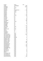
TYPICAL CHARACTERISTICS - Adronic Components GmbH
TYPICAL CHARACTERISTICS - Adronic Components GmbH
TYPICAL CHARACTERISTICS - Adronic Components GmbH

Create successful ePaper yourself
Turn your PDF publications into a flip-book with our unique Google optimized e-Paper software.
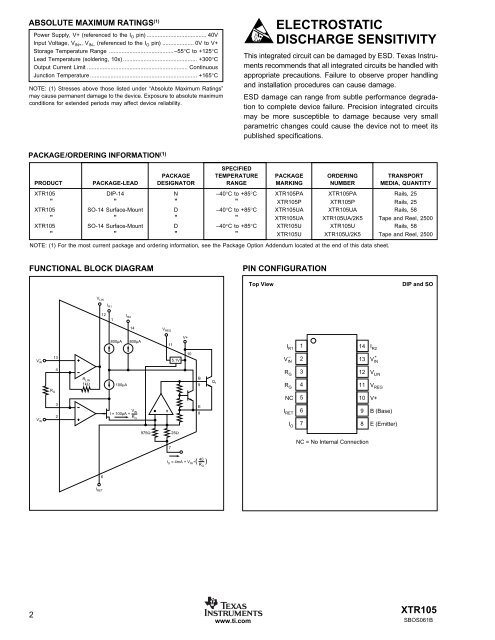
ABSOLUTE MAXIMUM RATINGS (1)<br />
FUNCTIONAL BLOCK DIAGRAM<br />
2<br />
Power Supply, V+ (referenced to the I O pin) ...................................... 40V<br />
Input Voltage, V IN+, V IN– (referenced to the I O pin) .................... 0V to V+<br />
Storage Temperature Range ......................................... –55°C to +125°C<br />
Lead Temperature (soldering, 10s) ............................................... +300°C<br />
Output Current Limit ................................................................ Continuous<br />
Junction Temperature .................................................................... +165°C<br />
NOTE: (1) Stresses above those listed under “Absolute Maximum Ratings”<br />
may cause permanent damage to the device. Exposure to absolute maximum<br />
conditions for extended periods may affect device reliability.<br />
PACKAGE/ORDERING INFORMATION (1)<br />
PACKAGE<br />
SPECIFIED<br />
TEMPERATURE PACKAGE ORDERING TRANSPORT<br />
PRODUCT PACKAGE-LEAD DESIGNATOR RANGE MARKING NUMBER MEDIA, QUANTITY<br />
XTR105 DIP-14 N –40°C to +85°C XTR105PA XTR105PA Rails, 25<br />
" " " " XTR105P XTR105P Rails, 25<br />
XTR105 SO-14 Surface-Mount D –40°C to +85°C XTR105UA XTR105UA Rails, 58<br />
" " " " XTR105UA XTR105UA/2K5 Tape and Reel, 2500<br />
XTR105 SO-14 Surface-Mount D –40°C to +85°C XTR105U XTR105U Rails, 58<br />
" " " " XTR105U XTR105U/2K5 Tape and Reel, 2500<br />
NOTE: (1) For the most current package and ordering information, see the Package Option Addendum located at the end of this data sheet.<br />
+<br />
VIN –<br />
VIN R G<br />
13<br />
4<br />
3<br />
2<br />
R LIN<br />
1kΩ<br />
VLIN IR1 6<br />
I RET<br />
12 IR2 1<br />
800µA 800µA<br />
100µA<br />
14<br />
VIN I = 100µA +<br />
RG 975Ω<br />
V REG<br />
11<br />
7<br />
5.1V<br />
25Ω<br />
V+<br />
10<br />
B<br />
9<br />
E<br />
8<br />
IO = 4mA + VIN • 40 ( ) RG Q 1<br />
www.ti.com<br />
ELECTROSTATIC<br />
DISCHARGE SENSITIVITY<br />
This integrated circuit can be damaged by ESD. Texas Instruments<br />
recommends that all integrated circuits be handled with<br />
appropriate precautions. Failure to observe proper handling<br />
and installation procedures can cause damage.<br />
ESD damage can range from subtle performance degradation<br />
to complete device failure. Precision integrated circuits<br />
may be more susceptible to damage because very small<br />
parametric changes could cause the device not to meet its<br />
published specifications.<br />
PIN CONFIGURATION<br />
Top View DIP and SO<br />
IR1 1<br />
14 IR2 –<br />
VIN 2<br />
13<br />
+<br />
VIN RG 3<br />
12 VLIN RG 4<br />
11 VREG NC 5<br />
10 V+<br />
I RET<br />
I O<br />
6<br />
7<br />
NC = No Internal Connection<br />
9<br />
8<br />
B (Base)<br />
E (Emitter)<br />
XTR105<br />
SBOS061B