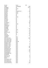
TYPICAL CHARACTERISTICS - Adronic Components GmbH
TYPICAL CHARACTERISTICS - Adronic Components GmbH
TYPICAL CHARACTERISTICS - Adronic Components GmbH

Create successful ePaper yourself
Turn your PDF publications into a flip-book with our unique Google optimized e-Paper software.
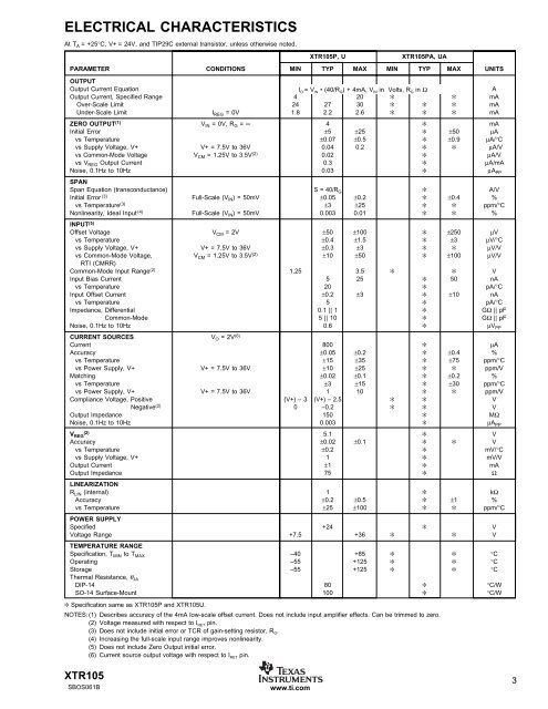
ELECTRICAL <strong>CHARACTERISTICS</strong><br />
At TA = +25°C, V+ = 24V, and TIP29C external transistor, unless otherwise noted.<br />
XTR105P, U XTR105PA, UA<br />
PARAMETER<br />
OUTPUT<br />
CONDITIONS MIN TYP MAX MIN TYP MAX UNITS<br />
Output Current Equation<br />
Output Current, Specified Range 4 20 ✻ ✻<br />
A<br />
mA<br />
Over-Scale Limit 24 27 30 ✻ ✻ ✻ mA<br />
Under-Scale Limit IREG = 0V 1.8 2.2 2.6 ✻ ✻ ✻ mA<br />
ZERO OUTPUT (1) VIN = 0V, RG = ∞ 4 ✻ mA<br />
Initial Error ±5 ±25 ✻ ±50 µA<br />
vs Temperature ±0.07 ±0.5 ✻ ±0.9 µA/°C<br />
vs Supply Voltage, V+ V+ = 7.5V to 36V 0.04 0.2 ✻ ✻ µA/V<br />
vs Common-Mode Voltage VCM = 1.25V to 3.5V (2) IO = VIN • (40/RG) + 4mA, VIN in Volts, RG in Ω<br />
0.02 ✻ µA/V<br />
vs VREG Output Current 0.3 ✻ µA/mA<br />
Noise, 0.1Hz to 10Hz 0.03 ✻ µAPP SPAN<br />
Span Equation (transconductance) S = 40/RG ✻ A/V<br />
Initial Error (3) Full-Scale (VIN) = 50mV ±0.05 ±0.2 ✻ ±0.4 %<br />
vs Temperature (3) ±3 ±25 ✻ ✻ ppm/°C<br />
Nonlinearity, Ideal Input (4) INPUT<br />
Full-Scale (VIN) = 50mV 0.003 0.01 ✻ ✻ %<br />
(5)<br />
Offset Voltage<br />
vs Temperature<br />
VCM = 2V ±50<br />
±0.4<br />
±100<br />
±1.5<br />
✻<br />
✻<br />
±250<br />
±3<br />
µV<br />
µV/°C<br />
vs Supply Voltage, V+ V+ = 7.5V to 36V ±0.3 ±3 ✻ ✻ µV/V<br />
vs Common-Mode Voltage, VCM = 1.25V to 3.5V (2) RTI (CMRR)<br />
±10 ±50 ✻ ±100 µV/V<br />
Common-Mode Input Range (2) 1.25 3.5 ✻ ✻ V<br />
Input Bias Current 5 25 ✻ 50 nA<br />
vs Temperature 20 ✻ pA/°C<br />
Input Offset Current ±0.2 ±3 ✻ ±10 nA<br />
vs Temperature 5 ✻ pA/°C<br />
Impedance, Differential 0.1 || 1 ✻ GΩ || pF<br />
Common-Mode 5 || 10 ✻ GΩ || pF<br />
Noise, 0.1Hz to 10Hz 0.6 ✻ µVPP CURRENT SOURCES V O = 2V (6)<br />
Current 800 ✻ µA<br />
Accuracy ±0.05 ±0.2 ✻ ±0.4 %<br />
vs Temperature ±15 ±35 ✻ ±75 ppm/°C<br />
vs Power Supply, V+ V+ = 7.5V to 36V ±10 ±25 ✻ ✻ ppm/V<br />
Matching ±0.02 ±0.1 ✻ ±0.2 %<br />
vs Temperature ±3 ±15 ✻ ±30 ppm/°C<br />
vs Power Supply, V+ V+ = 7.5V to 36V 1 10 ✻ ✻ ppm/V<br />
Compliance Voltage, Positive (V+) – 3 (V+) – 2.5 ✻ ✻ V<br />
Negative (2) 0 –0.2 ✻ ✻ V<br />
Output Impedance 150 ✻ MΩ<br />
Noise, 0.1Hz to 10Hz 0.003 ✻ µA PP<br />
V (2)<br />
REG 5.1 ✻ V<br />
Accuracy ±0.02 ±0.1 ✻ ✻ V<br />
vs Temperature ±0.2 ✻ mV/°C<br />
vs Supply Voltage, V+ 1 ✻ mV/V<br />
Output Current ±1 ✻ mA<br />
Output Impedance<br />
LINEARIZATION<br />
75 ✻ Ω<br />
RLIN (internal) 1 ✻ kΩ<br />
Accuracy ±0.2 ±0.5 ✻ ±1 %<br />
vs Temperature<br />
POWER SUPPLY<br />
±25 ±100 ✻ ✻ ppm/°C<br />
Specified +24 ✻ V<br />
Voltage Range<br />
TEMPERATURE RANGE<br />
+7.5 +36 ✻ ✻ V<br />
Specification, TMIN to TMAX –40 +85 ✻ ✻ °C<br />
Operating –55 +125 ✻ ✻ °C<br />
Storage<br />
Thermal Resistance, θJA –55 +125 ✻ ✻ °C<br />
DIP-14 80 ✻ °C/W<br />
SO-14 Surface-Mount 100 ✻ °C/W<br />
✻ Specification same as XTR105P and XTR105U.<br />
NOTES: (1) Describes accuracy of the 4mA low-scale offset current. Does not include input amplifier effects. Can be trimmed to zero.<br />
(2) Voltage measured with respect to IRET pin.<br />
(3) Does not include initial error or TCR of gain-setting resistor, RG. (4) Increasing the full-scale input range improves nonlinearity.<br />
(5) Does not include Zero Output initial error.<br />
(6) Current source output voltage with respect to IRET pin.<br />
XTR105 3<br />
SBOS061B www.ti.com