Backdrilling Signal Integrity - Sanmina-SCI
Backdrilling Signal Integrity - Sanmina-SCI
Backdrilling Signal Integrity - Sanmina-SCI

Create successful ePaper yourself
Turn your PDF publications into a flip-book with our unique Google optimized e-Paper software.
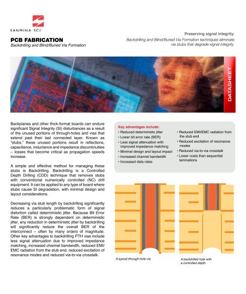
PCB FABRICATION<br />
<strong>Backdrilling</strong> and Blind/Buried Via Formation<br />
Backplanes and other thick-format boards can endure<br />
significant <strong>Signal</strong> <strong>Integrity</strong> (SI) disturbances as a result<br />
of the unused portions of through-holes and vias that<br />
extend past their last connected layer. Known as<br />
“stubs,” these unused portions result in reflections,<br />
capacitance, inductance and impedance discontinuities<br />
– losses that become critical as propagation speeds<br />
increase.<br />
A simple and effective method for managing these<br />
stubs is <strong>Backdrilling</strong>. <strong>Backdrilling</strong> is a Controlled<br />
Depth Drilling (CDD) technique that removes stubs<br />
with conventional numerically controlled (NC) drill<br />
equipment. It can be applied to any type of board where<br />
stubs cause SI degradation, with minimal design and<br />
layout considerations.<br />
Decreasing via stub length by backdrilling significantly<br />
reduces a particularly problematic form of signal<br />
distortion called deterministic jitter. Because Bit Error<br />
Rate (BER) is strongly dependent on deterministic<br />
jitter, any reduction in deterministic jitter by backdrilling<br />
will significantly reduce the overall BER of the<br />
interconnect – often by many orders of magnitude.<br />
Other key advantages to backdrilling PTH vias include<br />
less signal attenuation due to improved impedance<br />
matching, increased channel bandwidth, reduced EMI/<br />
EMC radiation from the stub end, reduced excitation of<br />
resonance modes and reduced via-to-via crosstalk.<br />
Preserving signal integrity.<br />
<strong>Backdrilling</strong> and Blind/Buried Via Formation techniques eliminate<br />
via stubs that degrade signal integrity.<br />
Key advantages include:<br />
• Reduced deterministic jitter<br />
• Lower bit error rate (BER)<br />
• Less signal attenuation with<br />
improved impedance matching<br />
• Minimal design and layout impact<br />
• Increased channel bandwidth<br />
• Increased data rates<br />
• Reduced EMI/EMC radiation from<br />
the stub end<br />
• Reduced excitation of resonance<br />
modes<br />
• Reduced via-to-via crosstalk<br />
• Lower costs than sequential<br />
laminations<br />
A typical through-hole via A backdrilled hole with<br />
a controlled depth
A second CDD technique for managing stubs is<br />
the formation of plated blind vias which prevent<br />
stubs from forming altogether. Blind Via Formation<br />
is possible at a much lower cost than multiple<br />
laminated build-up methods and achieves many<br />
of the same SI benefits.<br />
Blind Via Formation is limited by the throw of<br />
copper-plating baths to a maximum aspect ratio of<br />
1:1. However, it can be used in conjunction with<br />
<strong>Backdrilling</strong> in thicker board types for more complete<br />
stub management, or even by itself in thinner<br />
board types where a 1:1 aspect ratio is sufficient<br />
to eliminate the desired degree and percentage of<br />
stubs. This method produces the same improvement<br />
in SI as <strong>Backdrilling</strong> where similar lengths of<br />
stub are eliminated.<br />
As one the world’s largest manufacturers of hightechnology<br />
PCBs, <strong>Sanmina</strong>-<strong>SCI</strong> ® has significant<br />
experience in the design and production of boards<br />
using <strong>Backdrilling</strong> and/or CDD blind vias. We offer<br />
these capabilities throughout our fabrication<br />
sites in the United States and worldwide, providing<br />
design for manufacturability (DFM) support for<br />
our customers in pre-design and layout phases to<br />
ensure a smooth integration of these technologies<br />
to the production process.<br />
Improved frequency as a result of <strong>Backdrilling</strong> techniques<br />
Controlled Depth Drilling<br />
About <strong>Sanmina</strong>-<strong>SCI</strong><br />
<strong>Sanmina</strong>-<strong>SCI</strong> Corporation is a leading electronics contract manufacturer serving the fastest-growing segments of<br />
the global Electronics Manufacturing Services (EMS) market. Recognized as a technology leader, <strong>Sanmina</strong>-<strong>SCI</strong><br />
provides end-to-end manufacturing solutions, delivering unsurpassed quality and support to OEMs primarily in the<br />
communications, defense and aerospace, industrial and semiconductor, medical, multimedia, enterprise computing and<br />
storage, automotive technology and renewable energy sectors. <strong>Sanmina</strong>-<strong>SCI</strong> has facilities strategically located in key<br />
regions throughout the world. More information regarding the company is available at http://www.sanmina-sci.com.<br />
©2010 <strong>Sanmina</strong>-<strong>SCI</strong> Corporation, printed in U.S.A. <strong>Sanmina</strong>-<strong>SCI</strong> ® is a trademark or registered trademark in the U.S. and/or other jurisdictions of <strong>Sanmina</strong>-<strong>SCI</strong> Corporation.<br />
All trademarks and registered trademarks are the property of their respective owners. 0110<br />
2700 North First Street<br />
San Jose, California 95134<br />
Phone: +1 408 964 3555<br />
Fax: +1 408 964 3636<br />
Europe & Middle East<br />
+49 711 7287 220<br />
Asia Pacific<br />
+65 62457300<br />
For more information, please visit our website at www.sanmina-sci.com or send an email to info@sanmina-sci.com.