
You also want an ePaper? Increase the reach of your titles
YUMPU automatically turns print PDFs into web optimized ePapers that Google loves.
Bidirectional Voltage Translator<br />
5.5 V on A Port and 2.7 V to 3.6 V on B Port<br />
Control Inputs V IH/V IL Levels Are<br />
Referenced to V CCA Voltage<br />
Latch-Up Performance Exceeds 250 mA Per<br />
JESD 17<br />
ESD Protection Exceeds JESD 22<br />
− 2000-V Human-Body Model (A114-A)<br />
− 200-V Machine Model (A115-A)<br />
− 1000-V Charged-Device Model (C101)<br />
description/ordering information<br />
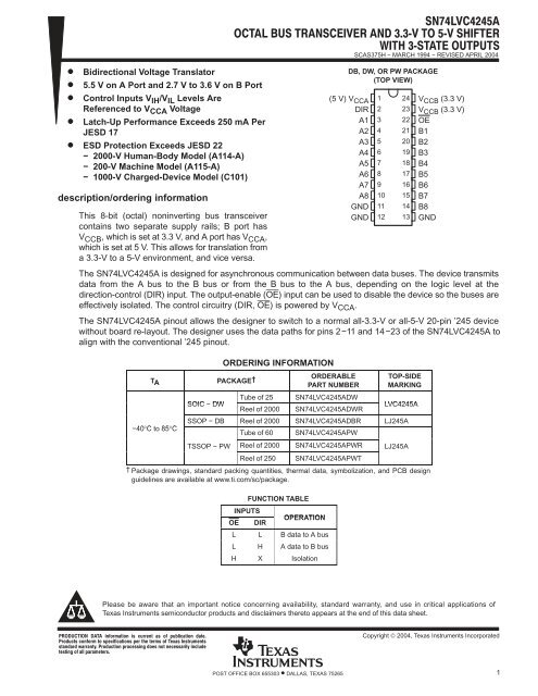
This 8-bit (octal) noninverting bus transceiver<br />
contains two separate supply rails; B port has<br />
V CCB, which is set at 3.3 V, and A port has V CCA,<br />
which is set at 5 V. This allows for translation from<br />
a 3.3-V to a 5-V environment, and vice versa.<br />
<br />
<br />
<br />
SCAS375H − MARCH 1994 − REVISED APRIL 2004<br />
The <strong>SN74LVC4245A</strong> is designed for asynchronous communication between data buses. The device transmits<br />
data from the A bus to the B bus or from the B bus to the A bus, depending on the logic level at the<br />
direction-control (DIR) input. The output-enable (OE) input can be used to disable the device so the buses are<br />
effectively isolated. The control circuitry (DIR, OE) is powered by VCCA. The <strong>SN74LVC4245A</strong> pinout allows the designer to switch to a normal all-3.3-V or all-5-V 20-pin ’245 device<br />
without board re-layout. The designer uses the data paths for pins 2−11 and 14−23 of the <strong>SN74LVC4245A</strong> to<br />
align with the conventional ’245 pinout.<br />
TA<br />
−40°C to 85°C<br />
ORDERING INFORMATION<br />
PACKAGE†<br />
ORDERABLE<br />
PART NUMBER<br />
SOIC − DW<br />
Tube of 25<br />
Reel of 2000<br />
<strong>SN74LVC4245A</strong>DW<br />
<strong>SN74LVC4245A</strong>DWR<br />
POST OFFICE BOX 655303 • DALLAS, TEXAS 75265<br />
TOP-SIDE<br />
MARKING<br />
LVC4245A<br />
SSOP − <strong>DB</strong> Reel of 2000 <strong>SN74LVC4245A</strong><strong>DB</strong>R LJ245A<br />
Tube of 60 <strong>SN74LVC4245A</strong>PW<br />
TSSOP − PW Reel of 2000 <strong>SN74LVC4245A</strong>PWR LJ245A<br />
Reel of 250 <strong>SN74LVC4245A</strong>PWT<br />
† Package drawings, standard packing quantities, thermal data, symbolization, and PCB design<br />
guidelines are available at www.ti.com/sc/package.<br />
FUNCTION TABLE<br />
INPUTS<br />
OE DIR<br />
OPERATION<br />
L L B data to A bus<br />
L H A data to B bus<br />
H X Isolation<br />
Please be aware that an important notice concerning availability, standard warranty, and use in critical applications of<br />
Texas Instruments semiconductor products and disclaimers thereto appears at the end of this data sheet.<br />
<br />
<br />
<br />
<br />
<strong>DB</strong>, DW, OR PW PACKAGE<br />
(TOP VIEW)<br />
(5 V) V CCA<br />
DIR<br />
A1<br />
A2<br />
A3<br />
A4<br />
A5<br />
A6<br />
A7<br />
A8<br />
GND<br />
GND<br />
1<br />
2<br />
3<br />
4<br />
5<br />
6<br />
7<br />
8<br />
9<br />
10<br />
11<br />
12<br />
24<br />
23<br />
22<br />
21<br />
20<br />
19<br />
18<br />
17<br />
16<br />
15<br />
14<br />
13<br />
V CCB (3.3 V)<br />
V CCB (3.3 V)<br />
OE<br />
B1<br />
B2<br />
B3<br />
B4<br />
B5<br />
B6<br />
B7<br />
B8<br />
GND<br />
Copyright © 2004, Texas Instruments Incorporated<br />
1
SCAS375H − MARCH 1994 − REVISED APRIL 2004<br />
logic diagram (positive logic)<br />
DIR<br />
A1<br />
To Seven Other Channels<br />
2 POST OFFICE BOX 655303 • DALLAS, TEXAS 75265<br />
2<br />
3<br />
absolute maximum ratings over operating free-air temperature range for V CCA = 4.5 V to 5.5 V<br />
(unless otherwise noted) †<br />
Supply voltage range, VCCA . . . . . . . . . . . . . . . . . . . . . . . . . . . . . . . . . . . . . . . . . . . . . . . . . . . . . . . . −0.5 V to 6.5 V<br />
Input voltage range, VI: A port (see Note 1) . . . . . . . . . . . . . . . . . . . . . . . . . . . . . . . . . . . −0.5 V to VCCA + 0.5 V<br />
Control inputs . . . . . . . . . . . . . . . . . . . . . . . . . . . . . . . . . . . . . . . . . . . . . . . . −0.5 V to 6 V<br />
Output voltage range, VO: A port (see Note 1) . . . . . . . . . . . . . . . . . . . . . . . . . . . . . . . . −0.5 V to VCCA + 0.5 V<br />
Input clamp current, IIK (VI < 0) . . . . . . . . . . . . . . . . . . . . . . . . . . . . . . . . . . . . . . . . . . . . . . . . . . . . . . . . . . . −50 mA<br />
Output clamp current, IOK (VO < 0) . . . . . . . . . . . . . . . . . . . . . . . . . . . . . . . . . . . . . . . . . . . . . . . . . . . . . . . . −50 mA<br />
Continuous output current, IO . . . . . . . . . . . . . . . . . . . . . . . . . . . . . . . . . . . . . . . . . . . . . . . . . . . . . . . . . . . . . ±50 mA<br />
Continuous current through each VCCA or GND . . . . . . . . . . . . . . . . . . . . . . . . . . . . . . . . . . . . . . . . . . . ±100 mA<br />
Package thermal impedance, θJA (see Note 2): <strong>DB</strong> package . . . . . . . . . . . . . . . . . . . . . . . . . . . . . . . . . 63°C/W<br />
DW package . . . . . . . . . . . . . . . . . . . . . . . . . . . . . . . . . 46°C/W<br />
PW package . . . . . . . . . . . . . . . . . . . . . . . . . . . . . . . . . 88°C/W<br />
Storage temperature range, Tstg . . . . . . . . . . . . . . . . . . . . . . . . . . . . . . . . . . . . . . . . . . . . . . . . . . . −65°C to 150°C<br />
† Stresses beyond those listed under “absolute maximum ratings” may cause permanent damage to the device. These are stress ratings only, and<br />
functional operation of the device at these or any other conditions beyond those indicated under “recommended operating conditions” is not<br />
implied. Exposure to absolute-maximum-rated conditions for extended periods may affect device reliability.<br />
NOTES: 1. This value is limited to 6 V maximum.<br />
2. The package thermal impedance is calculated in accordance with JESD 51-7.<br />
22<br />
21<br />
OE<br />
B1
SCAS375H − MARCH 1994 − REVISED APRIL 2004<br />
absolute maximum ratings over operating free-air temperature range for V CCB = 2.7 V to 3.6 V<br />
(unless otherwise noted) †<br />
Supply voltage range, VCCB . . . . . . . . . . . . . . . . . . . . . . . . . . . . . . . . . . . . . . . . . . . . . . . . . . . . . . . . −0.5 V to 4.6 V<br />
Input voltage range, VI: B port (see Note 3) . . . . . . . . . . . . . . . . . . . . . . . . . . . . . . . . . . . −0.5 V to VCCB + 0.5 V<br />
Output voltage range, VO: B port (see Note 3) . . . . . . . . . . . . . . . . . . . . . . . . . . . . . . . . −0.5 V to VCCB + 0.5 V<br />
Input clamp current, IIK (VI < 0) . . . . . . . . . . . . . . . . . . . . . . . . . . . . . . . . . . . . . . . . . . . . . . . . . . . . . . . . . . . −50 mA<br />
Output clamp current, IOK (VO < 0) . . . . . . . . . . . . . . . . . . . . . . . . . . . . . . . . . . . . . . . . . . . . . . . . . . . . . . . . −50 mA<br />
Continuous output current, IO . . . . . . . . . . . . . . . . . . . . . . . . . . . . . . . . . . . . . . . . . . . . . . . . . . . . . . . . . . . . . ±50 mA<br />
Continuous current through VCCB or GND . . . . . . . . . . . . . . . . . . . . . . . . . . . . . . . . . . . . . . . . . . . . . . . . ±100 mA<br />
Package thermal impedance, θJA (see Note 2): <strong>DB</strong> package . . . . . . . . . . . . . . . . . . . . . . . . . . . . . . . . . 63°C/W<br />
DW package . . . . . . . . . . . . . . . . . . . . . . . . . . . . . . . . . 46°C/W<br />
PW package . . . . . . . . . . . . . . . . . . . . . . . . . . . . . . . . . 88°C/W<br />
Storage temperature range, Tstg . . . . . . . . . . . . . . . . . . . . . . . . . . . . . . . . . . . . . . . . . . . . . . . . . . . −65°C to 150°C<br />
† Stresses beyond those listed under “absolute maximum ratings” may cause permanent damage to the device. These are stress ratings only, and<br />
functional operation of the device at these or any other conditions beyond those indicated under “recommended operating conditions” is not<br />
implied. Exposure to absolute-maximum-rated conditions for extended periods may affect device reliability.<br />
NOTES: 2. The package thermal impedance is calculated in accordance with JESD 51-7.<br />
3. This value is limited to 4.6 V maximum.<br />
recommended operating conditions for V CCA = 4.5 V to 5.5 V (see Note 4)<br />
MIN MAX UNIT<br />
VCCA Supply voltage 4.5 5.5 V<br />
VIH High-level input voltage 2 V<br />
VIL Low-level input voltage 0.8 V<br />
VIA Input voltage 0 VCCA V<br />
VOA Output voltage 0 VCCA V<br />
IOH High-level output current −24 mA<br />
IOL Low-level output current 24 mA<br />
TA Operating free-air temperature −40 85 °C<br />
NOTE 4: All unused inputs of the device must be held at the associated VCC or GND to ensure proper device operation. Refer to the TI application<br />
report, Implications of Slow or Floating CMOS Inputs, literature number SCBA004.<br />
recommended operating conditions for V CCB = 2.7 V to 3.6 V (see Note 4)<br />
POST OFFICE BOX 655303 • DALLAS, TEXAS 75265<br />
MIN MAX UNIT<br />
VCCB Supply voltage 2.7 3.6 V<br />
VIH High-level input voltage VCCB = 2.7 V to 3.6 V 2 V<br />
VIL Low-level input voltage VCCB = 2.7 V to 3.6 V 0.8 V<br />
VIB Input voltage 0 VCCB V<br />
VOB Output voltage 0 VCCB V<br />
IOH IOH<br />
IOL IOL<br />
High-level output current current<br />
Low-level output current<br />
VCCB = 2.7 V −12<br />
VCCB = 3 V −24<br />
VCCB = 2.7 V 12<br />
VCCB = 3 V 24<br />
TA Operating free-air temperature −40 85 °C<br />
NOTE 4: All unused inputs of the device must be held at the associated VCC or GND to ensure proper device operation. Refer to the TI application<br />
report, Implications of Slow or Floating CMOS Inputs, literature number SCBA004.<br />
mA<br />
mA<br />
3
SCAS375H − MARCH 1994 − REVISED APRIL 2004<br />
electrical characteristics over recommended operating free-air temperature range for<br />
V CCA = 4.5 V to 5.5 V (unless otherwise noted) (see Note 5)<br />
VOH VOH<br />
VOL VOL<br />
PARAMETER TEST CONDITIONS VCCA MIN TYP† MAX UNIT<br />
IOH IOH = −100 µA A<br />
IOH IOH = −24 mA<br />
IOL IOL = 100 µAA<br />
IOL IOL = 24 mA<br />
4 POST OFFICE BOX 655303 • DALLAS, TEXAS 75265<br />
4.5 V 4.3<br />
5.5 V 5.3<br />
4.5 V 3.7<br />
5.5 V 4.7<br />
4.5 V 0.2<br />
5.5 V 0.2<br />
4.5 V 0.55<br />
5.5 V 0.55<br />
II Control inputs VI = VCCA or GND 5.5 V ±1 µA<br />
IOZ ‡ A port VO = VCCA or GND 5.5 V ±5 µA<br />
ICCA VI = VCCA or GND, IO = 0 5.5 V 80 µA<br />
∆ICCA § One input at 3.4 V, Other inputs at VCCA or GND 5.5 V 1.5 mA<br />
Ci Control inputs VI = VCCA or GND Open 5 pF<br />
Cio A port VO = VCCA or GND 5 V 11 pF<br />
† All typical values are measured at VCC = 5 V, TA = 25°C.<br />
‡ For I/O ports, the parameter IOZ includes the input leakage current.<br />
§ This is the increase in supply current for each input that is at one of the specified TTL voltage levels, rather than 0 V or the associated VCC.<br />
NOTE 5: VCCB = 2.7 V to 3.6 V<br />
electrical characteristics over recommended operating free-air temperature range for<br />
V CCB = 2.7 V to 3.6 V (unless otherwise noted) (see Note 6)<br />
PARAMETER TEST CONDITIONS VCCB MIN TYP MAX UNIT<br />
VOH VOH<br />
IOH = −100 µA 2.7 V to 3.6 V VCC−0.2<br />
IOH IOH = −12 mA<br />
2.7 V 2.2<br />
3 V 2.4<br />
IOH = −24 mA 3 V 2<br />
IOL = 100 µA 2.7 V to 3.6 V 0.2<br />
VOL VOL<br />
IOL = 12 mA 2.7 V 0.4 V<br />
IOL = 24 mA 3 V 0.55<br />
IOZ ‡ B port VO = VCCB or GND 3.6 V ±5 µA<br />
ICCB VI = VCCB or GND, IO = 0 3.6 V 50 µA<br />
∆ICCB § One input at VCCB − 0.6 V, Other inputs at VCCB or GND 2.7 V to 3.6 V 0.5 mA<br />
Cio B port VO = VCCB or GND 3.3 V 11 pF<br />
‡ For I/O ports, the parameter IOZ includes the input leakage current.<br />
§ This is the increase in supply current for each input that is at one of the specified TTL voltage levels, rather than 0 V or the associated VCC.<br />
All typical values are measured at VCC = 3.3 V, TA = 25°C.<br />
NOTE 6: VCCA = 5 V ± 0.5 V<br />
V<br />
V<br />
V
SCAS375H − MARCH 1994 − REVISED APRIL 2004<br />
switching characteristics over recommended operating free-air temperature range, C L = 50 pF<br />
(unless otherwise noted) (see Figures 1 and 2)<br />
PARAMETER<br />
tPHL<br />
tPLH<br />
tPHL<br />
tPLH<br />
tPZL<br />
tPZH<br />
tPZL<br />
tPZH<br />
tPLZ<br />
tPHZ<br />
tPLZ<br />
tPHZ<br />
FROM<br />
TO<br />
(INPUT) (OUTPUT)<br />
A B<br />
B A<br />
OE A<br />
OE OE B<br />
OE A<br />
OE B<br />
operating characteristics, V CCA = 4.5 V to 5.5 V, V CCB = 2.7 V to 3.6 V, T A = 25°C<br />
Cpd Cpd<br />
Power dissipation capacitance per transceiver<br />
power-up considerations †<br />
POST OFFICE BOX 655303 • DALLAS, TEXAS 75265<br />
VCCA = 5 V ± 0.5 V,<br />
VCCB = 2.7 V TO 3.6 V UNIT<br />
MIN MAX<br />
1 6.3<br />
1 6.7<br />
1 6.1<br />
1 5<br />
1 9<br />
1 8.1<br />
1 8.8<br />
1 9.8<br />
1 7<br />
1 5.8<br />
1 7.7<br />
1 7.8<br />
PARAMETER TEST CONDITIONS TYP UNIT<br />
Outputs enabled<br />
Outputs disabled<br />
CL CL = 0, f = 10 MHz<br />
TI level-translation devices offer an opportunity for successful mixed-voltage signal design. A proper power-up<br />
sequence always should be followed to avoid excessive supply current, bus contention, oscillations, or other<br />
anomalies caused by improperly biased device pins. Take these precautions to guard against such power-up<br />
problems:<br />
1. Connect ground before any supply voltage is applied.<br />
2. Power up the control side of the device (VCCA for all four of these devices).<br />
3. Tie OE to VCCA with a pullup resistor so that it ramps with VCCA. 4. Depending on the direction of the data path, DIR can be high or low. If DIR high is needed (A data to B bus),<br />
ramp it with VCCA. Otherwise, keep DIR low.<br />
† Refer to the TI application report, Texas Instruments Voltage-Level-Translation Devices, literature number SCEA021.<br />
39.5<br />
5<br />
ns<br />
ns<br />
ns<br />
ns<br />
ns<br />
ns<br />
pF<br />
5
SCAS375H − MARCH 1994 − REVISED APRIL 2004<br />
From Output<br />
Under Test<br />
CL = 50 pF<br />
(see Note A)<br />
Input<br />
Input<br />
Output<br />
tPLH<br />
50% VCC<br />
1.5 V<br />
PARAMETER MEASUREMENT INFORMATION<br />
A PORT<br />
500 Ω<br />
500 Ω<br />
LOAD CIRCUIT<br />
tw<br />
1.5 V 1.5 V<br />
VOLTAGE WAVEFORMS<br />
PULSE DURATION<br />
50% VCC<br />
1.5 V<br />
VOLTAGE WAVEFORMS<br />
PROPAGATION DELAY TIMES<br />
NONINVERTING OUTPUTS<br />
6 POST OFFICE BOX 655303 • DALLAS, TEXAS 75265<br />
S1<br />
VCC<br />
0 V<br />
tPHL<br />
VOH<br />
VOL<br />
2 × VCC<br />
Open<br />
GND<br />
VCC<br />
0 V<br />
Output<br />
Control<br />
Output<br />
Waveform 1<br />
S1 at 2 × VCC<br />
(see Note B)<br />
Output<br />
Waveform 2<br />
S1 at GND<br />
(see Note B)<br />
tPZL<br />
tPZH<br />
TEST S1<br />
tPLH/tPHL<br />
tPLZ/tPZL<br />
tPHZ/tPZH<br />
50% VCC<br />
50% VCC<br />
1.5 V<br />
Open<br />
2 × VCC<br />
GND<br />
1.5 V<br />
tPLZ<br />
VOL + 0.3 V<br />
VOL<br />
tPHZ<br />
3 V<br />
0 V<br />
VCC<br />
VOH<br />
VOH − 0.3 V<br />
≈0 V<br />
VOLTAGE WAVEFORMS<br />
ENABLE AND DISABLE TIMES<br />
LOW- AND HIGH-LEVEL ENABLING<br />
NOTES: A. CL includes probe and jig capacitance.<br />
B. Waveform 1 is for an output with internal conditions such that the output is low, except when disabled by the output control.<br />
Waveform 2 is for an output with internal conditions such that the output is high, except when disabled by the output control.<br />
C. All input pulses are supplied by generators having the following characteristics: PRR ≤ 10 MHz, ZO = 50 Ω, tr ≤ 2.5 ns, tf ≤ 2.5 ns.<br />
D. The outputs are measured one at a time, with one transition per measurement.<br />
E. All parameters and waveforms are not applicable to all devices.<br />
Figure 1. Load Circuit and Voltage Waveforms
From Output<br />
Under Test<br />
CL = 50 pF<br />
(see Note A)<br />
Input<br />
Output<br />
tPLH<br />
<br />
<br />
<br />
SCAS375H − MARCH 1994 − REVISED APRIL 2004<br />
PARAMETER MEASUREMENT INFORMATION<br />
B PORT<br />
500 Ω<br />
500 Ω<br />
LOAD CIRCUIT<br />
tw<br />
1.5 V 1.5 V<br />
VOLTAGE WAVEFORMS<br />
PULSE DURATION<br />
Input 1.5 V 1.5 V<br />
VOLTAGE WAVEFORMS<br />
PROPAGATION DELAY TIMES<br />
NONINVERTING OUTPUTS<br />
S1<br />
3 V<br />
0 V<br />
7 V<br />
tPHL<br />
VOH<br />
1.5 V 1.5 V<br />
VOL<br />
Open<br />
GND<br />
3 V<br />
0 V<br />
Output<br />
Control<br />
Output<br />
Waveform 1<br />
S1 at 7 V<br />
(see Note B)<br />
Output<br />
Waveform 2<br />
S1 at GND<br />
(see Note B)<br />
tPZL<br />
tPZH<br />
POST OFFICE BOX 655303 • DALLAS, TEXAS 75265<br />
TEST S1<br />
tPLH/tPHL<br />
tPLZ/tPZL<br />
tPHZ/tPZH<br />
1.5 V<br />
Open<br />
7 V<br />
GND<br />
1.5 V<br />
tPLZ<br />
VOL + 0.3 V<br />
VOL<br />
tPHZ<br />
3 V<br />
0 V<br />
3.5 V<br />
VOH<br />
VOH − 0.3 V<br />
≈0 V<br />
VOLTAGE WAVEFORMS<br />
ENABLE AND DISABLE TIMES<br />
LOW- AND HIGH-LEVEL ENABLING<br />
NOTES: A. CL includes probe and jig capacitance.<br />
B. Waveform 1 is for an output with internal conditions such that the output is low, except when disabled by the output control.<br />
Waveform 2 is for an output with internal conditions such that the output is high, except when disabled by the output control.<br />
C. All input pulses are supplied by generators having the following characteristics: PRR ≤ 10 MHz, ZO = 50 Ω, tr ≤ 2.5 ns, tf ≤ 2.5 ns.<br />
D. The outputs are measured one at a time, with one transition per measurement.<br />
E. All parameters and waveforms are not applicable to all devices.<br />
Figure 2. Load Circuit and Voltage Waveforms<br />
1.5 V<br />
1.5 V<br />
7
POST OFFICE BOX 655303 • DALLAS, TEXAS 75265<br />
MECHANICAL DATA<br />
MSOI003E – JANUARY 1995 – REVISED SEPTEMBER 2001<br />
DW (R-PDSO-G**) PLASTIC SMALL-OUTLINE PACKAGE<br />
16 PINS SHOWN<br />
0.050 (1,27)<br />
16<br />
1<br />
0.104 (2,65) MAX<br />
A<br />
DIM<br />
0.020 (0,51)<br />
0.014 (0,35)<br />
9<br />
8<br />
0.012 (0,30)<br />
0.004 (0,10)<br />
PINS **<br />
A MAX<br />
A MIN<br />
0.419 (10,65)<br />
0.400 (10,15)<br />
0.299 (7,59)<br />
0.291 (7,39)<br />
16<br />
0.410 0.462<br />
(10,41) (11,73)<br />
0.400<br />
(10,16)<br />
0.010 (0,25)<br />
Seating Plane<br />
0.004 (0,10)<br />
18<br />
0.453<br />
(11,51)<br />
0.510<br />
(12,95)<br />
0.500<br />
(12,70)<br />
0.010 (0,25) NOM<br />
0°– 8°<br />
24<br />
0.610<br />
(15,49)<br />
0.600<br />
(15,24)<br />
NOTES: A. All linear dimensions are in inches (millimeters).<br />
B. This drawing is subject to change without notice.<br />
C. Body dimensions do not include mold flash or protrusion not to exceed 0.006 (0,15).<br />
D. Falls within JEDEC MS-013<br />
20<br />
Gage Plane<br />
28<br />
0.710<br />
(18,03)<br />
0.700<br />
(17,78)<br />
0.010 (0,25)<br />
0.050 (1,27)<br />
0.016 (0,40)<br />
4040000/E 08/01
POST OFFICE BOX 655303 • DALLAS, TEXAS 75265<br />
MECHANICAL DATA<br />
MSSO002E – JANUARY 1995 – REVISED DECEMBER 2001<br />
<strong>DB</strong> (R-PDSO-G**) PLASTIC SMALL-OUTLINE<br />
28 PINS SHOWN<br />
0,38<br />
0,65 0,15 M<br />
0,22<br />
28<br />
1<br />
2,00 MAX<br />
DIM<br />
A<br />
A MAX<br />
A MIN<br />
PINS **<br />
14<br />
6,50<br />
15<br />
14<br />
0,05 MIN<br />
5,60<br />
5,00<br />
8,20<br />
7,40<br />
Seating Plane<br />
24<br />
8,50<br />
7,90<br />
28<br />
10,50<br />
NOTES: A. All linear dimensions are in millimeters.<br />
B. This drawing is subject to change without notice.<br />
C. Body dimensions do not include mold flash or protrusion not to exceed 0,15.<br />
D. Falls within JEDEC MO-150<br />
5,90<br />
16<br />
6,50<br />
5,90<br />
20<br />
7,50<br />
6,90<br />
0,10<br />
9,90<br />
30<br />
10,50<br />
9,90<br />
0,25<br />
0,09<br />
0°–8°<br />
Gage Plane<br />
38<br />
12,90<br />
12,30<br />
0,25<br />
0,95<br />
0,55<br />
4040065 /E 12/01
POST OFFICE BOX 655303 • DALLAS, TEXAS 75265<br />
MECHANICAL DATA<br />
MTSS001C – JANUARY 1995 – REVISED FEBRUARY 1999<br />
PW (R-PDSO-G**) PLASTIC SMALL-OUTLINE PACKAGE<br />
14 PINS SHOWN<br />
0,65<br />
14<br />
1<br />
1,20 MAX<br />
A<br />
DIM<br />
A MAX<br />
A MIN<br />
7<br />
PINS **<br />
8<br />
0,15<br />
0,05<br />
0,30<br />
0,19<br />
8<br />
3,10<br />
2,90<br />
4,50<br />
4,30<br />
0,10<br />
6,60<br />
6,20<br />
M<br />
Seating Plane<br />
14<br />
5,10<br />
4,90<br />
0,10<br />
16<br />
5,10<br />
4,90<br />
20<br />
6,60<br />
6,40<br />
0,15 NOM<br />
0°–8°<br />
NOTES: A. All linear dimensions are in millimeters.<br />
B. This drawing is subject to change without notice.<br />
C. Body dimensions do not include mold flash or protrusion not to exceed 0,15.<br />
D. Falls within JEDEC MO-153<br />
24<br />
7,90<br />
7,70<br />
Gage Plane<br />
28<br />
9,80<br />
9,60<br />
0,25<br />
0,75<br />
0,50<br />
4040064/F 01/97
IMPORTANT NOTICE<br />
Texas Instruments Incorporated and its subsidiaries (TI) reserve the right to make corrections, modifications,<br />
enhancements, improvements, and other changes to its products and services at any time and to discontinue<br />
any product or service without notice. Customers should obtain the latest relevant information before placing<br />
orders and should verify that such information is current and complete. All products are sold subject to TI’s terms<br />
and conditions of sale supplied at the time of order acknowledgment.<br />
TI warrants performance of its hardware products to the specifications applicable at the time of sale in<br />
accordance with TI’s standard warranty. Testing and other quality control techniques are used to the extent TI<br />
deems necessary to support this warranty. Except where mandated by government requirements, testing of all<br />
parameters of each product is not necessarily performed.<br />
TI assumes no liability for applications assistance or customer product design. Customers are responsible for<br />
their products and applications using TI components. To minimize the risks associated with customer products<br />
and applications, customers should provide adequate design and operating safeguards.<br />
TI does not warrant or represent that any license, either express or implied, is granted under any TI patent right,<br />
copyright, mask work right, or other TI intellectual property right relating to any combination, machine, or process<br />
in which TI products or services are used. Information published by TI regarding third-party products or services<br />
does not constitute a license from TI to use such products or services or a warranty or endorsement thereof.<br />
Use of such information may require a license from a third party under the patents or other intellectual property<br />
of the third party, or a license from TI under the patents or other intellectual property of TI.<br />
Reproduction of information in TI data books or data sheets is permissible only if reproduction is without<br />
alteration and is accompanied by all associated warranties, conditions, limitations, and notices. Reproduction<br />
of this information with alteration is an unfair and deceptive business practice. TI is not responsible or liable for<br />
such altered documentation.<br />
Resale of TI products or services with statements different from or beyond the parameters stated by TI for that<br />
product or service voids all express and any implied warranties for the associated TI product or service and<br />
is an unfair and deceptive business practice. TI is not responsible or liable for any such statements.<br />
Following are URLs where you can obtain information on other Texas Instruments products and application<br />
solutions:<br />
Products Applications<br />
Amplifiers amplifier.ti.com Audio www.ti.com/audio<br />
Data Converters dataconverter.ti.com Automotive www.ti.com/automotive<br />
DSP dsp.ti.com Broadband www.ti.com/broadband<br />
Interface interface.ti.com Digital Control www.ti.com/digitalcontrol<br />
Logic logic.ti.com Military www.ti.com/military<br />
Power Mgmt power.ti.com Optical Networking www.ti.com/opticalnetwork<br />
Microcontrollers microcontroller.ti.com Security www.ti.com/security<br />
Telephony www.ti.com/telephony<br />
Video & Imaging www.ti.com/video<br />
Wireless www.ti.com/wireless<br />
Mailing Address: Texas Instruments<br />
Post Office Box 655303 Dallas, Texas 75265<br />
Copyright © 2004, Texas Instruments Incorporated