MAPS-010164 - M/A-COM Technology Solutions
MAPS-010164 - M/A-COM Technology Solutions
MAPS-010164 - M/A-COM Technology Solutions

Create successful ePaper yourself
Turn your PDF publications into a flip-book with our unique Google optimized e-Paper software.
1<br />
<strong>MAPS</strong>-<strong>010164</strong><br />
Digital Phase Shifter<br />
6-Bit, 2.3 - 3.8 GHz<br />
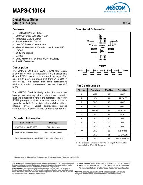
Features<br />
6 Bit Digital Phase Shifter<br />
360° Coverage with LSB = 5.6°<br />
Integrated CMOS Driver<br />
Serial or Parallel Control<br />
Low DC Power Consumption<br />
Minimal Attenuation Variation over Phase Shift<br />
Range<br />
50 Ω Impedance<br />
EAR99<br />
Lead-Free 4 mm 24-Lead PQFN Package<br />
RoHS* Compliant<br />
Description<br />
The <strong>MAPS</strong>-<strong>010164</strong> is a GaAs pHEMT 6-bit digital<br />
phase shifter with an integrated CMOS driver in a<br />
4 mm PQFN plastic surface mount package. Step<br />
size is 5.6° providing phase shift from 0° to 360° in<br />
5.6° steps. This design has been optimized to<br />
minimize variation in attenuation over the phase shift<br />
range.<br />
The <strong>MAPS</strong>-<strong>010164</strong> is ideally suited for use where<br />
high phase accuracy with minimum loss variation<br />
over the phase shift range are required. The 4 mm<br />
PQFN package provides a smaller footprint than is<br />
typically available for a digital phase shifter with an<br />
internal driver. Typical applications include<br />
communications antennas and phased array radars.<br />
Ordering Information 1<br />
Part Number Package<br />
<strong>MAPS</strong>-<strong>010164</strong>-TR0500 500 piece reel<br />
<strong>MAPS</strong>-<strong>010164</strong>-001SMB Sample Test Board<br />
1. Reference Application Note M513 for reel size information.<br />
* Restrictions on Hazardous Substances, European Union Directive 2002/95/EC.<br />
ADVANCED: Data Sheets contain information regarding a product M/A-<strong>COM</strong> <strong>Technology</strong> <strong>Solutions</strong><br />
is considering for development. Performance is based on target specifications, simulated results,<br />
and/or prototype measurements. Commitment to develop is not guaranteed.<br />
PRELIMINARY: Data Sheets contain information regarding a product M/A-<strong>COM</strong> <strong>Technology</strong><br />
<strong>Solutions</strong> has under development. Performance is based on engineering tests. Specifications are<br />
typical. Mechanical outline has been fixed. Engineering samples and/or test data may be available.<br />
Commitment to produce in volume is not guaranteed.<br />
Functional Schematic<br />
P/S<br />
Pin Configuration 2<br />
Rev. V3<br />
Pin No. Function Pin No. Function<br />
1 VEE 13 GND<br />
2 P/S 14 RF OUT<br />
3 GND 15 GND<br />
4 GND 16 GND<br />
5 RF IN 17 SER OUT<br />
6 GND 18 VCC<br />
7 GND 19 D6<br />
8 GND 20 D5<br />
9 GND 21 D4<br />
10 GND 22 D3 or LE<br />
11 GND 23 D2 or CLK<br />
12 GND 24 D1 or SER IN<br />
2. The exposed pad centered on the package bottom must be<br />
connected to RF and DC ground.<br />
• North America Tel: 800.366.2266 • Europe Tel: +353.21.244.6400<br />
• India Tel: +91.80.43537383 • China Tel: +86.21.2407.1588<br />
Visit www.macomtech.com for additional data sheets and product information.<br />
M/A-<strong>COM</strong> <strong>Technology</strong> <strong>Solutions</strong> Inc. and its affiliates reserve the right to make<br />
changes to the product(s) or information contained herein without notice.
2<br />
<strong>MAPS</strong>-<strong>010164</strong><br />
Digital Phase Shifter<br />
6-Bit, 2.3 - 3.8 GHz<br />
Electrical Specifications:<br />
Freq. = 2.3 - 3.8 GHz, TA = 25°C, Z0 = 50 Ω, VCC = +5.0 V, VEE = -5.0 V<br />
Parameter Test Conditions Units Min. Typ. Max.<br />
Operating Power 3 2.3 - 3.8 GHz dBm — — +25<br />
Insertion Loss<br />
(Any Phase State)<br />
Any Phase State dB — 3.2 4.5<br />
Attenuation Variation Across All Phase States dB — ± 0.6 —<br />
RMS Attenuation Error 4<br />
All Values Relative to Insertion Loss at<br />
Reference Phase<br />
ADVANCED: Data Sheets contain information regarding a product M/A-<strong>COM</strong> <strong>Technology</strong> <strong>Solutions</strong><br />
is considering for development. Performance is based on target specifications, simulated results,<br />
and/or prototype measurements. Commitment to develop is not guaranteed.<br />
PRELIMINARY: Data Sheets contain information regarding a product M/A-<strong>COM</strong> <strong>Technology</strong><br />
<strong>Solutions</strong> has under development. Performance is based on engineering tests. Specifications are<br />
typical. Mechanical outline has been fixed. Engineering samples and/or test data may be available.<br />
Commitment to produce in volume is not guaranteed.<br />
dB — 0.3 —<br />
RMS Phase Error 4 All Values Relative to Reference Phase deg — 3 —<br />
Phase Accuracy<br />
Relative to Reference Loss State<br />
VSWR<br />
5.6 Degree Bit<br />
11.2 Degree Bit<br />
22.5 Degree Bit<br />
45 Degree Bit<br />
90 Degree Bit<br />
180 Degree Bit<br />
Sum of All Bits<br />
RF IN<br />
RF OUT<br />
deg<br />
Ratio<br />
—<br />
—<br />
—<br />
—<br />
—<br />
—<br />
—-<br />
—<br />
—<br />
± 1.5<br />
± 1.5<br />
± 2<br />
± 2<br />
± 3<br />
± 4<br />
± 5<br />
1.3:1<br />
1.3:1<br />
1 dB Compression Reference State dBm — 25 —<br />
Input IP3 Two-tone inputs up to +5 dBm dBm — 45 —<br />
TRISE, TFALL 10% to 90% RF, 90% to 10% RF ns — 50 —<br />
VCC<br />
VEE<br />
VIL<br />
VIH<br />
—<br />
—<br />
LOW-level input voltage<br />
HIGH-level input voltage<br />
V<br />
V<br />
3.0<br />
-5.5<br />
0.0<br />
0.7 x VCC<br />
lIN (Input Control Current) VIN = VCC or GND µA — 1 —<br />
VOH<br />
VOL<br />
Icc<br />
(Quiescent Supply Current)<br />
IEE<br />
For serial out; IOH = -100 µA<br />
For serial out; IOL = 100 µA<br />
V<br />
VCC - 0.2<br />
—<br />
—<br />
-5.0<br />
—<br />
—<br />
—<br />
—<br />
Rev. V3<br />
• North America Tel: 800.366.2266 • Europe Tel: +353.21.244.6400<br />
• India Tel: +91.80.43537383 • China Tel: +86.21.2407.1588<br />
Visit www.macomtech.com for additional data sheets and product information.<br />
M/A-<strong>COM</strong> <strong>Technology</strong> <strong>Solutions</strong> Inc. and its affiliates reserve the right to make<br />
changes to the product(s) or information contained herein without notice.<br />
—<br />
—<br />
—<br />
—<br />
—<br />
—<br />
—<br />
—<br />
—<br />
5.5<br />
-3.0<br />
0.3 x VCC<br />
Vcntrl = VCC or GND µA — — 2.5<br />
VEE min to max<br />
Vin = VIL or VIH<br />
VCC<br />
—<br />
0.2<br />
mA -1.0 -0.1 —<br />
3. Maximum operating power is the maximum power where the specifications are guaranteed.<br />
4. RMS is calculated across all 63 amplitude or phase states relative to the amplitude or phase in the 0° phase state at a given frequency.
3<br />
<strong>MAPS</strong>-<strong>010164</strong><br />
Digital Phase Shifter<br />
6-Bit, 2.3 - 3.8 GHz<br />
Absolute Maximum Ratings 5,6<br />
Parameter Absolute Maximum<br />
Input Power<br />
2.3 - 3.8 GHz<br />
VCC<br />
VEE<br />
+27 dBm<br />
-0.5V ≤ VCC ≤ +7.0V<br />
-7.0V ≤ VEE ≤ +0.5V<br />
D1-D6, P/S, LE, CLK or<br />
SER IN<br />
-0.5V ≤ VIN ≤ VCC + 0.5V<br />
SER OUT -0.5V ≤ VOUT ≤ VCC + 0.5V<br />
Operating Temperature -40ºC to +85ºC<br />
Storage Temperature -65ºC to +150ºC<br />
5. Exceeding any one or combination of these limits may cause<br />
permanent damage to this device.<br />
6. M/A-<strong>COM</strong> <strong>Technology</strong> <strong>Solutions</strong> does not recommend<br />
sustained operation near these survivability limits.<br />
Handling Procedures<br />
Please observe the following precautions to avoid<br />
damage:<br />
Static Sensitivity<br />
Gallium Arsenide and Silicon Integrated Circuits<br />
are sensitive to electrostatic discharge (ESD) and<br />
can be damaged by static electricity. Proper ESD<br />
control techniques should be used when handling<br />
these devices.<br />
ADVANCED: Data Sheets contain information regarding a product M/A-<strong>COM</strong> <strong>Technology</strong> <strong>Solutions</strong><br />
is considering for development. Performance is based on target specifications, simulated results,<br />
and/or prototype measurements. Commitment to develop is not guaranteed.<br />
PRELIMINARY: Data Sheets contain information regarding a product M/A-<strong>COM</strong> <strong>Technology</strong><br />
<strong>Solutions</strong> has under development. Performance is based on engineering tests. Specifications are<br />
typical. Mechanical outline has been fixed. Engineering samples and/or test data may be available.<br />
Commitment to produce in volume is not guaranteed.<br />
Sample Board Header Pin Labels<br />
Rev. V3<br />
• North America Tel: 800.366.2266 • Europe Tel: +353.21.244.6400<br />
• India Tel: +91.80.43537383 • China Tel: +86.21.2407.1588<br />
Visit www.macomtech.com for additional data sheets and product information.<br />
M/A-<strong>COM</strong> <strong>Technology</strong> <strong>Solutions</strong> Inc. and its affiliates reserve the right to make<br />
changes to the product(s) or information contained herein without notice.
4<br />
<strong>MAPS</strong>-<strong>010164</strong><br />
Digital Phase Shifter<br />
6-Bit, 2.3 - 3.8 GHz<br />
Typical Performance Curves<br />
RFIN Return Loss vs. Frequency (All States) RFOUT Return Loss vs. Frequency (All States)<br />
-10<br />
-15<br />
-20<br />
-25<br />
-30<br />
-35<br />
-40<br />
-45<br />
-50<br />
2.2 2.4 2.6 2.8 3.0 3.2 3.4 3.6 3.8 4.0<br />
Frequency (GHz)<br />
Mean RMS Phase Error vs. Frequency Mean RMS Amplitude Error vs. Frequency<br />
10<br />
8<br />
6<br />
4<br />
2<br />
0<br />
2.2 2.4 2.6 2.8 3.0 3.2 3.4 3.6 3.8 4.0<br />
Frequency (GHz)<br />
Phase Error (degrees) vs. State Amplitude Error (dB) vs. State<br />
8<br />
4<br />
0<br />
-4<br />
-8<br />
2.3 GHz<br />
3.0 GHz<br />
3.8 GHz<br />
-12<br />
0 45 90 135 180<br />
State<br />
225 270 315 360<br />
ADVANCED: Data Sheets contain information regarding a product M/A-<strong>COM</strong> <strong>Technology</strong> <strong>Solutions</strong><br />
is considering for development. Performance is based on target specifications, simulated results,<br />
and/or prototype measurements. Commitment to develop is not guaranteed.<br />
PRELIMINARY: Data Sheets contain information regarding a product M/A-<strong>COM</strong> <strong>Technology</strong><br />
<strong>Solutions</strong> has under development. Performance is based on engineering tests. Specifications are<br />
typical. Mechanical outline has been fixed. Engineering samples and/or test data may be available.<br />
Commitment to produce in volume is not guaranteed.<br />
-10<br />
-15<br />
-20<br />
-25<br />
-30<br />
-35<br />
-40<br />
-45<br />
-50<br />
2.2 2.4 2.6 2.8 3.0 3.2 3.4 3.6 3.8 4.0<br />
0.6<br />
0.5<br />
0.4<br />
0.3<br />
0.2<br />
Frequency (GHz)<br />
0.1<br />
2.2 2.4 2.6 2.8 3.0 3.2 3.4 3.6 3.8 4.0<br />
Frequency (GHz)<br />
2.0<br />
1.5<br />
1.0<br />
0.5<br />
0.0<br />
-0.5<br />
-1.0<br />
-1.5<br />
2.3 GHz<br />
3.0 GHz<br />
3.8 GHz<br />
-2.0<br />
0 45 90 135 180<br />
State<br />
225 270 315 360<br />
Rev. V3<br />
• North America Tel: 800.366.2266 • Europe Tel: +353.21.244.6400<br />
• India Tel: +91.80.43537383 • China Tel: +86.21.2407.1588<br />
Visit www.macomtech.com for additional data sheets and product information.<br />
M/A-<strong>COM</strong> <strong>Technology</strong> <strong>Solutions</strong> Inc. and its affiliates reserve the right to make<br />
changes to the product(s) or information contained herein without notice.
5<br />
<strong>MAPS</strong>-<strong>010164</strong><br />
Digital Phase Shifter<br />
6-Bit, 2.3 - 3.8 GHz<br />
Typical Performance Curves<br />
Amplitude Variation vs. Phase State Phase Shift vs. Frequency (All States)<br />
-1<br />
-2<br />
-3<br />
-4<br />
-5<br />
-6<br />
2.2 2.4 2.6 2.8 3.0 3.2 3.4 3.6 3.8 4.0<br />
Frequency (GHz)<br />
ADVANCED: Data Sheets contain information regarding a product M/A-<strong>COM</strong> <strong>Technology</strong> <strong>Solutions</strong><br />
is considering for development. Performance is based on target specifications, simulated results,<br />
and/or prototype measurements. Commitment to develop is not guaranteed.<br />
PRELIMINARY: Data Sheets contain information regarding a product M/A-<strong>COM</strong> <strong>Technology</strong><br />
<strong>Solutions</strong> has under development. Performance is based on engineering tests. Specifications are<br />
typical. Mechanical outline has been fixed. Engineering samples and/or test data may be available.<br />
Commitment to produce in volume is not guaranteed.<br />
0<br />
-50<br />
-100<br />
-150<br />
-200<br />
-250<br />
-300<br />
-350<br />
-400<br />
2.2 2.4 2.6 2.8 3.0 3.2 3.4 3.6 3.8 4.0<br />
Frequency (GHz)<br />
5.6<br />
11.2<br />
16.8<br />
22.5<br />
28.1<br />
33.7<br />
39.3<br />
45<br />
50.6<br />
56.2<br />
61.8<br />
67.5<br />
73.1<br />
78.7<br />
84.3<br />
90<br />
95.6<br />
101.2<br />
106.8<br />
112.5<br />
118.1º<br />
123.7º<br />
129.3º<br />
135º<br />
140.6º<br />
146.2º<br />
151.8º<br />
157.5º<br />
163.1º<br />
168.7º<br />
174.3º<br />
180º<br />
185.6º<br />
191.2º<br />
196.8º<br />
202.5º<br />
208.1º<br />
213.7º<br />
219.3º<br />
225º<br />
230.6º<br />
236.2º<br />
241.8º<br />
247.5º<br />
253.1º<br />
258.7º<br />
264.3º<br />
270º<br />
275.6º<br />
281.2º<br />
286.8º<br />
292.5º<br />
298.1º<br />
303.7º<br />
309.3º<br />
315º<br />
320.6º<br />
326.2º<br />
331.8º<br />
337.5º<br />
343.1º<br />
348.7º<br />
354.3º<br />
Rev. V3<br />
• North America Tel: 800.366.2266 • Europe Tel: +353.21.244.6400<br />
• India Tel: +91.80.43537383 • China Tel: +86.21.2407.1588<br />
Visit www.macomtech.com for additional data sheets and product information.<br />
M/A-<strong>COM</strong> <strong>Technology</strong> <strong>Solutions</strong> Inc. and its affiliates reserve the right to make<br />
changes to the product(s) or information contained herein without notice.
6<br />
<strong>MAPS</strong>-<strong>010164</strong><br />
Digital Phase Shifter<br />
6-Bit, 2.3 - 3.8 GHz<br />
Serial Mode<br />
The serial control interface (SERIN, CLK, LE,<br />
SEROUT) is compatible with the SPI protocol. SPI<br />
mode is activated when P/S is kept high. The 6-bit<br />
serial word must be loaded with the MSB first. After<br />
shifting in the 6 bit word, a rising edge on LE will set<br />
the phase shifter to the desired state. While LE is<br />
high the CLK is masked to protect the data while<br />
implementing the change. SEROUT is SERIN<br />
delayed by 6 clock cycles.<br />
When P/S is low, the serial control interface is<br />
disabled. When P/S is set high, Pins 22, 23, and 24<br />
have the LE, CLK, and SER IN function.<br />
In serial mode operation, the outputs will stay<br />
constant while LE is kept low.<br />
Direct Parallel Mode<br />
The parallel mode is enabled when P/S is set low. In<br />
the direct parallel mode, the phase shifter is<br />
controlled by the parallel control inputs directly.<br />
When P/S is set low, Pins 22, 23, and 24 have the<br />
D3, D2, and D1 function.<br />
Symbol Parameter<br />
Modes of Operation:<br />
Serial and Direct Parallel<br />
Serial Interface Timing Characteristics<br />
ADVANCED: Data Sheets contain information regarding a product M/A-<strong>COM</strong> <strong>Technology</strong> <strong>Solutions</strong><br />
is considering for development. Performance is based on target specifications, simulated results,<br />
and/or prototype measurements. Commitment to develop is not guaranteed.<br />
PRELIMINARY: Data Sheets contain information regarding a product M/A-<strong>COM</strong> <strong>Technology</strong><br />
<strong>Solutions</strong> has under development. Performance is based on engineering tests. Specifications are<br />
typical. Mechanical outline has been fixed. Engineering samples and/or test data may be available.<br />
Commitment to produce in volume is not guaranteed.<br />
Mode Truth Table<br />
P/S LE Mode<br />
1 X Serial<br />
0 N/A Direct Parallel<br />
Truth Table (Digital Phase Shifter) 7<br />
Typical Performance<br />
-40°C 25°C +85°C<br />
tSCK Min. Serial Clock Period 100 100 100 ns<br />
tCS Min. Control Set-up Time 20 20 20 ns<br />
tCH Min. Control Hold Time 20 20 20 ns<br />
tLS Min. LE Set-up Time 10 10 10 ns<br />
tLEW Min. LE Pulse Width 10 10 10 ns<br />
tLH Min. Serial Clock Hold Time from LE 10 10 10 ns<br />
tLES Min. LE Pulse Spacing 630 630 630 ns<br />
D6<br />
0<br />
0<br />
0<br />
0<br />
0<br />
0<br />
Rev. V3<br />
D5 D4 D3 D2 D1 Phase Shift<br />
0 0 0 0 0 Reference Phase<br />
0 0 0 0 1 5.6 deg<br />
0 0 0 1 0 11.2 deg<br />
0 0 1 0 0 22.5 deg<br />
0 1 0 0 0 45 deg<br />
1 0 0 0 0 90 deg<br />
1 0 0 0 0 0 180 deg<br />
1<br />
1 1 1 1 1 354.4 deg<br />
7. 0 = CMOS Low; 1 = CMOS High, X is CMOS Low or High<br />
Units<br />
• North America Tel: 800.366.2266 • Europe Tel: +353.21.244.6400<br />
• India Tel: +91.80.43537383 • China Tel: +86.21.2407.1588<br />
Visit www.macomtech.com for additional data sheets and product information.<br />
M/A-<strong>COM</strong> <strong>Technology</strong> <strong>Solutions</strong> Inc. and its affiliates reserve the right to make<br />
changes to the product(s) or information contained herein without notice.
7<br />
<strong>MAPS</strong>-<strong>010164</strong><br />
Digital Phase Shifter<br />
6-Bit, 2.3 - 3.8 GHz<br />
Lead Free 4 mm 24-Lead PQFN †<br />
Functionality<br />
Modes of Operation: Serial and Direct Parallel<br />
Serial Input Interface Timing Diagram<br />
† Reference Application Note S2083 for lead-free solder reflow recommendations.<br />
Meets JEDEC moisture sensitivity level 1 requirements.<br />
Plating is 100% matte tin over copper.<br />
ADVANCED: Data Sheets contain information regarding a product M/A-<strong>COM</strong> <strong>Technology</strong> <strong>Solutions</strong><br />
is considering for development. Performance is based on target specifications, simulated results,<br />
and/or prototype measurements. Commitment to develop is not guaranteed.<br />
PRELIMINARY: Data Sheets contain information regarding a product M/A-<strong>COM</strong> <strong>Technology</strong><br />
<strong>Solutions</strong> has under development. Performance is based on engineering tests. Specifications are<br />
typical. Mechanical outline has been fixed. Engineering samples and/or test data may be available.<br />
Commitment to produce in volume is not guaranteed.<br />
Rev. V3<br />
• North America Tel: 800.366.2266 • Europe Tel: +353.21.244.6400<br />
• India Tel: +91.80.43537383 • China Tel: +86.21.2407.1588<br />
Visit www.macomtech.com for additional data sheets and product information.<br />
M/A-<strong>COM</strong> <strong>Technology</strong> <strong>Solutions</strong> Inc. and its affiliates reserve the right to make<br />
changes to the product(s) or information contained herein without notice.