datasheet: pdf
datasheet: pdf
datasheet: pdf

You also want an ePaper? Increase the reach of your titles
YUMPU automatically turns print PDFs into web optimized ePapers that Google loves.
Features<br />
• Fast, Extended Block RAM, 1.8 V FPGA Family<br />
- 560 Kb and 1,120 Kb embedded block RAM<br />
- 130 MHz internal performance (four LUT levels)<br />
- PCI compliant 3.3 V, 32/64-bit, 33/66-MHz<br />
Sophisticated SelectRAM+ Memory Hierarchy<br />
- 294 Kb of internal configurable distributed RAM<br />
- Up to 1,120 Kb of synchronous internal block RAM<br />
- True Dual-Port block RAM<br />
- Memory bandwidth up to 2.24 Tb/s (equivalent<br />
bandwidth of over 100 RAMBUS channels)<br />
- Designed for high-performance Interfaces to<br />
external memories<br />
· 200 MHz ZBT* SRAMs<br />
· 200 Mb/s DDR SDRAMs<br />
Highly Flexible SelectIO+ Technology<br />
- Supports 20 high-performance interface standards<br />
- Up to 556 singled-ended I/Os or up to 201<br />
differential I/O pairs for an aggregate bandwidth of<br />
>100 Gb/s<br />
Complete Industry-Standard Differential Signalling<br />
Support<br />
- LVDS (622 Mb/s), BLVDS (Bus LVDS), LVPECL<br />
- Al I/O signals can be input, output, or bi-directional<br />
* ZBT is a trademark of Integrated Device Technology, Inc.<br />
Introduction<br />
R<br />
The Virtex-E Extended Memory (Virtex-EM) family of<br />
FPGAs is an extension of the highly successful Virtex-E<br />
family architecture. The Virtex-EM family (devices shown in<br />
Table 1) includes all of the features of Virtex-E, plus additional<br />
block RAM, useful for applications such as network<br />
switches and high-performance video graphic systems.<br />
Xilinx developed the Virtex-EM product family to enable<br />
customers to design systems requiring high memory bandwidth,<br />
such as 160 Gb/s network switches. Unlike traditional<br />
ASIC devices, this family also supports fast time-to-market<br />
delivery, because the development engineering is already<br />
completed. Just complete the design and program the<br />
device. There is no NRE, no silicon production cycles, and no<br />
additional delays for design re-work. In addition, designers<br />
can update the design over a network at any time, providing<br />
product upgrades or updates to customers even sooner.<br />
The Virtex-EM family is the result of more than fifteen years<br />
of FPGA design experience. Xilinx has a history of support-<br />
0<br />
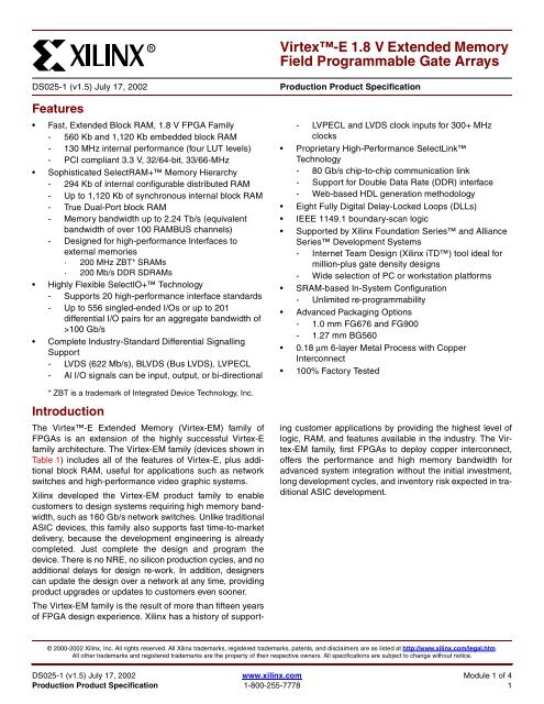
Virtex-E 1.8 V Extended Memory<br />
Field Programmable Gate Arrays<br />
DS025-1 (v1.5) July 17, 2002 0 0 Production Product Specification<br />
- LVPECL and LVDS clock inputs for 300+ MHz<br />
clocks<br />
Proprietary High-Performance SelectLink<br />
Technology<br />
- 80 Gb/s chip-to-chip communication link<br />
- Support for Double Data Rate (DDR) interface<br />
- Web-based HDL generation methodology<br />
Eight Fully Digital Delay-Locked Loops (DLLs)<br />
IEEE 1149.1 boundary-scan logic<br />
Supported by Xilinx Foundation Series and Alliance<br />
Series Development Systems<br />
- Internet Team Design (Xilinx iTD) tool ideal for<br />
million-plus gate density designs<br />
- Wide selection of PC or workstation platforms<br />
SRAM-based In-System Configuration<br />
- Unlimited re-programmability<br />
Advanced Packaging Options<br />
- 1.0 mm FG676 and FG900<br />
- 1.27 mm BG560<br />
0.18 µm 6-layer Metal Process with Copper<br />
Interconnect<br />
100% Factory Tested<br />
ing customer applications by providing the highest level of<br />
logic, RAM, and features available in the industry. The Virtex-EM<br />
family, first FPGAs to deploy copper interconnect,<br />
offers the performance and high memory bandwidth for<br />
advanced system integration without the initial investment,<br />
long development cycles, and inventory risk expected in traditional<br />
ASIC development.<br />
© 2000-2002 Xilinx, Inc. All rights reserved. All Xilinx trademarks, registered trademarks, patents, and disclaimers are as listed at http://www.xilinx.com/legal.htm.<br />
All other trademarks and registered trademarks are the property of their respective owners. All specifications are subject to change without notice.<br />
DS025-1 (v1.5) July 17, 2002 www.xilinx.com Module 1 of 4<br />
Production Product Specification 1-800-255-7778 1
Virtex-E 1.8 V Extended Memory Field Programmable Gate Arrays<br />
Table 1: Virtex-E Extended Memory Field-Programmable Gate Array Family Members<br />
Logic Differential<br />
BlockRAM Distributed<br />
Device Logic Gates CLB Array Cells I/O Pairs User I/O Bits RAM Bits<br />
XCV405E 129,600 40 x 60 10,800 183 404 573,440 153,600<br />
XCV812E 254,016 56 x 84 21,168 201 556 1,146,880 301,056<br />
Virtex-E Compared to Virtex Devices<br />
The Virtex-E family offers up to 43,200 logic cells in devices<br />
up to 30% faster than the Virtex family.<br />
I/O performance is increased to 622 Mb/s using Source<br />
Synchronous data transmission architectures and synchronous<br />
system performance up to 240 MHz using singled-ended<br />
SelectI/O technology. Additional I/O standards<br />
are supported, notably LVPECL, LVDS, and BLVDS, which<br />
use two pins per signal. Almost all signal pins can be used<br />
for these new standards.<br />
Virtex-E devices have up to 640 Kb of faster (250MHz)<br />
block SelectRAM, but the individual RAMs are the same<br />
size and structure as in the Virtex family. They also have<br />
eight DLLs instead of the four in Virtex devices. Each individual<br />
DLL is slightly improved with easier clock mirroring<br />
and 4x frequency multiplication.<br />
VCCINT , the supply voltage for the internal logic and memory,<br />
is 1.8 V, instead of 2.5 V for Virtex devices. Advanced<br />
processing and 0.18 µm design rules have resulted in<br />
smaller dice, faster speed, and lower power consumption.<br />
I/O pins are 3 V tolerant, and can be 5 V tolerant with an<br />
external 100 Ω resistor. PCI 5 V is not supported. With the<br />
addition of appropriate external resistors, any pin can tolerate<br />
any voltage desired.<br />
Banking rules are different. With Virtex devices, all input<br />
buffers are powered by VCCINT. With Virtex-E devices, the<br />
LVTTL, LVCMOS2, and PCI input buffers are powered by<br />
the I/O supply voltage VCCO. The Virtex-E family is not bitstream-compatible with the Virtex<br />
family, but Virtex designs can be compiled into equivalent<br />
Virtex-E devices.<br />
The same device in the same package for the Virtex-E and<br />
Virtex families are pin-compatible with some minor exceptions.<br />
See the data sheet pinout section for details.<br />
General Description<br />
The Virtex-E FPGA family delivers high-performance,<br />
high-capacity programmable logic solutions. Dramatic<br />
increases in silicon efficiency result from optimizing the new<br />
architecture for place-and-route efficiency and exploiting an<br />
aggressive 6-layer metal 0.18 µm CMOS process. These<br />
advances make Virtex-E FPGAs powerful and flexible alter-<br />
natives to mask-programmed gate arrays. The Virtex-E family<br />
includes the nine members in Table 1.<br />
Building on experience gained from Virtex FPGAs, the Virtex-E<br />
family is an evolutionary step forward in programmable<br />
logic design. Combining a wide variety of programmable<br />
system features, a rich hierarchy of fast, flexible interconnect<br />
resources, and advanced process technology, the Virtex-E<br />
family delivers a high-speed and high-capacity<br />
programmable logic solution that enhances design flexibility<br />
while reducing time-to-market.<br />
Virtex-E Architecture<br />
Virtex-E devices feature a flexible, regular architecture that<br />
comprises an array of configurable logic blocks (CLBs) surrounded<br />
by programmable input/output blocks (IOBs), all<br />
interconnected by a rich hierarchy of fast, versatile routing<br />
resources. The abundance of routing resources permits the<br />
Virtex-E family to accommodate even the largest and most<br />
complex designs.<br />
Virtex-E FPGAs are SRAM-based, and are customized by<br />
loading configuration data into internal memory cells. Configuration<br />
data can be read from an external SPROM (master<br />
serial mode), or can be written into the FPGA<br />
(SelectMAP, slave serial, and JTAG modes).<br />
The standard Xilinx Foundation Series and Alliance<br />
Series Development systems deliver complete design<br />
support for Virtex-E, covering every aspect from behavioral<br />
and schematic entry, through simulation, automatic design<br />
translation and implementation, to the creation and downloading<br />
of a configuration bit stream.<br />
Higher Performance<br />
Virtex-E devices provide better performance than previous<br />
generations of FPGAs. Designs can achieve synchronous<br />
system clock rates up to 240 MHz including I/O or 622 Mb/s<br />
using Source Synchronous data transmission architechtures.<br />
Virtex-E I/Os comply fully with 3.3 V PCI specifications,<br />
and interfaces can be implemented that operate at<br />
33 MHz or 66 MHz.<br />
While performance is design-dependent, many designs<br />
operate internally at speeds in excess of 133 MHz and can<br />
achieve over 311 MHz. Table 2, page 3, shows performance<br />
data for representative circuits, using worst-case<br />
timing parameters.<br />
Module 1 of 4 www.xilinx.com DS025-1 (v1.5) July 17, 2002<br />
2 1-800-255-7778 Production Product Specification<br />
R
R<br />
Virtex-E 1.8 V Extended Memory Field Programmable Gate Arrays<br />
Table 2: Performance for Common Circuit Functions<br />
Function Bits Virtex-E -7<br />
Register-to-Register<br />
Adder<br />
Pipelined Multiplier<br />
Address Decoder<br />
Virtex-E Extended Memory Device/Package Combinations and Maximum I/O<br />
Virtex-E Extended Memory Ordering Information<br />
DS025-1 (v1.5) July 17, 2002 www.xilinx.com Module 1 of 4<br />
Production Product Specification 1-800-255-7778 3<br />
16<br />
64<br />
8 x 8<br />
16 x 16<br />
16<br />
64<br />
4.3 ns<br />
6.3 ns<br />
4.4 ns<br />
5.1 ns<br />
3.8 ns<br />
5.5 ns<br />
16:1 Multiplexer 4.6 ns<br />
Parity Tree<br />
Chip-to-Chip<br />
HSTL Class IV<br />
LVTTL,16mA, fast slew<br />
LVDS<br />
LVPECL<br />
9<br />
18<br />
36<br />
3.5 ns<br />
4.3 ns<br />
5.9 ns<br />
Table 3: Virtex-EM Family Maximum User I/O by Device/Package (Excluding Dedicated Clock Pins)<br />
Package XCV405E XCV812E<br />
BG560 404 404<br />
FG676 404<br />
FG900 556<br />
Example: XCV405E-6BG560C<br />
Device Type Temperature Range<br />
C = Commercial (T J = 0˚C to +85˚C)<br />
I = Industrial (T J = −40˚C to +100˚C)<br />
Speed Grade<br />
(-6, -7, -8)<br />
Number of Pins<br />
Package Type<br />
BG = Ball Grid Array<br />
FG = Fine Pitch Ball Grid Array<br />
Figure 1: Virtex Ordering Information<br />
DS025_001_112000
Virtex-E 1.8 V Extended Memory Field Programmable Gate Arrays<br />
Revision History<br />
The following table shows the revision history for this document.<br />
Date Version Revision<br />
03/23/00 1.0 Initial Xilinx release.<br />
08/01/00 1.1 Accumulated edits and fixes. Upgrade to Preliminary. Preview -8 numbers added.<br />
Reformatted to adhere to corporate documentation style guidelines. Minor changes in<br />
BG560 pin-out table.<br />
09/19/00 1.2 In Table 3 (Module 4), FG676 Fine-Pitch BGA — XCV405E, the following pins are no<br />
longer labeled as VREF: B7, G16, G26, W26, AF20, AF8, Y1, H1.<br />
Min values added to Virtex-E Electrical Characteristics tables.<br />
11/20/00 1.3 Updated speed grade -8 numbers in Virtex-E Electrical Characteristics tables<br />
(Module 3).<br />
Updated minimums in Table 11 (Module 2), and added notes to Table 12 (Module 2).<br />
Added to note 2 of Absolute Maximum Ratings (Module 3).<br />
Changed all minimum hold times to –0.4 for Global Clock Set-Up and Hold for LVTTL<br />
Standard, with DLL (Module 3).<br />
Revised maximum TDLLPW in -6 speed grade for DLL Timing Parameters (Module 3).<br />
04/02/01 1.4 In Table 4, FG676 Fine-Pitch BGA — XCV405E, pin B19 is no longer labeled as VREF,<br />
and pin G16 is now labeled as VREF.<br />
Updated values in Virtex-E Switching Characteristics tables.<br />
Converted data sheet to modularized format. See Virtex-E Extended Memory Data<br />
Sheet, below.<br />
07/17/02 1.5 Data sheet designation upgraded from Preliminary to Production.<br />
Virtex-E Extended Memory Data Sheet<br />
The Virtex-E Extended Memory Data Sheet contains the following modules:<br />
DS025-1, Virtex-E 1.8V Extended Memory FPGAs:<br />
Introduction and Ordering Information (Module 1)<br />
DS025-2, Virtex-E 1.8V Extended Memory FPGAs:<br />
Functional Description (Module 2)<br />
DS025-3, Virtex-E 1.8V Extended Memory FPGAs:<br />
DC and Switching Characteristics (Module 3)<br />
DS025-4, Virtex-E 1.8V Extended Memory FPGAs:<br />
Pinout Tables (Module 4)<br />
Module 1 of 4 www.xilinx.com DS025-1 (v1.5) July 17, 2002<br />
4 1-800-255-7778 Production Product Specification<br />
R
Architectural Description<br />
Virtex-E Array<br />
The Virtex-E user-programmable gate array (see Figure 1)<br />
comprises two major configurable elements: configurable<br />
logic blocks (CLBs) and input/output blocks (IOBs).<br />
• CLBs provide the functional elements for constructing<br />
logic.<br />
IOBs provide the interface between the package pins<br />
and the CLBs.<br />
CLBs interconnect through a general routing matrix (GRM).<br />
The GRM comprises an array of routing switches located at<br />
the intersections of horizontal and vertical routing channels.<br />
Each CLB nests into a VersaBlock that also provides local<br />
routing resources to connect the CLB to the GRM.<br />
The VersaRing I/O interface provides additional routing<br />
resources around the periphery of the device. This routing<br />
improves I/O routability and facilitates pin locking.<br />
The Virtex-E architecture also includes the following circuits<br />
that connect to the GRM:<br />
Dedicated block memories of 4096 bits each<br />
Clock DLLs for clock-distribution delay compensation<br />
and clock domain control<br />
3-State buffers (BUFTs) associated with each CLB that<br />
drive dedicated segmentable horizontal routing resources<br />
0<br />
Virtex-E 1.8 V Extended Memory<br />
Field Programmable Gate Arrays<br />
DS025-2 (v2.1) July 17, 2002 0 0 Production Product Specification<br />
IOBs<br />
BRAMs<br />
DLLDLL<br />
CLBs<br />
BRAMs<br />
DLLDLL<br />
Figure 1: Virtex-E Architecture Overview<br />
R<br />
VersaRing<br />
CLBs<br />
CLBs<br />
VersaRing<br />
DLLDLL<br />
BRAMs<br />
CLBs<br />
BRAMs<br />
DLLDLL<br />
IOBs<br />
ds022_001_121099<br />
Values stored in static memory cells control the configurable<br />
logic elements and interconnect resources. These values<br />
load into the memory cells on power-up, and can reload if<br />
necessary to change the function of the device.<br />
Input/Output Block<br />
The Virtex-E IOB, Figure 2, features SelectIO+ inputs and<br />
outputs that support a wide variety of I/O signalling standards<br />
(see Table 1).<br />
Figure 2: Virtex-E Input/Output Block (IOB)<br />
The three IOB storage elements function either as<br />
edge-triggered D-type flip-flops or as level-sensitive latches.<br />
Each IOB has a clock signal (CLK) shared by the three<br />
flip-flops and independent clock enable signals for each<br />
flip-flop.<br />
© 2000-2002 Xilinx, Inc. All rights reserved. All Xilinx trademarks, registered trademarks, patents, and disclaimers are as listed at http://www.xilinx.com/legal.htm.<br />
All other trademarks and registered trademarks are the property of their respective owners. All specifications are subject to change without notice.<br />
DS025-2 (v2.1) July 17, 2002 www.xilinx.com Module 2 of 4<br />
1-800-255-7778 1<br />
T<br />
TCE<br />
O<br />
OCE<br />
I<br />
IQ<br />
SR<br />
CLK<br />
ICE<br />
D Q<br />
CE<br />
SR<br />
D Q<br />
CE<br />
SR<br />
Q D<br />
CE<br />
SR<br />
Programmable<br />
Delay<br />
OBUFT<br />
IBUF<br />
Vref<br />
Weak<br />
Keeper<br />
PAD<br />
ds022_02_091300
Virtex-E 1.8 V Extended Memory Field Programmable Gate Arrays<br />
Table 1: Supported I/O Standards<br />
I/O Output Input Input<br />
Board<br />
Termination<br />
Voltage<br />
Standard VCCO VCCO VREF (VTT )<br />
LVTTL 3.3 3.3 N/A N/A<br />
LVCMOS2 2.5 2.5 N/A N/A<br />
LVCMOS18 1.8 1.8 N/A N/A<br />
SSTL3 I & II 3.3 N/A 1.50 1.50<br />
SSTL2 I & II 2.5 N/A 1.25 1.25<br />
GTL N/A N/A 0.80 1.20<br />
GTL+ N/A N/A 1.0 1.50<br />
HSTL I 1.5 N/A 0.75 0.75<br />
HSTL III & IV 1.5 N/A 0.90 1.50<br />
CTT 3.3 N/A 1.50 1.50<br />
AGP-2X 3.3 N/A 1.32 N/A<br />
PCI33_3 3.3 3.3 N/A N/A<br />
PCI66_3 3.3 3.3 N/A N/A<br />
BLVDS & LVDS 2.5 N/A N/A N/A<br />
LVPECL 3.3 N/A N/A N/A<br />
In addition to the CLK and CE control signals, the three<br />
flip-flops share a Set/Reset (SR). For each flip-flop, this signal<br />
can be independently configured as a synchronous Set,<br />
a synchronous Reset, an asynchronous Preset, or an asynchronous<br />
Clear.<br />
The output buffer and all of the IOB control signals have<br />
independent polarity controls.<br />
All pads are protected against damage from electrostatic<br />
discharge (ESD) and from over-voltage transients. When<br />
PCI 3.3 V compliance is required, a conventional clamp<br />
diode is connected to the output supply voltage, VCCO. Optional pull-up, pull-down and weak-keeper circuits are<br />
attached to each pad. Prior to configuration all outputs not<br />
involved in configuration are forced into their high-impedance<br />
state. The pull-down resistors and the weak-keeper<br />
circuits are inactive, but IOs can optionally be pulled up.<br />
The activation of pull-up resistors prior to configuration is<br />
controlled on a global basis by the configuration mode pins.<br />
If the pull-up resistors are not activated, all the pins are in a<br />
high-impedance state. Consequently, external pull-up or<br />
pull-down resistors must be provided on pins required to be<br />
at a well-defined logic level prior to configuration.<br />
All Virtex-E IOBs support IEEE 1149.1-compatible boundary<br />
scan testing.<br />
Input Path<br />
The Virtex-E IOB input path routes the input signal directly<br />
to internal logic and/ or through an optional input flip-flop.<br />
An optional delay element at the D-input of this flip-flop eliminates<br />
pad-to-pad hold time. The delay is matched to the<br />
internal clock-distribution delay of the FPGA, and when<br />
used, assures that the pad-to-pad hold time is zero.<br />
Each input buffer can be configured to conform to any of the<br />
low-voltage signalling standards supported. In some of<br />
these standards the input buffer utilizes a user-supplied<br />
threshold voltage, VREF . The need to supply VREF imposes<br />
constraints on which standards can be used in close proximity<br />
to each other. See "I/O Banking" on page 2.<br />
There are optional pull-up and pull-down resistors at each<br />
input for use after configuration. Their value is in the range<br />
50 - 100 kΩ.<br />
Output Path<br />
The output path includes a 3-state output buffer that drives<br />
the output signal onto the pad. The output signal can be<br />
routed to the buffer directly from the internal logic or through<br />
an optional IOB output flip-flop.<br />
The 3-state control of the output can also be routed directly<br />
from the internal logic or through a flip-flip that provides synchronous<br />
enable and disable.<br />
Each output driver can be individually programmed for a<br />
wide range of low-voltage signalling standards. Each output<br />
buffer can source up to 24 mA and sink up to 48 mA. Drive<br />
strength and slew rate controls minimize bus transients.<br />
In most signalling standards, the output High voltage<br />
depends on an externally supplied VCCO voltage. The need<br />
to supply VCCO imposes constraints on which standards<br />
can be used in close proximity to each other. See "I/O Banking"<br />
on page 2.<br />
An optional weak-keeper circuit is connected to each output.<br />
When selected, the circuit monitors the voltage on the<br />
pad and weakly drives the pin High or Low to match the<br />
input signal. If the pin is connected to a multiple-source signal,<br />
the weak keeper holds the signal in its last state if all<br />
drivers are disabled. Maintaining a valid logic level in this<br />
way eliminates bus chatter.<br />
Since the weak-keeper circuit uses the IOB input buffer to<br />
monitor the input level, an appropriate VREF voltage must be<br />
provided if the signalling standard requires one. The provision<br />
of this voltage must comply with the I/O banking rules.<br />
I/O Banking<br />
Some of the I/O standards described above require V CCO<br />
and/or V REF voltages. These voltages are externally supplied<br />
and connected to device pins that serve groups of<br />
IOBs, called banks. Consequently, restrictions exist about<br />
which I/O standards can be combined within a given bank.<br />
Module 2 of 4 www.xilinx.com DS025-2 (v2.1) July 17, 2002<br />
2 1-800-255-7778<br />
R
R<br />
Eight I/O banks result from separating each edge of the<br />
FPGA into two banks, as shown in Figure 3. Each bank has<br />
multiple V CCO pins, all of which must be connected to the<br />
same voltage. This voltage is determined by the output<br />
standards in use.<br />
Bank 7<br />
Bank 6<br />
Bank 0<br />
Bank 1<br />
GCLK3 GCLK2<br />
VirtexE<br />
Device<br />
GCLK1 GCLK0<br />
Bank 5 Bank 4<br />
ds022_03_121799<br />
Figure 3: Virtex-E I/O Banks<br />
Within a bank, output standards can be mixed only if they<br />
use the same V CCO . Compatible standards are shown in<br />
Table 2. GTL and GTL+ appear under all voltages because<br />
their open-drain outputs do not depend on V CCO .<br />
Table 2: Compatible Output Standards<br />
VCCO Compatible Standards<br />
3.3 V PCI, LVTTL, SSTL3 I, SSTL3 II, CTT, AGP, GTL,<br />
GTL+, LVPECL<br />
2.5 V SSTL2 I, SSTL2 II, LVCMOS2, GTL, GTL+,<br />
BLVDS, LVDS<br />
1.8 V LVCMOS18, GTL, GTL+<br />
1.5 V HSTL I, HSTL III, HSTL IV, GTL, GTL+<br />
Some input standards require a user-supplied threshold<br />
voltage, V REF . In this case, certain user-I/O pins are automatically<br />
configured as inputs for the V REF voltage. Approximately<br />
one in six of the I/O pins in the bank assume this<br />
role.<br />
Bank 2<br />
Bank 3<br />
Virtex-E 1.8 V Extended Memory Field Programmable Gate Arrays<br />
The VREF pins within a bank are interconnected internally<br />
and consequently only one VREF voltage can be used within<br />
each bank. All VREF pins in the bank, however, must be connected<br />
to the external voltage source for correct operation.<br />
Within a bank, inputs that require VREF can be mixed with<br />
those that do not. However, only one VREF voltage can be<br />
used within a bank.<br />
In Virtex-E, input buffers with LVTTL, LVCMOS2,<br />
LVCMOS18, PCI33_3, PCI66_3 standards are supplied by<br />
VCCO rather than VCCINT . For these standards, only input<br />
and output buffers that have the same VCCO can be mixed<br />
together.<br />
The VCCO and VREF pins for each bank appear in the device<br />
pin-out tables and diagrams. The diagrams also show the<br />
bank affiliation of each I/O.<br />
Within a given package, the number of VREF and VCCO pins<br />
can vary depending on the size of device. In larger devices,<br />
more I/O pins convert to VREF pins. Since these are always<br />
a super set of the VREF pins used for smaller devices, it is<br />
possible to design a PCB that permits migration to a larger<br />
device if necessary. All the VREF pins for the largest device<br />
anticipated must be connected to the VREF voltage, and not<br />
used for I/O.<br />
In smaller devices, some VCCO pins used in larger devices<br />
do not connect within the package. These unconnected pins<br />
can be left unconnected externally, or they can be connected<br />
to the VCCO voltage to permit migration to a larger<br />
device, if necessary.<br />
Configurable Logic Block<br />
The basic building block of the Virtex-E CLB is the logic cell<br />
(LC). An LC includes a 4-input function generator, carry<br />
logic, and a storage element. The output from the function<br />
generator in each LC drives both the CLB output and the D<br />
input of the flip-flop. Each Virtex-E CLB contains four LCs,<br />
organized in two similar slices, as shown in Figure 4.<br />
Figure 5 shows a more detailed view of a single slice.<br />
DS025-2 (v2.1) July 17, 2002 www.xilinx.com Module 2 of 4<br />
1-800-255-7778 3
Virtex-E 1.8 V Extended Memory Field Programmable Gate Arrays<br />
G4<br />
G3<br />
G2<br />
G1<br />
BY<br />
F4<br />
F3<br />
F2<br />
F1<br />
BX<br />
YB<br />
Y<br />
G4<br />
LUT Carry &<br />
Control<br />
SP<br />
D Q<br />
CE<br />
YQ<br />
G3<br />
G2<br />
G1<br />
LUT Carry &<br />
Control<br />
SP<br />
D Q<br />
CE<br />
G4<br />
G3<br />
G2<br />
G1<br />
BY<br />
F5IN<br />
BX<br />
F4<br />
F3<br />
F2<br />
F1<br />
LUT<br />
SR<br />
CLK<br />
CE<br />
Carry &<br />
Control<br />
In addition to the four basic LCs, the Virtex-E CLB contains<br />
logic that combines function generators to provide functions<br />
of five or six inputs. Consequently, when estimating the<br />
number of system gates provided by a given device, each<br />
CLB counts as 4.5 LCs.<br />
COUT COUT<br />
CIN<br />
I3<br />
I2<br />
I1<br />
I0<br />
CK<br />
WE<br />
WSO<br />
A4 WSH<br />
I3<br />
I2<br />
I1<br />
I0<br />
XB<br />
X<br />
XQ<br />
Figure 4: 2-Slice Virtex-E CLB<br />
WE<br />
WE<br />
RC<br />
SP<br />
D Q<br />
CE<br />
LUT<br />
LUT<br />
RC<br />
Look-Up Tables<br />
Virtex-E function generators are implemented as 4-input<br />
look-up tables (LUTs). In addition to operating as a function<br />
generator, each LUT can provide a 16 x 1-bit synchronous<br />
RAM. Furthermore, the two LUTs within a slice can be com-<br />
Module 2 of 4 www.xilinx.com DS025-2 (v2.1) July 17, 2002<br />
4 1-800-255-7778<br />
BY<br />
F4<br />
F3<br />
F2<br />
F1<br />
BX<br />
LUT<br />
Carry &<br />
Control<br />
Slice 1 Slice 0<br />
DI<br />
BY DG<br />
BX DI<br />
O<br />
DI<br />
O<br />
0<br />
1<br />
0<br />
1<br />
COUT<br />
CY<br />
CY<br />
Figure 5: Detailed View of Virtex-E Slice<br />
CIN<br />
F5<br />
F6<br />
CIN<br />
D<br />
CE Q<br />
INIT<br />
REV<br />
INIT<br />
D Q<br />
CE<br />
REV<br />
RC<br />
SP<br />
D Q<br />
CE<br />
RC<br />
YB<br />
Y<br />
YQ<br />
XB<br />
X<br />
XQ<br />
ds022_04_121799<br />
YB<br />
Y<br />
YQ<br />
XB<br />
F5<br />
X<br />
XQ<br />
ds022_05_092000<br />
R
R<br />
bined to create a 16 x 2-bit or 32 x 1-bit synchronous RAM,<br />
or a 16 x 1-bit dual-port synchronous RAM.<br />
The Virtex-E LUT can also provide a 16-bit shift register that<br />
is ideal for capturing high-speed or burst-mode data. This<br />
mode can also be used to store data in applications such as<br />
Digital Signal Processing.<br />
Storage Elements<br />
The storage elements in the Virtex-E slice can be configured<br />
either as edge-triggered D-type flip-flops or as<br />
level-sensitive latches. The D inputs can be driven either by<br />
the function generators within the slice or directly from slice<br />
inputs, bypassing the function generators.<br />
In addition to Clock and Clock Enable signals, each Slice<br />
has synchronous set and reset signals (SR and BY). SR<br />
forces a storage element into the initialization state specified<br />
for it in the configuration. BY forces it into the opposite<br />
state. Alternatively, these signals can be configured to operate<br />
asynchronously. All of the control signals are independently<br />
invertible, and are shared by the two flip-flops within<br />
the slice.<br />
Additional Logic<br />
The F5 multiplexer in each slice combines the function generator<br />
outputs. This combination provides either a function<br />
generator that can implement any 5-input function, a 4:1<br />
multiplexer, or selected functions of up to nine inputs.<br />
Similarly, the F6 multiplexer combines the outputs of all four<br />
function generators in the CLB by selecting one of the<br />
F5-multiplexer outputs. This permits the implementation of<br />
any 6-input function, an 8:1 multiplexer, or selected functions<br />
of up to 19 inputs.<br />
Each CLB has four direct feedthrough paths, two per slice.<br />
These paths provide extra data input lines or additional local<br />
routing that does not consume logic resources.<br />
Table 3: CLB/Block RAM Column Locations<br />
Table 4 shows the amount of block SelectRAM memory that<br />
is available in each Virtex-E device.<br />
Virtex-E 1.8 V Extended Memory Field Programmable Gate Arrays<br />
Arithmetic Logic<br />
Dedicated carry logic provides fast arithmetic carry capability<br />
for high-speed arithmetic functions. The Virtex-E CLB<br />
supports two separate carry chains, one per Slice. The<br />
height of the carry chains is two bits per CLB.<br />
The arithmetic logic includes an XOR gate that allows a<br />
2-bit full adder to be implemented within a slice. In addition,<br />
a dedicated AND gate improves the efficiency of multiplier<br />
implementation.<br />
The dedicated carry path can also be used to cascade function<br />
generators for implementing wide logic functions.<br />
BUFTs<br />
Each Virtex-E CLB contains two 3-state drivers (BUFTs)<br />
that can drive on-chip busses. See "Dedicated Routing" on<br />
page 7. Each Virtex-E BUFT has an independent 3-state<br />
control pin and an independent input pin.<br />
Block SelectRAM<br />
Virtex-E FPGAs incorporate large block SelectRAM memories.<br />
These complement the Distributed SelectRAM memories<br />
that provide shallow RAM structures implemented in<br />
CLBs.<br />
Block SelectRAM memory blocks are organized in columns,<br />
starting at the left (column 0) and right outside edges and<br />
inserted every four CLB columns (see notes for smaller<br />
devices). Each memory block is four CLBs high, and each<br />
memory column extends the full height of the chip, immediately<br />
adjacent (to the right, except for column 0) of the CLB<br />
column locations indicated in Table 3.<br />
Virtex-E Device 0 4 8 12 16 20 24 28 32 36 40 44 48 52 56 60 64 68 72 76 80 84<br />
XCV405E √ √ √ √ √ √ √ √ √ √ √ √ √ √<br />
XCV812E √ √ √ √ √ √ √ √ √ √ √ √ √ √ √ √ √ √ √ √<br />
Table 4: Virtex-E Block SelectRAM Amounts<br />
Virtex-E Device # of Blocks Block SelectRAM Bits<br />
XCV405E 140 573,440<br />
XCV812E 280 1,146,880<br />
Each block SelectRAM cell, as illustrated in Figure 6, is a<br />
fully synchronous dual-ported (True Dual Port) 4096-bit<br />
RAM with independent control signals for each port. The<br />
data widths of the two ports can be configured independently,<br />
providing built-in bus-width conversion.<br />
DS025-2 (v2.1) July 17, 2002 www.xilinx.com Module 2 of 4<br />
1-800-255-7778 5
Virtex-E 1.8 V Extended Memory Field Programmable Gate Arrays<br />
Table 5 shows the depth and width aspect ratios for the<br />
block SelectRAM. The Virtex-E block SelectRAM also<br />
includes dedicated routing to provide an efficient interface<br />
with both CLBs and other block SelectRAM modules.<br />
Programmable Routing Matrix<br />
It is the longest delay path that limits the speed of any<br />
worst-case design. Consequently, the Virtex-E routing<br />
architecture and its place-and-route software were defined<br />
in a joint optimization process. This joint optimization minimizes<br />
long-path delays, and consequently, yields the best<br />
system performance.<br />
The joint optimization also reduces design compilation<br />
times because the architecture is software-friendly. Design<br />
cycles are correspondingly reduced due to shorter design<br />
iteration times.<br />
Local Routing<br />
WEA<br />
ENA<br />
RSTA<br />
CLKA<br />
ADDRA[#:0]<br />
DIA[#:0]<br />
WEB<br />
ENB<br />
RSTB<br />
CLKB<br />
ADDRB[#:0]<br />
DIB[#:0]<br />
RAMB4_S#_S#<br />
DOA[#:0]<br />
DOB[#:0]<br />
ds022_06_121699<br />
Figure 6: Dual-Port Block SelectRAM<br />
Table 5: Block SelectRAM Port Aspect Ratios<br />
Width Depth ADDR Bus Data Bus<br />
1 4096 ADDR DATA<br />
2 2048 ADDR DATA<br />
4 1024 ADDR DATA<br />
8 512 ADDR DATA<br />
16 256 ADDR DATA<br />
The VersaBlock, shown in Figure 7, provides local routing<br />
resources with the following types of connections:<br />
Interconnections among the LUTs, flip-flops, and GRM<br />
Internal CLB feedback paths that provide high-speed<br />
connections to LUTs within the same CLB, chaining<br />
them together with minimal routing delay<br />
Direct paths that provide high-speed connections<br />
between horizontally adjacent CLBs, eliminating the<br />
delay of the GRM<br />
Module 2 of 4 www.xilinx.com DS025-2 (v2.1) July 17, 2002<br />
6 1-800-255-7778<br />
.<br />
To<br />
Adjacent<br />
GRM<br />
General Purpose Routing<br />
Most Virtex-E signals are routed on the general purpose<br />
routing, and consequently, the majority of interconnect<br />
resources are associated with this level of the routing hierarchy.<br />
The general routing resources are located in horizontal<br />
and vertical routing channels associated with the CLB<br />
rows and columns. The general-purpose routing resources<br />
are listed below.<br />
Adjacent to each CLB is a General Routing Matrix<br />
(GRM). The GRM is the switch matrix through which<br />
horizontal and vertical routing resources connect, and<br />
is also the means by which the CLB gains access to<br />
the general purpose routing.<br />
24 single-length lines route GRM signals to adjacent<br />
GRMs in each of the four directions.<br />
72 buffered Hex lines route GRM signals to another<br />
GRMs six-blocks away in each one of the four<br />
directions. Organized in a staggered pattern, Hex lines<br />
are driven only at their endpoints. Hex-line signals can<br />
be accessed either at the endpoints or at the midpoint<br />
(three blocks from the source). One third of the Hex<br />
lines are bidirectional, while the remaining ones are<br />
uni-directional.<br />
12 Longlines are buffered, bidirectional wires that<br />
distribute signals across the device quickly and<br />
efficiently. Vertical Longlines span the full height of the<br />
device, and horizontal ones span the full width of the<br />
device.<br />
I/O Routing<br />
To Adjacent<br />
GRM<br />
GRM<br />
To Adjacent<br />
GRM<br />
Direct Connection<br />
To Adjacent<br />
CLB<br />
To Adjacent<br />
GRM<br />
Figure 7: Virtex-E Local Routing<br />
XCVE_ds_007<br />
Virtex-E devices have additional routing resources around<br />
their periphery that form an interface between the CLB array<br />
and the IOBs. This additional routing, called the VersaRing,<br />
facilitates pin-swapping and pin-locking, such that logic<br />
redesigns can adapt to existing PCB layouts. Time-to-market<br />
is reduced, since PCBs and other system components<br />
can be manufactured while the logic design is still in<br />
progress.<br />
CLB<br />
Direct<br />
Connection<br />
To Adjacent<br />
CLB<br />
R
R<br />
Dedicated Routing<br />
Some signal classes require dedicated routing resources to<br />
maximize performance. In the Virtex-E architecture, dedicated<br />
routing resources are provided for two signal classes.<br />
Horizontal routing resources are provided for on-chip<br />
3-state busses. Four partitionable bus lines are<br />
provided per CLB row, permitting multiple busses<br />
within a row, as shown in Figure 8.<br />
Clock Routing<br />
Clock Routing resources distribute clocks and other signals<br />
with very high fanout throughout the device. Virtex-E<br />
devices include two tiers of clock routing resources referred<br />
to as global and local clock routing resources.<br />
The global routing resources are four dedicated global<br />
nets with dedicated input pins that are designed to<br />
distribute high-fanout clock signals with minimal skew.<br />
Each global clock net can drive all CLB, IOB, and block<br />
RAM clock pins. The global nets can be driven only by<br />
global buffers. There are four global buffers, one for<br />
each global net.<br />
Global Clock Distribution<br />
Virtex-E provides high-speed, low-skew clock distribution<br />
through the global routing resources described above. A<br />
typical clock distribution net is shown in Figure 9.<br />
Global Clock Rows<br />
Virtex-E 1.8 V Extended Memory Field Programmable Gate Arrays<br />
Two dedicated nets per CLB propagate carry signals<br />
vertically to the adjacent CLB. Global Clock Distribution<br />
Network.<br />
DLL Location<br />
CLB CLB CLB CLB<br />
GCLKPAD3<br />
GCLKBUF3<br />
GCLKBUF1<br />
GCLKPAD1<br />
Figure 8: BUFT Connections to Dedicated Horizontal Bus LInes<br />
GCLKPAD2<br />
GCLKBUF2<br />
Global Clock Column<br />
GCLKBUF0<br />
GCLKPAD0<br />
XCVE_009<br />
Figure 9: Global Clock Distribution Network<br />
Global Clock Spine<br />
The local clock routing resources consist of 24<br />
backbone lines, 12 across the top of the chip and 12<br />
across bottom. From these lines, up to 12 unique<br />
signals per column can be distributed via the 12<br />
longlines in the column. These local resources are<br />
more flexible than the global resources since they are<br />
not restricted to routing only to clock pins.<br />
Four global buffers are provided, two at the top center of the<br />
device and two at the bottom center. These drive the four<br />
global nets that in turn drive any clock pin.<br />
Four dedicated clock pads are provided, one adjacent to<br />
each of the global buffers. The input to the global buffer is<br />
selected either from these pads or from signals in the general<br />
purpose routing.<br />
Digital Delay-Locked Loops<br />
buft_c.eps<br />
Tri-State<br />
Lines<br />
There are eight DLLs (Delay-Locked Loops) per device,<br />
with four located at the top and four at the bottom,<br />
Figure 10. The DLLs can be used to eliminate skew<br />
between the clock input pad and the internal clock input pins<br />
throughout the device. Each DLL can drive two global clock<br />
networks.The DLL monitors the input clock and the distributed<br />
clock, and automatically adjusts a clock delay element.<br />
Additional delay is introduced such that clock edges arrive<br />
at internal flip-flops synchronized with clock edges arriving<br />
at the input.<br />
In addition to eliminating clock-distribution delay, the DLL<br />
provides advanced control of multiple clock domains. The<br />
DS025-2 (v2.1) July 17, 2002 www.xilinx.com Module 2 of 4<br />
1-800-255-7778 7
Virtex-E 1.8 V Extended Memory Field Programmable Gate Arrays<br />
DLL provides four quadrature phases of the source clock,<br />
and can double the clock or divide the clock by 1.5, 2, 2.5, 3,<br />
4, 5, 8, or 16.<br />
The DLL also operates as a clock mirror. By driving the output<br />
from a DLL off-chip and then back on again, the DLL can be<br />
used to de-skew a board level clock among multiple devices.<br />
In order to guarantee that the system clock is operating correctly<br />
prior to the FPGA starting up after configuration, the<br />
DLL can delay the completion of the configuration process<br />
until after it has achieved lock.<br />
For more information about DLL functionality, see the<br />
Design Consideration section of the data sheet.<br />
Boundary Scan<br />
Virtex-E devices support all the mandatory boundary-scan<br />
instructions specified in the IEEE standard 1149.1. A Test<br />
Access Port (TAP) and registers are provided that implement<br />
the EXTEST, INTEST, SAMPLE/PRELOAD, BYPASS,<br />
IDCODE, USERCODE, and HIGHZ instructions. The TAP<br />
also supports two internal scan chains and configuration/readback<br />
of the device.<br />
The JTAG input pins (TDI, TMS, TCK) do not have a VCCO requirement, and operate with either 2.5 V or 3.3 V input<br />
signalling levels. The output pin (TDO) is sourced from the<br />
VCCO in bank 2, and for proper operation of LVTTL 3.3 V<br />
levels, the bank should be supplied with 3.3 V.<br />
Boundary-scan operation is independent of individual IOB<br />
configurations, and unaffected by package type. All IOBs,<br />
including un-bonded ones, are treated as independent<br />
3-state bidirectional pins in a single scan chain. Retention of<br />
the bidirectional test capability after configuration facilitates<br />
the testing of external interconnections.<br />
Table 6 lists the boundary-scan instructions supported in<br />
Virtex-E FPGAs. Internal signals can be captured during<br />
EXTEST by connecting them to un-bonded or unused IOBs.<br />
They can also be connected to the unused outputs of IOBs<br />
defined as unidirectional input pins.<br />
Before the device is configured, all instructions except<br />
USER1 and USER2 are available. After configuration, all<br />
instructions are available. During configuration, it is recommended<br />
that those operations using the boundary-scan<br />
register (SAMPLE/PRELOAD, INTEST, EXTEST) not be<br />
performed.<br />
In addition to the test instructions outlined above, the<br />
boundary-scan circuitry can be used to configure the<br />
FPGA, and also to read back the configuration data.<br />
Module 2 of 4 www.xilinx.com DS025-2 (v2.1) July 17, 2002<br />
8 1-800-255-7778<br />
Secondary DLLs<br />
DLLDLL<br />
DLLDLL<br />
Primary DLLs<br />
DLLDLL<br />
DLLDLL<br />
Secondary DLLs<br />
Figure 10: DLL Locations<br />
XCVE_0010<br />
R
R<br />
Virtex-E 1.8 V Extended Memory Field Programmable Gate Arrays<br />
Figure 11 is a diagram of the Virtex-E Series boundary scan logic. It includes three bits of Data Register per IOB, the IEEE<br />
1149.1 Test Access Port controller, and the Instruction Register with decodes.<br />
TDI<br />
IOB<br />
IOB<br />
IOB<br />
IOB<br />
IOB<br />
IOB<br />
IOB<br />
IOB IOB<br />
IOB IOB IOB<br />
BYPASS<br />
REGISTER<br />
INSTRUCTION REGISTER<br />
IOB<br />
IOB<br />
IOB<br />
IOB<br />
IOB<br />
IOB<br />
IOB<br />
M<br />
U<br />
X<br />
TDO<br />
IOB.T<br />
IOB.I<br />
IOB.Q<br />
IOB.T<br />
IOB.I<br />
SHIFT/<br />
CAPTURE<br />
Figure 11: Virtex-E Family Boundary Scan Logic<br />
DS025-2 (v2.1) July 17, 2002 www.xilinx.com Module 2 of 4<br />
1-800-255-7778 9<br />
DATA IN<br />
1<br />
0<br />
1<br />
0<br />
1<br />
0<br />
1<br />
0<br />
1<br />
0<br />
D Q<br />
D Q<br />
D Q<br />
D Q<br />
D Q<br />
sd<br />
D Q<br />
LE<br />
sd<br />
D Q<br />
LE<br />
sd<br />
D Q<br />
LE<br />
sd<br />
D Q<br />
LE<br />
sd<br />
D Q<br />
DATAOUT UPDATE EXTEST<br />
CLOCK DATA<br />
REGISTER<br />
LE<br />
0<br />
1<br />
1<br />
0<br />
1<br />
0<br />
0<br />
1<br />
1<br />
0<br />
X9016
Virtex-E 1.8 V Extended Memory Field Programmable Gate Arrays<br />
Table 6: Boundary Scan Instructions<br />
Boundary-Scan<br />
Command<br />
Instruction Set<br />
The Virtex-E Series boundary scan instruction set also<br />
includes instructions to configure the device and read back<br />
configuration data (CFG_IN, CFG_OUT, and JSTART). The<br />
complete instruction set is coded as shown in Table 6.<br />
Data Registers<br />
Binary<br />
Code (4:0) Description<br />
EXTEST 00000 Enable boundary-scan<br />
EXTEST operation.<br />
SAMPLE/<br />
PRELOAD<br />
00001 Enable boundary-scan<br />
SAMPLE/PRELOAD<br />
operation.<br />
USER1 00010 Access user-defined<br />
register 1.<br />
USER2 00011 Access user-defined<br />
register 2.<br />
CFG_OUT 00100 Access the<br />
configuration bus for<br />
read operations.<br />
CFG_IN 00101 Access the<br />
configuration bus for<br />
write operations.<br />
INTEST 00111 Enable boundary-scan<br />
INTEST operation.<br />
USERCODE 01000 Enable shifting out<br />
USER code.<br />
IDCODE 01001 Enable shifting out of ID<br />
Code.<br />
HIGHZ 01010 3-state output pins while<br />
enabling the Bypass<br />
Register.<br />
JSTART 01100 Clock the start-up<br />
sequence when<br />
StartupClk is TCK.<br />
BYPASS 11111 Enable BYPASS.<br />
RESERVED All other<br />
codes<br />
Xilinx reserved<br />
instructions.<br />
The primary data register is the boundary scan register. For<br />
each IOB pin in the FPGA, bonded or not, it includes three<br />
bits for In, Out, and 3-State Control. Non-IOB pins have<br />
appropriate partial bit population if input-only or output-only.<br />
Each EXTEST CAPTURED-OR state captures all In, Out,<br />
and 3-state pins.<br />
The other standard data register is the single flip-flop<br />
BYPASS register. It synchronizes data being passed<br />
through the FPGA to the next downstream boundary scan<br />
device.<br />
The FPGA supports up to two additional internal scan<br />
chains that can be specified using the BSCAN macro. The<br />
macro provides two user pins (SEL1 and SEL2) which are<br />
decodes of the USER1 and USER2 instructions respectively.<br />
For these instructions, two corresponding pins (T<br />
DO1 and TDO2) allow user scan data to be shifted out of<br />
TDO.<br />
Likewise, there are individual clock pins (DRCK1 and<br />
DRCK2) for each user register. There is a common input pin<br />
(TDI) and shared output pins that represent the state of the<br />
TAP controller (RESET, SHIFT, and UPDATE).<br />
Bit Sequence<br />
The order within each IOB is: In, Out, 3-State. The<br />
input-only pins contribute only the In bit to the boundary<br />
scan I/O data register, while the output-only pins contributes<br />
all three bits.<br />
From a cavity-up view of the chip (as shown in EPIC), starting<br />
in the upper right chip corner, the boundary scan<br />
data-register bits are ordered as shown in Figure 12.<br />
BSDL (Boundary Scan Description Language) files for Virtex-E<br />
Series devices are available on the Xilinx web site in<br />
the File Download area.<br />
Bit 0 ( TDO end)<br />
Bit 1<br />
Bit 2<br />
Figure 12: Boundary Scan Bit Sequence<br />
Module 2 of 4 www.xilinx.com DS025-2 (v2.1) July 17, 2002<br />
10 1-800-255-7778<br />
(TDI end)<br />
Right half of top-edge IOBs (Right to Left)<br />
GCLK2<br />
GCLK3<br />
Left half of top-edge IOBs (Right to Left)<br />
Left-edge IOBs (Top to Bottom)<br />
M1<br />
M0<br />
M2<br />
Left half of bottom-edge IOBs (Left to Right)<br />
GCLK1<br />
GCLK0<br />
Right half of bottom-edge IOBs (Left to Right)<br />
DONE<br />
PROG<br />
Right-edge IOBs (Bottom to Top)<br />
CCLK<br />
990602001<br />
R
R<br />
Identification Registers<br />
The IDCODE register is supported. By using the IDCODE,<br />
the device connected to the JTAG port can be determined.<br />
The IDCODE register has the following binary format:<br />
vvvv:ffff:fffa:aaaa:aaaa:cccc:cccc:ccc1<br />
where<br />
v = the die version number<br />
f = the family code (05 for Virtex-E family)<br />
a = the number of CLB rows (ranges from 16 for<br />
XCV50E to 104 for XCV3200E)<br />
c = the company code (49h for Xilinx)<br />
The USERCODE register is supported. By using the USER-<br />
CODE, a user-programmable identification code can be<br />
loaded and shifted out for examination. The identification<br />
code (see Table 7) is embedded in the bitstream during bitstream<br />
generation and is valid only after configuration.<br />
Development System<br />
Virtex-E FPGAs are supported by the Xilinx Foundation and<br />
Alliance Series CAE tools. The basic methodology for Virtex-E<br />
design consists of three interrelated steps: design<br />
entry, implementation, and verification. Industry-standard<br />
tools are used for design entry and simulation (for example,<br />
Synopsys FPGA Express), while Xilinx provides proprietary<br />
architecture-specific tools for implementation.<br />
The Xilinx development system is integrated under the Xilinx<br />
Design Manager (XDM) software, providing designers<br />
with a common user interface regardless of their choice of<br />
entry and verification tools. The XDM software simplifies the<br />
selection of implementation options with pull-down menus<br />
and on-line help.<br />
Application programs ranging from schematic capture to<br />
Placement and Routing (PAR) can be accessed through the<br />
XDM software. The program command sequence is generated<br />
prior to execution, and stored for documentation.<br />
Several advanced software features facilitate Virtex-E design.<br />
RPMs, for example, are schematic-based macros with relative<br />
location constraints to guide their placement. They help<br />
ensure optimal implementation of common functions.<br />
For HDL design entry, the Xilinx FPGA Foundation development<br />
system provides interfaces to the following synthesis<br />
design environments.<br />
Synopsys (FPGA Compiler, FPGA Express)<br />
Exemplar (Spectrum)<br />
Synplicity (Synplify)<br />
For schematic design entry, the Xilinx FPGA Foundation<br />
and Alliance development system provides interfaces to the<br />
following schematic-capture design environments.<br />
Mentor Graphics V8 (Design Architect, QuickSim II)<br />
Viewlogic Systems (Viewdraw)<br />
Third-party vendors support many other environments.<br />
Virtex-E 1.8 V Extended Memory Field Programmable Gate Arrays<br />
Table 7: IDCODEs Assigned to Virtex-E FPGAs<br />
FPGA IDCODE<br />
XCV405EM v0C28093h<br />
XCV812EM v0C38093h<br />
Note:<br />
Attempting to load an incorrect bitstream causes<br />
configuration to fail and can damage the device.<br />
Including Boundary Scan in a Design<br />
Since the boundary scan pins are dedicated, no special element<br />
needs to be added to the design unless an internal<br />
data register (USER1 or USER2) is desired.<br />
If an internal data register is used, insert the boundary scan<br />
symbol and connect the necessary pins as appropriate.<br />
A standard interface-file specification, Electronic Design<br />
Interchange Format (EDIF), simplifies file transfers into and<br />
out of the development system.<br />
Virtex-E FPGAs are supported by a unified library of standard<br />
functions. This library contains over 400 primitives and<br />
macros, ranging from 2-input AND gates to 16-bit accumulators,<br />
and includes arithmetic functions, comparators,<br />
counters, data registers, decoders, encoders, I/O functions,<br />
latches, Boolean functions, multiplexers, shift registers, and<br />
barrel shifters.<br />
The “soft macro” portion of the library contains detailed<br />
descriptions of common logic functions, but does not contain<br />
any partitioning or placement information. The performance<br />
of these macros depends, therefore, on the<br />
partitioning and placement obtained during implementation.<br />
RPMs, on the other hand, do contain predetermined partitioning<br />
and placement information that permits optimal<br />
implementation of these functions. Users can create their<br />
own library of soft macros or RPMs based on the macros<br />
and primitives in the standard library.<br />
The design environment supports hierarchical design entry,<br />
with high-level schematics that comprise major functional<br />
blocks, while lower-level schematics define the logic in<br />
these blocks. These hierarchical design elements are automatically<br />
combined by the implementation tools. Different<br />
design entry tools can be combined within a hierarchical<br />
design, thus allowing the most convenient entry method to<br />
be used for each portion of the design.<br />
Design Implementation<br />
The place-and-route tools (PAR) automatically provide the<br />
implementation flow described in this section. The partitioner<br />
takes the EDIF net list for the design and maps the<br />
logic into the architectural resources of the FPGA (CLBs<br />
and IOBs, for example). The placer then determines the<br />
best locations for these blocks based on their interconnec-<br />
DS025-2 (v2.1) July 17, 2002 www.xilinx.com Module 2 of 4<br />
1-800-255-7778 11
Virtex-E 1.8 V Extended Memory Field Programmable Gate Arrays<br />
tions and the desired performance. Finally, the router interconnects<br />
the blocks.<br />
The PAR algorithms support fully automatic implementation<br />
of most designs. For demanding applications, however, the<br />
user can exercise various degrees of control over the process.<br />
User partitioning, placement, and routing information<br />
is optionally specified during the design-entry process. The<br />
implementation of highly structured designs can benefit<br />
greatly from basic floor planning.<br />
The implementation software incorporates Timing Wizard ®<br />
timing-driven placement and routing. Designers specify timing<br />
requirements along entire paths during design entry.<br />
The timing path analysis routines in PAR then recognize<br />
these user-specified requirements and accommodate them.<br />
Timing requirements are entered on a schematic in a form<br />
directly relating to the system requirements, such as the targeted<br />
clock frequency, or the maximum allowable delay<br />
between two registers. In this way, the overall performance<br />
of the system along entire signal paths is automatically tailored<br />
to user-generated specifications. Specific timing information<br />
for individual nets is unnecessary.<br />
Configuration<br />
Virtex-E devices are configured by loading configuration<br />
data into the internal configuration memory. Note that<br />
attempting to load an incorrect bitstream causes configuration<br />
to fail and can damage the device.<br />
Some of the pins used for configuration are dedicated pins,<br />
while others can be re-used as general purpose inputs and<br />
outputs once configuration is complete.<br />
The following are dedicated pins:<br />
Mode pins (M2, M1, M0)<br />
Configuration clock pin (CCLK)<br />
PROGRAM pin<br />
DONE pin<br />
Boundary-scan pins (TDI, TDO, TMS, TCK)<br />
Depending on the configuration mode chosen, CCLK can<br />
be an output generated by the FPGA, or it can be generated<br />
externally and provided to the FPGA as an input. For correct<br />
operation, these pins require a V CCO of 3.3 V to permit<br />
LVTTL operation. All of the pins affected are in banks 2 or 3.<br />
Design Verification<br />
In addition to conventional software simulation, FPGA users<br />
can use in-circuit debugging techniques. Because Xilinx<br />
devices are infinitely reprogrammable, designs can be verified<br />
in real time without the need for extensive sets of software<br />
simulation vectors.<br />
The development system supports both software simulation<br />
and in-circuit debugging techniques. For simulation, the<br />
system extracts the post-layout timing information from the<br />
design database, and back-annotates this information into<br />
the net list for use by the simulator. Alternatively, the user<br />
can verify timing-critical portions of the design using the<br />
TRCE ® static timing analyzer.<br />
For in-circuit debugging, an optional download and readback<br />
cable is available. This cable connects the FPGA in the<br />
target system to a PC or workstation. After downloading the<br />
design into the FPGA, the designer can single-step the<br />
logic, readback the contents of the flip-flops, and so observe<br />
the internal logic state. Simple modifications can be downloaded<br />
into the system in a matter of minutes.<br />
Configuration Modes<br />
Virtex-E supports the following four configuration modes.<br />
Slave-serial mode<br />
Master-serial mode<br />
SelectMAP mode<br />
Boundary-scan mode (JTAG)<br />
The Configuration mode pins (M2, M1, M0) select among<br />
these configuration modes with the option in each case of<br />
having the IOB pins either pulled up or left floating prior to<br />
configuration. The selection codes are listed in Table 8.<br />
Configuration through the boundary-scan port is always<br />
available, independent of the mode selection. Selecting the<br />
boundary-scan mode simply turns off the other modes. The<br />
three mode pins have internal pull-up resistors, and default<br />
to a logic High if left unconnected.<br />
Table 8: Configuration Codes<br />
Configuration Mode M2 M1 M0 CCLK Direction Data Width Serial Dout Configuration Pull-ups<br />
Master-serial mode 0 0 0 Out 1 Yes No<br />
Boundary-scan mode 1 0 1 N/A 1 No No<br />
SelectMAP mode 1 1 0 In 8 No No<br />
Slave-serial mode 1 1 1 In 1 Yes No<br />
Master-serial mode 1 0 0 Out 1 Yes Yes<br />
Boundary-scan mode 0 0 1 N/A 1 No Yes<br />
SelectMAP mode 0 1 0 In 8 No Yes<br />
Slave-serial mode 0 1 1 In 1 Yes Yes<br />
Module 2 of 4 www.xilinx.com DS025-2 (v2.1) July 17, 2002<br />
12 1-800-255-7778<br />
R
R<br />
Table 9 lists the total number of bits required to configure<br />
each device.<br />
Table 9: Virtex-E Bitstream Lengths<br />
Device # of Configuration Bits<br />
XCV405E 3,430,400<br />
XCV812E 6,519,648<br />
Slave-Serial Mode<br />
In slave-serial mode, the FPGA receives configuration data<br />
in bit-serial form from a serial PROM or other source of<br />
serial configuration data. The serial bitstream must be set<br />
up at the DIN input pin a short time before each rising edge<br />
of an externally generated CCLK.<br />
For more information on serial PROMs, see the PROM data<br />
sheet at http://www.xilinx.com/partinfo/ds026.<strong>pdf</strong>.<br />
Multiple FPGAs can be daisy-chained for configuration from<br />
a single source. After a particular FPGA has been config-<br />
Table 10: Master/Slave Serial Mode Programming Switching<br />
CCLK<br />
Description<br />
Virtex-E 1.8 V Extended Memory Field Programmable Gate Arrays<br />
ured, the data for the next device is routed to the DOUT pin.<br />
Data on the DOUT pin changes on the rising edge of CCLK.<br />
The change of DOUT on the rising edge of CCLK differs<br />
from previous families but does not cause a problem for<br />
mixed configuration chains. This change was made to<br />
improve serial configuration rates for Virtex and Virtex-E<br />
only chains.<br />
Figure 13 shows a full master/slave system. A Virtex-E<br />
device in slave-serial mode should be connected as shown<br />
in the right-most device.<br />
Slave-serial mode is selected by applying or <br />
to the mode pins (M2, M1, M0). A weak pull-up on the mode<br />
pins makes slave-serial the default mode if the pins are left<br />
unconnected. Figure 14 shows slave-serial configuration<br />
timing.<br />
Table 10 provides more detail about the characteristics<br />
shown in Figure 14. Configuration must be delayed until the<br />
INIT pins of all daisy-chained FPGAs are High.<br />
Figure<br />
References Symbol Values Units<br />
DIN setup/hold, slave mode 1/2 T DCC/T CCD 5.0/0.0 ns, min<br />
DIN setup/hold, master mode 1/2 T DSCK/T CKDS 5.0/0.0 ns, min<br />
DOUT 3 T CCO 12.0 ns, max<br />
High time 4 T CCH 5.0 ns, min<br />
Low time 5 T CCL 5.0 ns, min<br />
Maximum Frequency F CC 66 MHz, max<br />
Frequency Tolerance, master mode with respect to nominal +45% –30%<br />
PROGRAM<br />
M0 M1<br />
M2<br />
VIRTEX-E<br />
MASTER<br />
SERIAL<br />
DOUT<br />
3.3V<br />
4.7 K<br />
XC1701L<br />
VIRTEX-E,<br />
XC4000XL,<br />
SLAVE<br />
CCLK CLK<br />
DIN<br />
DATA<br />
PROGRAM CE CEO<br />
PROGRAM<br />
DONE INIT<br />
RESET/OE<br />
DONE<br />
Figure 13: Master/Slave Serial Mode Circuit Diagram<br />
DS025-2 (v2.1) July 17, 2002 www.xilinx.com Module 2 of 4<br />
1-800-255-7778 13<br />
N/C<br />
(Low Reset Option Used)<br />
N/C<br />
M0 M1<br />
M2<br />
DIN DOUT<br />
CCLK<br />
INIT<br />
XCVE_ds_013
Virtex-E 1.8 V Extended Memory Field Programmable Gate Arrays<br />
Master-Serial Mode<br />
In master-serial mode, the CCLK output of the FPGA drives<br />
a Xilinx Serial PROM that feeds bit-serial data to the DIN<br />
input. The FPGA accepts this data on each rising CCLK<br />
edge. After the FPGA has been loaded, the data for the next<br />
device in a daisy-chain is presented on the DOUT pin after<br />
the rising CCLK edge.<br />
The interface is identical to slave-serial except that an internal<br />
oscillator is used to generate the configuration clock<br />
(CCLK). A wide range of frequencies can be selected for<br />
CCLK which always starts at a slow default frequency. Configuration<br />
bits then switch CCLK to a higher frequency for<br />
the remainder of the configuration. Switching to a lower frequency<br />
is prohibited.<br />
The CCLK frequency is set using the ConfigRate option in<br />
the bitstream generation software. The maximum CCLK frequency<br />
that can be selected is 60 MHz. When selecting a<br />
CCLK frequency, ensure that the serial PROM and any<br />
daisy-chained FPGAs are fast enough to support the clock<br />
rate.<br />
On power-up, the CCLK frequency is approximately<br />
2.5 MHz. This frequency is used until the ConfigRate bits<br />
have been loaded when the frequency changes to the<br />
selected ConfigRate. Unless a different frequency is specified<br />
in the design, the default ConfigRate is 4 MHz.<br />
Figure 13 shows a full master/slave system. In this system,<br />
the left-most device operates in master-serial mode. The<br />
remaining devices operate in slave-serial mode. The SPROM<br />
CCLK<br />
(Output)<br />
Serial Data In<br />
Serial DOUT<br />
(Output)<br />
DIN<br />
CCLK<br />
DOUT<br />
(Output)<br />
1 TDCC<br />
2 TCCD<br />
3 TCCO<br />
4 TCCH<br />
Figure 14: Slave-Serial Mode Programming Switching Characteristics<br />
T CKDS<br />
2<br />
1 TDSCK<br />
RESET pin is driven by INIT, and the CE input is driven by<br />
DONE. There is the potential for contention on the DONE pin,<br />
depending on the start-up sequence options chosen.<br />
The sequence of operations necessary to configure a<br />
Virtex-E FPGA serially appears in Figure 15.<br />
Figure 16 shows the timing of master-serial configuration.<br />
Master-serial mode is selected by a or on the<br />
mode pins (M2, M1, M0). Table 10 shows the timing information<br />
for Figure 16<br />
Module 2 of 4 www.xilinx.com DS025-2 (v2.1) July 17, 2002<br />
14 1-800-255-7778<br />
.<br />
5 TCCL<br />
FPGA starts to clear<br />
configuration memory.<br />
FPGA makes a final<br />
clearing pass and releases<br />
INIT when finished.<br />
Once per bitstream,<br />
FPGA checks data using CRC<br />
and pulls INIT Low on error.<br />
If no CRC errors found,<br />
FPGA enters start-up phase<br />
causing DONE to go High.<br />
X5379_a<br />
Apply Power<br />
Set PROGRAM = High<br />
Release INIT<br />
INIT?<br />
High<br />
Load a Configuration Bit<br />
End of<br />
Bitstream?<br />
Yes<br />
If used to delay<br />
configuration<br />
Figure 15: Serial Configuration Flowchart<br />
Low<br />
No<br />
Configuration Completed<br />
Figure 16: Master-Serial Mode Programming Switching Characteristics<br />
ds009_15_111799<br />
DS022_44_071201<br />
R
R<br />
At power-up, V CC must rise from 1.0 V to V CC min in less<br />
than 50 ms, otherwise delay configuration by pulling<br />
PROGRAM Low until V CC is valid.<br />
SelectMAP Mode<br />
The SelectMAP mode is the fastest configuration option.<br />
Byte-wide data is written into the FPGA with a BUSY flag<br />
controlling the flow of data.<br />
An external data source provides a byte stream, CCLK, a<br />
Chip Select (CS) signal and a Write signal (WRITE). If<br />
BUSY is asserted (High) by the FPGA, the data must be<br />
held until BUSY goes Low.<br />
Data can also be read using the SelectMAP mode. If<br />
WRITE is not asserted, configuration data is read out of the<br />
FPGA as part of a readback operation.<br />
After configuration, the pins of the SelectMAP port can be<br />
used as additional user I/O. Alternatively, the port can be<br />
retained to permit high-speed 8-bit readback.<br />
Retention of the SelectMAP port is selectable on a<br />
design-by-design basis when the bitstream is generated. If<br />
retention is selected, PROHIBIT constraints are required to<br />
prevent SelectMAP-port pins from being used as user I/O.<br />
Multiple Virtex-E FPGAs can be configured using the<br />
SelectMAP mode, and be made to start-up simultaneously.<br />
To configure multiple devices in this way, wire the individual<br />
CCLK, Data, WRITE, and BUSY pins of all the devices in<br />
parallel. The individual devices are loaded separately by<br />
asserting the CS pin of each device in turn and writing the<br />
appropriate data. See Table 11 for SelectMAP Write Timing<br />
Characteristics.<br />
Table 11: SelectMAP Write Timing Characteristics<br />
CCLK<br />
Virtex-E 1.8 V Extended Memory Field Programmable Gate Arrays<br />
Write<br />
Write operations send packets of configuration data into the<br />
FPGA. The sequence of operations for a multi-cycle write<br />
operation is shown below. Note that a configuration packet<br />
can be split into many such sequences. The packet does<br />
not have to complete within one assertion of CS, illustrated<br />
in Figure 17.<br />
1. Assert WRITE and CS Low. Note that when CS is<br />
asserted on successive CCLKs, WRITE must remain<br />
either asserted or de-asserted. Otherwise an abort is<br />
initiated, as described below.<br />
2. Drive data onto D[7:0]. Note that to avoid contention,<br />
the data source should not be enabled while CS is Low<br />
and WRITE is High. Similarly, while WRITE is High, no<br />
more that one CS should be asserted.<br />
3. At the rising edge of CCLK: If BUSY is Low, the data is<br />
accepted on this clock. If BUSY is High (from a previous<br />
write), the data is not accepted. Acceptance instead<br />
occurs on the first clock after BUSY goes Low, and the<br />
data must be held until this has happened.<br />
4. Repeat steps 2 and 3 until all the data has been sent.<br />
5. De-assert CS and WRITE.<br />
Description Symbol Values Units<br />
D 0-7 Setup/Hold 1/2 T SMDCC /T SMCCD 5.0 / 1.0 ns, min<br />
CS Setup/Hold 3/4 T SMCSCC/T SMCCCS 7.0 / 1.0 ns, min<br />
WRITE Setup/Hold 5/6 T SMCCW/T SMWCC 7.0 / 1.0 ns, min<br />
BUSY Propagation Delay 7 T SMCKBY 12.0 ns, max<br />
Maximum Frequency F CC 66 MHz, max<br />
Maximum Frequency with no handshake F CCNH 50 MHz, max<br />
DS025-2 (v2.1) July 17, 2002 www.xilinx.com Module 2 of 4<br />
1-800-255-7778 15
Virtex-E 1.8 V Extended Memory Field Programmable Gate Arrays<br />
CCLK<br />
CS<br />
WRITE<br />
DATA[0:7]<br />
BUSY<br />
A flowchart for the write operation appears in Figure 18.<br />
Note that if CCLK is slower than f CCNH, the FPGA never<br />
asserts BUSY, In this case, the above handshake is unnecessary,<br />
and data can simply be entered into the FPGA every<br />
CCLK cycle.<br />
Abort<br />
During a given assertion of CS, the user cannot switch from<br />
a write to a read, or vice-versa. This action causes the current<br />
packet command to be aborted. The device remains<br />
BUSY until the aborted operation has completed. Following<br />
an abort, data is assumed to be unaligned to word boundaries,<br />
and the FPGA requires a new synchronization word<br />
prior to accepting any new packets.<br />
To initiate an abort during a write operation, de-assert<br />
WRITE. At the rising edge of CCLK, an abort is initiated, as<br />
shown in Figure 19.<br />
5<br />
3<br />
1 2<br />
7<br />
No Write Write No Write Write<br />
Figure 17: Write Operations<br />
FPGA starts to clear<br />
configuration memory.<br />
FPGA makes a final<br />
clearing pass and releases<br />
INIT when finished.<br />
Once per bitstream,<br />
FPGA checks data using CRC<br />
and pulls INIT Low on error.<br />
If no errors,<br />
first FPGAs enter start-up phase<br />
releasing DONE.<br />
If no errors,<br />
later FPGAs enter start-up phase<br />
releasing DONE.<br />
When all DONE pins<br />
are released, DONE goes High<br />
and start-up sequences complete.<br />
DS022_45_071702<br />
Module 2 of 4 www.xilinx.com DS025-2 (v2.1) July 17, 2002<br />
16 1-800-255-7778<br />
4<br />
Figure 18: SelectMAP Flowchart for Write Operations<br />
6<br />
Apply Power<br />
Set PROGRAM = High<br />
Release INIT<br />
Low<br />
INIT?<br />
High<br />
Set WRITE = Low<br />
Enter Data Source<br />
Set CS = Low<br />
Apply Configuration Byte<br />
High<br />
Busy?<br />
Low<br />
No<br />
End of Data?<br />
Yes<br />
Set CS = High<br />
Repeat Sequence A<br />
Disable Data Source<br />
Set WRITE = High<br />
Configuration Completed<br />
If used to delay<br />
configuration<br />
Sequence A<br />
On first FPGA<br />
On first FPGA<br />
For any other FPGAs<br />
ds009_18_111799<br />
R
R<br />
CCLK<br />
CS<br />
WRITE<br />
DATA[0:7]<br />
BUSY<br />
Boundary-Scan Mode<br />
In the boundary-scan mode, no non-dedicated pins are<br />
required, configuration being done entirely through the<br />
IEEE 1149.1 Test Access Port.<br />
Configuration through the TAP uses the CFG_IN instruction.<br />
This instruction allows data input on TDI to be converted<br />
into data packets for the internal configuration bus.<br />
The following steps are required to configure the FPGA<br />
through the boundary-scan port (when using TCK as a<br />
start-up clock).<br />
1. Load the CFG_IN instruction into the boundary-scan<br />
instruction register (IR)<br />
2. Enter the Shift-DR (SDR) state<br />
3. Shift a configuration bitstream into TDI<br />
4. Return to Run-Test-Idle (RTI)<br />
5. Load the JSTART instruction into IR<br />
6. Enter the SDR state<br />
Virtex-E 1.8 V Extended Memory Field Programmable Gate Arrays<br />
Figure 19: SelectMAP Write Abort Waveforms<br />
7. Clock TCK through the startup sequence<br />
8. Return to RTI<br />
Configuration and readback via the TAP is always available.<br />
The boundary-scan mode is selected by a or <br />
on the mode pins (M2, M1, M0).<br />
Configuration Sequence<br />
The configuration of Virtex-E devices is a three-phase process.<br />
First, the configuration memory is cleared. Next, configuration<br />
data is loaded into the memory, and finally, the<br />
logic is activated by a start-up process.<br />
Configuration is automatically initiated on power-up unless<br />
it is delayed by the user, as described below. The configuration<br />
process can also be initiated by asserting PROGRAM.<br />
The end of the memory-clearing phase is signalled by INIT<br />
going High, and the completion of the entire process is signalled<br />
by DONE going High.<br />
The power-up timing of configuration signals is shown in<br />
Figure 20.<br />
DS025-2 (v2.1) July 17, 2002 www.xilinx.com Module 2 of 4<br />
1-800-255-7778 17<br />
Abort<br />
DS022_46_071702
Virtex-E 1.8 V Extended Memory Field Programmable Gate Arrays<br />
The corresponding timing characteristics are listed in<br />
Table 12.<br />
Delaying Configuration<br />
INIT can be held Low using an open-drain driver. An<br />
open-drain is required since INIT is a bidirectional<br />
open-drain pin that is held Low by the FPGA while the configuration<br />
memory is being cleared. Extending the time that<br />
the pin is Low causes the configuration sequencer to wait.<br />
Thus, configuration is delayed by preventing entry into the<br />
phase where data is loaded.<br />
Readback<br />
Vcc<br />
PROGRAM<br />
INIT<br />
Table 12: Power-up Timing Characteristics<br />
Description Symbol Value Units<br />
TPOR<br />
Power-on Reset 1 T POR 2.0 ms, max<br />
Program Latency TPL 100.0 µs, max<br />
CCLK (output) Delay TICCK 0.5<br />
4.0<br />
µs, min<br />
µs, max<br />
Program Pulse Width T PROGRAM 300 ns, min<br />
Notes:<br />
1. T POR delay is the initialization time required after V CCINT<br />
reaches the recommended operating voltage.<br />
The configuration data stored in the Virtex-E configuration<br />
memory can be readback for verification. Along with the<br />
configuration data it is possible to readback the contents all<br />
flip-flops/latches, LUT RAMs, and block RAMs. This capa-<br />
CCLK OUTPUT or INPUT<br />
M0, M1, M2<br />
(Required)<br />
Figure 20: Power-Up Timing Configuration Signals<br />
Start-Up Sequence<br />
The default Start-up sequence is that one CCLK cycle after<br />
DONE goes High, the global 3-state signal (GTS) is<br />
released. This permits device outputs to turn on as necessary.<br />
One CCLK cycle later, the Global Set/Reset (GSR) and Global<br />
Write Enable (GWE) signals are released. This permits<br />
the internal storage elements to begin changing state in<br />
response to the logic and the user clock.<br />
The relative timing of these events can be changed. In addition,<br />
the GTS, GSR, and GWE events can be made dependent<br />
on the DONE pins of multiple devices all going High,<br />
forcing the devices to start synchronously. The sequence<br />
can also be paused at any stage until lock has been<br />
achieved on any or all DLLs.<br />
bility is used for real-time debugging. For more detailed<br />
information, see application note XAPP138 “Virtex FPGA<br />
Series Configuration and Readback”.<br />
Module 2 of 4 www.xilinx.com DS025-2 (v2.1) July 17, 2002<br />
18 1-800-255-7778<br />
TPL<br />
TICCK<br />
VALI<br />
ds022_020_071201<br />
R
R<br />
Design Considerations<br />
This section contains more detailed design information on<br />
the following features.<br />
Delay-Locked Loop . . . see page 19<br />
BlockRAM . . . see page 23<br />
SelectI/O . . . see page 30<br />
Using DLLs<br />
The Virtex-E FPGA series provides up to eight fully digital<br />
dedicated on-chip Delay-Locked Loop (DLL) circuits which<br />
provide zero propagation delay, low clock skew between<br />
output clock signals distributed throughout the device, and<br />
advanced clock domain control. These dedicated DLLs can<br />
be used to implement several circuits which improve and<br />
simplify system level design.<br />
Introduction<br />
As FPGAs grow in size, quality on-chip clock distribution<br />
becomes increasingly important. Clock skew and clock<br />
delay impact device performance and the task of managing<br />
clock skew and clock delay with conventional clock trees<br />
becomes more difficult in large devices. The Virtex-E series<br />
of devices resolve this potential problem by providing up to<br />
eight fully digital dedicated on-chip DLL circuits which provide<br />
zero propagation delay and low clock skew between<br />
output clock signals distributed throughout the device.<br />
Each DLL can drive up to two global clock routing networks<br />
within the device. The global clock distribution network minimizes<br />
clock skews due to loading differences. By monitoring<br />
a sample of the DLL output clock, the DLL can<br />
compensate for the delay on the routing network, effectively<br />
eliminating the delay from the external input port to the individual<br />
clock loads within the device.<br />
In addition to providing zero delay with respect to a user<br />
source clock, the DLL can provide multiple phases of the<br />
source clock. The DLL can also act as a clock doubler or it<br />
can divide the user source clock by up to 16.<br />
Clock multiplication gives the designer a number of design<br />
alternatives. For instance, a 50 MHz source clock doubled<br />
by the DLL can drive an FPGA design operating at 100<br />
MHz. This technique can simplify board design because the<br />
clock path on the board no longer distributes such a<br />
high-speed signal. A multiplied clock also provides designers<br />
the option of time-domain-multiplexing, using one circuit<br />
twice per clock cycle, consuming less area than two copies<br />
of the same circuit. Two DLLs in can be connected in series<br />
to increase the effective clock multiplication factor to four.<br />
The DLL can also act as a clock mirror. By driving the DLL<br />
output off-chip and then back in again, the DLL can be used<br />
to de-skew a board level clock between multiple devices.<br />
Virtex-E 1.8 V Extended Memory Field Programmable Gate Arrays<br />
In order to guarantee the system clock establishes prior to<br />
the device “waking up,” the DLL can delay the completion of<br />
the device configuration process until after the DLL<br />
achieves lock.<br />
By taking advantage of the DLL to remove on-chip clock<br />
delay, the designer can greatly simplify and improve system<br />
level design involving high-fanout, high-performance clocks.<br />
Library DLL Symbols<br />
Figure 21 shows the simplified Xilinx library DLL macro<br />
symbol, BUFGDLL. This macro delivers a quick and efficient<br />
way to provide a system clock with zero propagation<br />
delay throughout the device. Figure 22 and Figure 23 show<br />
the two library DLL primitives. These symbols provide<br />
access to the complete set of DLL features when implementing<br />
more complex applications.<br />
Figure 21: Simplified DLL Macro Symbol BUFGDLL<br />
Figure 22: Standard DLL Symbol CLKDLL<br />
Figure 23: High Frequency DLL Symbol<br />
DS025-2 (v2.1) July 17, 2002 www.xilinx.com Module 2 of 4<br />
1-800-255-7778 19<br />
I<br />
0ns<br />
CLKIN<br />
CLKFB<br />
RST<br />
CLKIN<br />
CLKFB<br />
RST<br />
CLKDLL<br />
O<br />
ds022_25_121099<br />
CLK0<br />
CLK90<br />
CLK180<br />
CLK270<br />
CLK2X<br />
CLKDV<br />
CLKDLLHF<br />
LOCKED<br />
CLK0<br />
CLK180<br />
CLKDV<br />
ds022_26_121099<br />
LOCKED<br />
ds022_027_121099
Virtex-E 1.8 V Extended Memory Field Programmable Gate Arrays<br />
BUFGDLL Pin Descriptions<br />
Use the BUFGDLL macro as the simplest way to provide<br />
zero propagation delay for a high-fanout on-chip clock from<br />
an external input. This macro uses the IBUFG, CLKDLL and<br />
BUFG primitives to implement the most basic DLL application<br />
as shown in Figure 24.<br />
I<br />
IBUFG<br />
This symbol does not provide access to the advanced clock<br />
domain controls or to the clock multiplication or clock division<br />
features of the DLL. This symbol also does not provide<br />
access to the RST, or LOCKED pins of the DLL. For access<br />
to these features, a designer must use the library DLL primitives<br />
described in the following sections.<br />
Source Clock Input — I<br />
The I pin provides the user source clock, the clock signal on<br />
which the DLL operates, to the BUFGDLL. For the BUF-<br />
GDLL macro the source clock frequency must fall in the low<br />
frequency range as specified in the data sheet. The BUF-<br />
GDLL requires an external signal source clock. Therefore,<br />
only an external input port can source the signal that drives<br />
the BUFGDLL I pin.<br />
Clock Output — O<br />
O<br />
CLKIN<br />
CLKFB<br />
RST<br />
CLKDLL<br />
CLK0<br />
CLK90<br />
CLK180<br />
CLK270<br />
CLK2X<br />
CLKDV<br />
LOCKED<br />
Figure 24: BUFGDLL Schematic<br />
The clock output pin O represents a delay-compensated<br />
version of the source clock (I) signal. This signal, sourced by<br />
a global clock buffer BUFG symbol, takes advantage of the<br />
dedicated global clock routing resources of the device.<br />
The output clock has a 50-50 duty cycle unless you deactivate<br />
the duty cycle correction property.<br />
CLKDLL Primitive Pin Descriptions<br />
The library CLKDLL primitives provide access to the complete<br />
set of DLL features needed when implementing more<br />
complex applications with the DLL.<br />
Source Clock Input — CLKIN<br />
The CLKIN pin provides the user source clock (the clock<br />
signal on which the DLL operates) to the DLL. The CLKIN<br />
frequency must fall in the ranges specified in the data sheet.<br />
A global clock buffer (BUFG) driven from another CLKDLL,<br />
one of the global clock input buffers (IBUFG), or an<br />
IO_LVDS_DLL pin on the same edge of the device (top or<br />
bottom) must source this clock signal. There are four<br />
IO_LVDS_DLL input pins that can be used as inputs to the<br />
I<br />
BUFG<br />
O<br />
ds022_28_121099<br />
DLLs. This makes a total of eight usable input pins for DLLs<br />
in the Virtex-E family.<br />
Feedback Clock Input — CLKFB<br />
The DLL requires a reference or feedback signal to provide<br />
the delay-compensated output. Connect only the CLK0 or<br />
CLK2X DLL outputs to the feedback clock input (CLKFB)<br />
pin to provide the necessary feedback to the DLL. The feedback<br />
clock input can also be provided through one of the following<br />
pins.<br />
IBUFG - Global Clock Input Pad<br />
IO_LVDS_DLL - the pin adjacent to IBUF<br />
If an IBUFG sources the CLKFB pin, the following special<br />
rules apply.<br />
1. An external input port must source the signal that drives<br />
the IBUFG I pin.<br />
2. The CLK2X output must feedback to the device if both<br />
the CLK0 and CLK2X outputs are driving off chip<br />
devices.<br />
3. That signal must directly drive only OBUFs and nothing<br />
else.<br />
These rules enable the software determine which DLL clock<br />
output sources the CLKFB pin.<br />
Reset Input — RST<br />
When the reset pin RST activates the LOCKED signal deactivates<br />
within four source clock cycles. The RST pin, active<br />
High, must either connect to a dynamic signal or tied to<br />
ground. As the DLL delay taps reset to zero, glitches can<br />
occur on the DLL clock output pins. Activation of the RST<br />
pin can also severely affect the duty cycle of the clock output<br />
pins. Furthermore, the DLL output clocks no longer<br />
de-skew with respect to one another. For these reasons,<br />
rarely use the reset pin unless re-configuring the device or<br />
changing the input frequency.<br />
2x Clock Output — CLK2X<br />
The output pin CLK2X provides a frequency-doubled clock<br />
with an automatic 50/50 duty-cycle correction. Until the<br />
CLKDLL has achieved lock, the CLK2X output appears as a<br />
1x version of the input clock with a 25/75 duty cycle. This<br />
behavior allows the DLL to lock on the correct edge with<br />
respect to source clock. This pin is not available on the<br />
CLKDLLHF primitive.<br />
Clock Divide Output — CLKDV<br />
The clock divide output pin CLKDV provides a lower frequency<br />
version of the source clock. The CLKDV_DIVIDE<br />
property controls CLKDV such that the source clock is<br />
divided by N where N is either 1.5, 2, 2.5, 3, 4, 5, 8, or 16.<br />
This feature provides automatic duty cycle correction such<br />
that the CLKDV output pin always has a 50/50 duty cycle,<br />
with the exception of noninteger divides in HF mode, where<br />
the duty cycle is 1/3 for N=1.5 and 2/5 for N=2.5.<br />
Module 2 of 4 www.xilinx.com DS025-2 (v2.1) July 17, 2002<br />
20 1-800-255-7778<br />
R
R<br />
1x Clock Outputs — CLK[0|90|180|270]<br />
The 1x clock output pin CLK0 represents a delay-compensated<br />
version of the source clock (CLKIN) signal. The<br />
CLKDLL primitive provides three phase-shifted versions of<br />
the CLK0 signal while CLKDLLHF provides only the 180<br />
phase-shifted version. The relationship between phase shift<br />
and the corresponding period shift appears in Table 13.<br />
Table 13: Relationship of Phase-Shifted Output Clock<br />
to Period Shift<br />
Phase (degrees) Period Shift (percent)<br />
The timing diagrams in Figure 25 illustrate the DLL clock<br />
output characteristics.<br />
CLKIN<br />
CLK2X<br />
0 0%<br />
90 25%<br />
180 50%<br />
270 75%<br />
CLKDV_DIVIDE=2<br />
CLKDV<br />
DUTY_CYCLE_CORRECTION=FALSE<br />
CLK0<br />
CLK90<br />
CLK180<br />
CLK270<br />
CLK0<br />
CLK90<br />
CLK180<br />
CLK270<br />
0 90 180<br />
t<br />
270 0 90 180 270<br />
DUTY_CYCLE_CORRECTION=TRUE<br />
ds022_29_121099<br />
Figure 25: DLL Output Characteristics<br />
The DLL provides duty cycle correction on all 1x clock outputs<br />
such that all 1x clock outputs by default have a 50/50<br />
duty cycle. The DUTY_CYCLE_CORRECTION property<br />
(TRUE by default), controls this feature. In order to deactivate<br />
the DLL duty cycle correction, attach the<br />
DUTY_CYCLE_CORRECTION=FALSE property to the<br />
DLL symbol. When duty cycle correction deactivates, the<br />
output clock has the same duty cycle as the source clock.<br />
Virtex-E 1.8 V Extended Memory Field Programmable Gate Arrays<br />
The DLL clock outputs can drive an OBUF, a BUFG, or they<br />
can route directly to destination clock pins. The DLL clock<br />
outputs can only drive the BUFGs that reside on the same<br />
edge (top or bottom).<br />
Locked Output — LOCKED<br />
To achieve lock, the DLL might need to sample several thousand<br />
clock cycles. After the DLL achieves lock, the<br />
LOCKED signal activates. The DLL timing parameter section<br />
of the data sheet provides estimates for locking times.<br />
To guarantee that the system clock is established prior to<br />
the device “waking up,” the DLL can delay the completion of<br />
the device configuration process until after the DLL locks.<br />
The STARTUP_WAIT property activates this feature.<br />
Until the LOCKED signal activates, the DLL output clocks<br />
are not valid and can exhibit glitches, spikes, or other spurious<br />
movement. In particular the CLK2X output appears as a<br />
1x clock with a 25/75 duty cycle.<br />
DLL Properties<br />
Properties provide access to some of the Virtex-E series<br />
DLL features, (for example, clock division and duty cycle<br />
correction).<br />
Duty Cycle Correction Property<br />
The 1x clock outputs, CLK0, CLK90, CLK180, and CLK270,<br />
use the duty-cycle corrected default, exhibiting a 50/50 duty<br />
cycle. The DUTY_CYCLE_CORRECTION property (by<br />
default TRUE) controls this feature. To deactivate the DLL<br />
duty-cycle correction for the 1x clock outputs, attach the<br />
DUTY_CYCLE_CORRECTION=FALSE property to the<br />
DLL symbol. When duty-cycle correction deactivates, the<br />
output clock has the same duty cycle as the source clock.<br />
Clock Divide Property<br />
The CLKDV_DIVIDE property specifies how the signal on<br />
the CLKDV pin is frequency divided with respect to the<br />
CLK0 pin. The values allowed for this property are 1.5, 2,<br />
2.5, 3, 4, 5, 8, or 16; the default value is 2.<br />
Startup Delay Property<br />
This property, STARTUP_WAIT, takes on a value of TRUE<br />
or FALSE (the default value). When TRUE the device configuration<br />
DONE signal waits until the DLL locks before<br />
going to High.<br />
Virtex-E DLL Location Constraints<br />
As shown in Figure 26, there are four additional DLLs in the<br />
Virtex-E devices, for a total of eight per Virtex-E device.<br />
These DLLs are located in silicon, at the top and bottom of<br />
the two innermost block SelectRAM columns. The location<br />
constraint LOC, attached to the DLL symbol with the identifier<br />
DLL0S, DLL0P, DLL1S, DLL1P, DLL2S, DLL2P, DLL3S,<br />
or DLL3P, controls the DLL location.<br />
The LOC property uses the following form:<br />
LOC = DLL0P<br />
DS025-2 (v2.1) July 17, 2002 www.xilinx.com Module 2 of 4<br />
1-800-255-7778 21
Virtex-E 1.8 V Extended Memory Field Programmable Gate Arrays<br />
DLL-3S<br />
B<br />
R<br />
A<br />
M<br />
DLL-1S<br />
Design Factors<br />
Use the following design considerations to avoid pitfalls and<br />
improve success designing with Xilinx devices.<br />
Input Clock<br />
DLL-3P<br />
B<br />
R<br />
A<br />
M<br />
DLL-1P<br />
The output clock signal of a DLL, essentially a delayed version<br />
of the input clock signal, reflects any instability on the<br />
input clock in the output waveform. For this reason the quality<br />
of the DLL input clock relates directly to the quality of the<br />
output clock waveforms generated by the DLL. The DLL<br />
input clock requirements are specified in the data sheet.<br />
In most systems a crystal oscillator generates the system<br />
clock. The DLL can be used with any commercially available<br />
quartz crystal oscillator. For example, most crystal oscillators<br />
produce an output waveform with a frequency tolerance<br />
of 100 PPM, meaning 0.01 percent change in the clock<br />
period. The DLL operates reliably on an input waveform with<br />
a frequency drift of up to 1 ns — orders of magnitude in<br />
excess of that needed to support any crystal oscillator in the<br />
industry. However, the cycle-to-cycle jitter must be kept to<br />
less than 300 ps in the low frequencies and 150 ps for the<br />
high frequencies.<br />
Input Clock Changes<br />
DLL-2P<br />
B<br />
R<br />
A<br />
M<br />
DLL-0P<br />
DLL-2S<br />
Figure 26: Virtex Series DLLs<br />
x132_14_100799<br />
Changing the period of the input clock beyond the maximum<br />
drift amount requires a manual reset of the CLKDLL. Failure<br />
to reset the DLL produces an unreliable lock signal and output<br />
clock.<br />
It is possible to stop the input clock with little impact to the<br />
DLL. Stopping the clock should be limited to less than<br />
100 µs to keep device cooling to a minimum. The clock<br />
should be stopped during a Low phase, and when restored<br />
the full High period should be seen. During this time<br />
LOCKED stays High and remains High when the clock is<br />
restored.<br />
When the clock is stopped, one to four more clocks are still<br />
observed as the delay line is flushed. When the clock is<br />
restarted, the output clocks are not observed for one to four<br />
clocks as the delay line is filled. The most common case is<br />
two or three clocks.<br />
B<br />
R<br />
A<br />
M<br />
DLL-0S<br />
Bottom Right<br />
Half Edge<br />
In a similar manner, a phase shift of the input clock is also<br />
possible. The phase shift propagates one to four clocks to<br />
the output after the original shift, with no disruption to the<br />
CLKDLL control.<br />
Output Clocks<br />
As mentioned earlier in the DLL pin descriptions, some<br />
restrictions apply regarding the connectivity of the output<br />
pins. The DLL clock outputs can drive an OBUF, a global<br />
clock buffer BUFG, or they can route directly to destination<br />
clock pins. The only BUFGs that the DLL clock outputs can<br />
drive are the two on the same edge of the device (top or bottom).<br />
In addition, the CLK2X output of the secondary DLL<br />
can connect directly to the CLKIN of the primary DLL in the<br />
same quadrant.<br />
Do not use the DLL output clock signals until after activation<br />
of the LOCKED signal. Prior to the activation of the<br />
LOCKED signal, the DLL output clocks are not valid and<br />
can exhibit glitches, spikes, or other spurious movement.<br />
Useful Application Examples<br />
The Virtex-E DLL can be used in a variety of creative and<br />
useful applications. The following examples show some of<br />
the more common applications. The Verilog and VHDL<br />
example files are available at:<br />
ftp://ftp.xilinx.com/pub/applications/xapp/xapp132.zip<br />
Standard Usage<br />
The circuit shown in Figure 27 resembles the BUFGDLL<br />
macro implemented to provide access to the RST and<br />
LOCKED pins of the CLKDLL.<br />
Figure 27: Standard DLL Implementation<br />
Board Level De-Skew of Multiple Non-Virtex-E<br />
Devices<br />
The circuit shown in Figure 28 can be used to de-skew a<br />
system clock between a Virtex-E chip and other non-Virtex-E<br />
chips on the same board. This application is commonly<br />
used when the Virtex-E device is used in conjunction<br />
with other standard products such as SRAM or DRAM<br />
devices. While designing the board level route, ensure that<br />
the return net delay to the source equals the delay to the<br />
other chips involved.<br />
Module 2 of 4 www.xilinx.com DS025-2 (v2.1) July 17, 2002<br />
22 1-800-255-7778<br />
IBUFG<br />
CLKIN<br />
CLKFB<br />
CLKDLL<br />
CLK0<br />
CLK90<br />
CLK180<br />
CLK270<br />
BUFG<br />
CLK2X<br />
CLKDV<br />
IBUF OBUF<br />
RST<br />
LOCKED<br />
ds022_028_121099<br />
R
R<br />
Virtex-E Device<br />
IBUFG<br />
IBUFG<br />
CLKIN<br />
CLKFB<br />
RST<br />
CLKIN<br />
CLKFB<br />
RST<br />
Non-Virtex-E Chip<br />
Non-Virtex-E Chip<br />
Other Non_Virtex-E Chips<br />
CLKDLL OBUF<br />
CLK0<br />
CLK90<br />
CLK180<br />
CLK270<br />
CLK2X<br />
CLKDV<br />
LOCKED<br />
CLKDLL BUFG<br />
CLK0<br />
CLK90<br />
CLK180<br />
CLK270<br />
CLK2X<br />
CLKDV<br />
LOCKED<br />
Figure 28: DLL De-skew of Board Level Clock<br />
Board-level de-skew is not required for low-fanout clock networks.<br />
It is recommended for systems that have fanout limitations<br />
on the clock network, or if the clock distribution chip<br />
cannot handle the load.<br />
Do not use the DLL output clock signals until after activation<br />
of the LOCKED signal. Prior to the activation of the<br />
LOCKED signal, the DLL output clocks are not valid and<br />
can exhibit glitches, spikes, or other spurious movement.<br />
The dll_mirror_1 files in the xapp132.zip file show the VHDL<br />
and Verilog implementation of this circuit.<br />
De-Skew of Clock and Its 2x Multiple<br />
ds022_029_121099<br />
The circuit shown in Figure 29 implements a 2x clock multiplier<br />
and also uses the CLK0 clock output with zero ns skew<br />
between registers on the same chip. A clock divider circuit<br />
could alternatively be implemented using similar connections.<br />
IBUFG<br />
CLKIN<br />
CLKFB<br />
CLKDLL BUFG<br />
CLK0<br />
CLK90<br />
CLK180<br />
CLK270<br />
BUFG<br />
IBUF<br />
CLK2X<br />
CLKDV<br />
OBUF<br />
RST<br />
LOCKED<br />
ds022_030_121099<br />
Figure 29: DLL De-skew of Clock and 2x Multiple<br />
Virtex-E 1.8 V Extended Memory Field Programmable Gate Arrays<br />
Because any single DLL can access only two BUFGs at<br />
most, any additional output clock signals must be routed<br />
from the DLL in this example on the high speed backbone<br />
routing.<br />
The dll_2x files in the xapp132.zip file show the VHDL and<br />
Verilog implementation of this circuit.<br />
Virtex-E 4x Clock<br />
Two DLLs located in the same half-edge (top-left, top-right,<br />
bottom-right, bottom-left) can be connected together, without<br />
using a BUFG between the CLKDLLs, to generate a 4x<br />
clock as shown in Figure 30. Virtex-E devices, like the Virtex<br />
devices, have four clock networks that are available for internal<br />
de-skewing of the clock. Each of the eight DLLs have<br />
access to two of the four clock networks. Although all the<br />
DLLs can be used for internal de-skewing, the presence of<br />
two GCLKBUFs on the top and two on the bottom indicate<br />
that only two of the four DLLs on the top (and two of the four<br />
DLLs on the bottom) can be used for this purpose.<br />
ds022_031_041901<br />
Figure 30: DLL Generation of 4x Clock in Virtex-E<br />
Devices<br />
The dll_4xe files in the xapp 32.zip file show the DLL implementation<br />
in Verilog for Virtex-E devices. These files can be<br />
found at:<br />
ftp://ftp.xilinx.com/pub/applications/xapp/xapp132.zip<br />
Using Block SelectRAM+ Features<br />
The Virtex FPGA Series provides dedicated blocks of<br />
on-chip, true dual-read/write port synchronous RAM, with<br />
4096 memory cells. Each port of the block SelectRAM+<br />
memory can be independently configured as a read/write<br />
port, a read port, a write port, and can be configured to a<br />
specific data width. block SelectRAM+ memory offers new<br />
capabilities, allowing FPGA designers to simplify designs.<br />
DS025-2 (v2.1) July 17, 2002 www.xilinx.com Module 2 of 4<br />
1-800-255-7778 23<br />
IBUFG<br />
CLKIN<br />
CLKFB<br />
RST<br />
CLKIN<br />
CLKFB<br />
RST<br />
CLKDLL-S<br />
CLKDLL-P<br />
CLK0<br />
CLK90<br />
CLK180<br />
CLK270<br />
CLK2X<br />
CLKDV<br />
LOCKED<br />
CLK0<br />
CLK90<br />
CLK180<br />
CLK270<br />
CLK2X<br />
CLKDV<br />
LOCKED<br />
BUFG<br />
OBUF<br />
INV
Virtex-E 1.8 V Extended Memory Field Programmable Gate Arrays<br />
Operating Modes<br />
Virtex-E block SelectRAM+ memory supports two operating<br />
modes.<br />
Read Through<br />
Write Back<br />
Read Through (one clock edge)<br />
The read address is registered on the read port clock edge<br />
and data appears on the output after the RAM access time.<br />
Some memories might place the latch/register at the outputs,<br />
depending on the desire to have a faster clock-to-out<br />
versus set-up time. This is generally considered to be an<br />
inferior solution, since it changes the read operation to an<br />
asynchronous function with the possibility of missing an<br />
address/control line transition during the generation of the read<br />
pulse clock.<br />
Write Back (one clock edge)<br />
The write address is registered on the write port clock edge<br />
and the data input is written to the memory and mirrored on<br />
the output.<br />
Block SelectRAM+ Characteristics<br />
1. All inputs are registered with the port clock and have a<br />
set-up to clock timing specification.<br />
2. All outputs have a read through or write back function<br />
depending on the state of the port WE pin. The outputs<br />
relative to the port clock are available after the<br />
clock-to-out timing specification.<br />
3. The block SelectRAM elements are true SRAM<br />
memories and do not have a combinatorial path from<br />
the address to the output. The LUT SelectRAM+ cells in<br />
the CLBs are still available with this function.<br />
4. The ports are completely independent from each other<br />
(i.e., clocking, control, address, read/write function, and<br />
data width) without arbitration.<br />
5. A write operation requires only one clock edge.<br />
6. A read operation requires only one clock edge.<br />
The output ports are latched with a self-timed circuit to guarantee<br />
a glitch-free read. The state of the output port does<br />
not change until the port executes another read or write<br />
operation.<br />
Library Primitives<br />
Figure 31 and Figure 32 show the two generic library block<br />
SelectRAM+ primitives. Table 14 describes all of the available<br />
primitives for synthesis and simulation.<br />
WEA<br />
ENA<br />
RSTA<br />
CLKA<br />
ADDRA[#:0]<br />
DIA[#:0]<br />
WEB<br />
ENB<br />
RSTB<br />
CLKB<br />
ADDRB[#:0]<br />
DIB[#:0]<br />
RAMB4_S#_S#<br />
DOA[#:0]<br />
DOB[#:0]<br />
Figure 31: Dual-Port Block SelectRAM+ Memory<br />
RAMB4_S#<br />
WE<br />
EN<br />
RST<br />
CLK<br />
ADDR[#:0]<br />
DI[#:0]<br />
Figure 32: Single-Port Block SelectRAM+ Memory<br />
Table 14: Available Library Primitives<br />
ds022_032_121399<br />
ds022_033_121399<br />
Primitive Port A Width Port B Width<br />
RAMB4_S1<br />
1 N/A<br />
RAMB4_S1_S1<br />
1<br />
RAMB4_S1_S2<br />
2<br />
RAMB4_S1_S4<br />
4<br />
RAMB4_S1_S8<br />
8<br />
RAMB4_S1_S16<br />
16<br />
RAMB4_S2<br />
2 N/A<br />
RAMB4_S2_S2<br />
2<br />
RAMB4_S2_S4<br />
4<br />
RAMB4_S2_S8<br />
8<br />
RAMB4_S2_S16<br />
16<br />
RAMB4_S4<br />
4 N/A<br />
RAMB4_S4_S4<br />
4<br />
RAMB4_S4_S8<br />
8<br />
RAMB4_S4_S16<br />
16<br />
RAMB4_S8<br />
8 N/A<br />
RAMB4_S8_S8<br />
8<br />
RAMB4_S8_S16<br />
16<br />
RAMB4_S16<br />
16 N/A<br />
RAMB4_S16_S16<br />
16<br />
Module 2 of 4 www.xilinx.com DS025-2 (v2.1) July 17, 2002<br />
24 1-800-255-7778<br />
DO[#:0]<br />
R
Port Signals<br />
R<br />
Each block SelectRAM+ port operates independently of the<br />
others while accessing the same set of 4096 memory cells.<br />
Table 15 describes the depth and width aspect ratios for the<br />
block SelectRAM+ memory.<br />
Table 15: Block SelectRAM+ Port Aspect Ratios<br />
Width Depth ADDR Bus Data Bus<br />
1 4096 ADDR DATA<br />
2 2048 ADDR DATA<br />
4 1024 ADDR DATA<br />
8 512 ADDR DATA<br />
16 256 ADDR DATA<br />
Clock—CLK[A|B]<br />
Each port is fully synchronous with independent clock pins.<br />
All port input pins have setup time referenced to the port<br />
CLK pin. The data output bus has a clock-to-out time referenced<br />
to the CLK pin.<br />
Enable—EN[A|B]<br />
The enable pin affects the read, write and reset functionality<br />
of the port. Ports with an inactive enable pin keep the output<br />
pins in the previous state and do not write data to the memory<br />
cells.<br />
Write Enable—WE[A|B]<br />
Activating the write enable pin allows the port to write to the<br />
memory cells. When active, the contents of the data input<br />
bus are written to the RAM at the address pointed to by the<br />
address bus, and the new data also reflects on the data out<br />
bus. When inactive, a read operation occurs and the contents<br />
of the memory cells referenced by the address bus<br />
reflect on the data out bus.<br />
Reset—RST[A|B]<br />
The reset pin forces the data output bus latches to zero synchronously.<br />
This does not affect the memory cells of the<br />
RAM and does not disturb a write operation on the other<br />
port.<br />
Address Bus—ADDR[A|B]<br />
The address bus selects the memory cells for read or write.<br />
The width of the port determines the required width of this<br />
bus as shown in Table 15.<br />
Data In Bus—DI[A|B]<br />
The data in bus provides the new data value to be written<br />
into the RAM. This bus and the port have the same width, as<br />
shown in Table 15.<br />
Virtex-E 1.8 V Extended Memory Field Programmable Gate Arrays<br />
Data Output Bus—DO[A|B]<br />
The data out bus reflects the contents of the memory cells<br />
referenced by the address bus at the last active clock edge.<br />
During a write operation, the data out bus reflects the data<br />
in bus. The width of this bus equals the width of the port.<br />
The allowed widths appear in Table 15.<br />
Inverting Control Pins<br />
The four control pins (CLK, EN, WE and RST) for each port<br />
have independent inversion control as a configuration option.<br />
Address Mapping<br />
Each port accesses the same set of 4096 memory cells<br />
using an addressing scheme dependent on the width of the<br />
port. The physical RAM location addressed for a particular<br />
width are described in the following formula (of interest only<br />
when the two ports use different aspect ratios).<br />
Start = ((ADDRport +1) * Widthport ) –1<br />
End = ADDRport * Widthport Table 16 shows low order address mapping for each port<br />
width.<br />
Table 16: Port Address Mapping<br />
Port<br />
Width<br />
1 4095...<br />
Creating Larger RAM Structures<br />
The block SelectRAM+ columns have specialized routing to<br />
allow cascading blocks together with minimal routing<br />
delays. This achieves wider or deeper RAM structures with<br />
a smaller timing penalty than when using normal routing<br />
channels.<br />
Location Constraints<br />
Port<br />
Addresses<br />
Block SelectRAM+ instances can have LOC properties<br />
attached to them to constrain the placement. The block<br />
SelectRAM+ placement locations are separate from the<br />
CLB location naming convention, allowing the LOC properties<br />
to transfer easily from array to array.<br />
The LOC properties use the following form.<br />
LOC = RAMB4_R#C#<br />
RAMB4_R0C0 is the upper left RAMB4 location on the<br />
device.<br />
DS025-2 (v2.1) July 17, 2002 www.xilinx.com Module 2 of 4<br />
1-800-255-7778 25<br />
1<br />
5<br />
1<br />
4<br />
1<br />
3<br />
1<br />
2<br />
1<br />
1<br />
2 2047... 07 06 05 04 03 02 01 00<br />
4 1023... 03 02 01 00<br />
8 511... 01 00<br />
1<br />
0<br />
0<br />
9<br />
0<br />
8<br />
16 255... 00<br />
0<br />
7<br />
0<br />
6<br />
0<br />
5<br />
0<br />
4<br />
0<br />
3<br />
0<br />
2<br />
0<br />
1<br />
0<br />
0
Virtex-E 1.8 V Extended Memory Field Programmable Gate Arrays<br />
Conflict Resolution<br />
The block SelectRAM+ memory is a true dual-read/write<br />
port RAM that allows simultaneous access of the same<br />
memory cell from both ports. When one port writes to a<br />
given memory cell, the other port must not address that<br />
memory cell (for a write or a read) within the clock-to-clock<br />
setup window. The following lists specifics of port and memory<br />
cell write conflict resolution.<br />
If both ports write to the same memory cell<br />
simultaneously, violating the clock-to-clock setup<br />
requirement, consider the data stored as invalid.<br />
If one port attempts a read of the same memory cell<br />
the other simultaneously writes, violating the<br />
clock-to-clock setup requirement, the following occurs.<br />
- The write succeeds<br />
- The data out on the writing port accurately reflects<br />
the data written.<br />
- The data out on the reading port is invalid.<br />
Conflicts do not cause any physical damage.<br />
Single Port Timing<br />
Figure 33 shows a timing diagram for a single port of a block<br />
SelectRAM+ memory. The block SelectRAM+ AC switching<br />
characteristics are specified in the data sheet. The block<br />
SelectRAM+ memory is initially disabled.<br />
At the first rising edge of the CLK pin, the ADDR, DI, EN,<br />
WE, and RST pins are sampled. The EN pin is High and the<br />
WE pin is Low indicating a read operation. The DO bus contains<br />
the contents of the memory location, 0x00, as indicated<br />
by the ADDR bus.<br />
At the second rising edge of the CLK pin, the ADDR, DI, EN,<br />
WR, and RST pins are sampled again. The EN and WE pins<br />
are High indicating a write operation. The DO bus mirrors<br />
the DI bus. The DI bus is written to the memory location<br />
0x0F.<br />
At the third rising edge of the CLK pin, the ADDR, DI, EN,<br />
WR, and RST pins are sampled again. The EN pin is High<br />
and the WE pin is Low indicating a read operation. The DO<br />
bus contains the contents of the memory location 0x7E as<br />
indicated by the ADDR bus.<br />
At the fourth rising edge of the CLK pin, the ADDR, DI, EN,<br />
WR, and RST pins are sampled again. The EN pin is Low<br />
indicating that the block SelectRAM+ memory is now disabled.<br />
The DO bus retains the last value.<br />
Dual Port Timing<br />
Figure 34 shows a timing diagram for a true dual-port<br />
read/write block SelectRAM+ memory. The clock on port A<br />
has a longer period than the clock on Port B. The timing<br />
parameter TBCCS, (clock-to-clock set-up) is shown on this<br />
diagram. The parameter, TBCCS is violated once in the diagram.<br />
All other timing parameters are identical to the single<br />
port version shown in Figure 33.<br />
TBCCS is only of importance when the address of both ports<br />
are the same and at least one port is performing a write<br />
operation. When the clock-to-clock set-up parameter is violated<br />
for a WRITE-WRITE condition, the contents of the<br />
memory at that location are invalid. When the clock-to-clock<br />
set-up parameter is violated for a WRITE-READ condition,<br />
the contents of the memory are correct, but the read port<br />
has invalid data. At the first rising edge of CLKA, memory<br />
location 0x00 is to be written with the value 0xAAAA and is<br />
mirrored on the DOA bus. The last operation of Port B was<br />
a read to the same memory location 0x00. The DOB bus of<br />
Port B does not change with the new value on Port A, and<br />
retains the last read value. A short time later, Port B executes<br />
another read to memory location 0x00, and the DOB<br />
bus now reflects the new memory value written by Port A.<br />
At the second rising edge of CLKA, memory location 0x7E<br />
is written with the value 0x9999 and is mirrored on the DOA<br />
bus. Port B then executes a read operation to the same<br />
memory location without violating the T BCCS parameter and<br />
the DOB reflects the new memory values written by Port A.<br />
Module 2 of 4 www.xilinx.com DS025-2 (v2.1) July 17, 2002<br />
26 1-800-255-7778<br />
R
R<br />
PORT A<br />
PORT B<br />
CLK<br />
TBPWH<br />
TBACK<br />
ADDR 00<br />
DIN<br />
DOUT<br />
EN<br />
RST<br />
WE<br />
TBDCK<br />
DDDD<br />
TBCKO<br />
TBECK<br />
At the third rising edge of CLKA, the TBCCS parameter is<br />
violated with two writes to memory location 0x0F. The DOA<br />
and DOB busses reflect the contents of the DIA and DIB<br />
busses, but the stored value at 0x0F is invalid.<br />
At the fourth rising edge of CLKA, a read operation is performed<br />
at memory location 0x0F and invalid data is present<br />
Virtex-E 1.8 V Extended Memory Field Programmable Gate Arrays<br />
0F<br />
CCCC<br />
7E 8F<br />
BBBB 2222<br />
MEM (00) CCCC MEM (7E)<br />
TBWCK<br />
DISABLED READ WRITE READ DISABLED<br />
ds022_0343_121399<br />
Figure 33: Timing Diagram for Single Port Block SelectRAM+ Memory<br />
CLK_A<br />
ADDR_A 00 7E 0F<br />
EN_A<br />
WE_A<br />
DI_A<br />
DO_A<br />
CLK_B<br />
ADDR_B<br />
EN_B<br />
WE_B<br />
DI_B<br />
DO_B<br />
TBCCS<br />
TBCCS<br />
VIOLATION<br />
on the DOA bus. Port B also executes a read operation to<br />
memory location 0x0F and also reads invalid data.<br />
At the fifth rising edge of CLKA a read operation is performed<br />
that does not violate the TBCCS parameter to the<br />
previous write of 0x7E by Port B. THe DOA bus reflects the<br />
recently written value by Port B.<br />
DS025-2 (v2.1) July 17, 2002 www.xilinx.com Module 2 of 4<br />
1-800-255-7778 27<br />
TBPWL<br />
0F 7E<br />
TBCCS<br />
AAAA 9999 AAAA 0000 1111<br />
AAAA 9999 AAAA UNKNOWN<br />
00 00 7E 0F 0F<br />
7E 1A<br />
1111 1111 1111 BBBB 1111<br />
2222 FFFF<br />
MEM (00) AAAA<br />
9999 BBBB UNKNOWN 2222 FFFF<br />
ds022_035_121399<br />
Figure 34: Timing Diagram for a True Dual-port Read/Write Block SelectRAM+ Memory<br />
2222
Virtex-E 1.8 V Extended Memory Field Programmable Gate Arrays<br />
Initialization<br />
The block SelectRAM+ memory can initialize during the<br />
device configuration sequence. The 16 initialization properties<br />
of 64 hex values each (a total of 4096 bits) set the initialization<br />
of each RAM. These properties appear in Table 17. Any initialization<br />
properties not explicitly set configure as zeros. Partial<br />
initialization strings pad with zeros. Initialization strings<br />
greater than 64 hex values generate an error. The RAMs can<br />
be simulated with the initialization values using generics in<br />
VHDL simulators and parameters in Verilog simulators.<br />
Initialization in VHDL and Synopsys<br />
The block SelectRAM+ structures can be initialized in VHDL<br />
for both simulation and synthesis for inclusion in the EDIF<br />
output file. The simulation of the VHDL code uses a generic<br />
to pass the initialization. Synopsys FPGA compiler does not<br />
presently support generics. The initialization values instead<br />
attach as attributes to the RAM by a built-in Synopsys<br />
dc_script. The translate_off statement stops synthesis<br />
translation of the generic statements. The following code<br />
illustrates a module that employs these techniques.<br />
Table 17: RAM Initialization Properties<br />
Property Memory Cells<br />
INIT_00 255 to 0<br />
INIT_01 511 to 256<br />
INIT_02 767 to 512<br />
INIT_03 1023 to 768<br />
INIT_04 1279 to 1024<br />
INIT_05 1535 to 1280<br />
INIT_06 1791 to 2047<br />
INIT_07 2047 to 1792<br />
INIT_08 2303 to 2048<br />
INIT_09 2559 to 2304<br />
INIT_0a 2815 to 2560<br />
INIT_0b 3071 to 2816<br />
INIT_0c 3327 to 3072<br />
INIT_0d 3583 to 3328<br />
INIT_0e 3839 to 3584<br />
INIT_0f 4095 to 3840<br />
Initialization in Verilog and Synopsys<br />
The block SelectRAM+ structures can be initialized in Verilog<br />
for both simulation and synthesis for inclusion in the EDIF<br />
output file. The simulation of the Verilog code uses a defparam<br />
to pass the initialization. The Synopsys FPGA compiler<br />
does not presently support defparam. The initialization<br />
values instead attach as attributes to the RAM by a built-in<br />
Synopsys dc_script. The translate_off statement stops synthesis<br />
translation of the defparam statements. The following<br />
code illustrates a module that employs these techniques.<br />
Design Examples<br />
Creating a 32-bit Single-Port RAM<br />
The true dual-read/write port functionality of the block<br />
SelectRAM+ memory allows a single port, 128 deep by<br />
32-bit wide RAM to be created using a single block<br />
SelectRAM+ cell as shown inTable 35.<br />
Interleaving the memory space, setting the LSB of the<br />
address bus of Port A to 1 (VCC ), and the LSB of the<br />
address bus of Port B to 0 (GND), allows a 32-bit wide single<br />
port RAM to be created.<br />
ADDR[6:0], VCC DI[31:16]<br />
WEA<br />
ENA<br />
RSTA<br />
CLKA<br />
ADDRA[7:0]<br />
DIA[15:0]<br />
WEB<br />
ENB<br />
RSTB<br />
CLKB<br />
ADDRB[7:0]<br />
DIB[15:0]<br />
Figure 35: Single Port 128 x 32 RAM<br />
Creating Two Single-Port RAMs<br />
The true dual-read/write port functionality of the block<br />
SelectRAM+ memory allows a single RAM to be split into two<br />
single port memories of 2K bits each as shown in Figure 36.<br />
Figure 36: 512 x 4 RAM and 128 x 16 RAM<br />
In this example, a 512K x 4 RAM (Port A) and a 128 x 16<br />
RAM (Port B) are created out of a single block SelectRAM+.<br />
The address space for the RAM is split by fixing the MSB of<br />
Port A to 1 (V CC) for the upper 2K bits and the MSB of Port<br />
B to 0 (GND) for the lower 2K bits.<br />
Block Memory Generation<br />
The CoreGen program generates memory structures using<br />
the block SelectRAM+ features. This program outputs<br />
VHDL or Verilog simulation code templates and an EDIF file<br />
for inclusion in a design.<br />
Module 2 of 4 www.xilinx.com DS025-2 (v2.1) July 17, 2002<br />
28 1-800-255-7778<br />
WE<br />
EN<br />
RST<br />
CLK<br />
WE<br />
EN<br />
RST<br />
CLK<br />
ADDR[6:0], GND<br />
DI[15:0]<br />
WE1<br />
EN1<br />
RST1<br />
CLK1<br />
VCC , ADDR1[8:0]<br />
DI1[3:0]<br />
WE2<br />
EN2<br />
RST2<br />
CLK2<br />
GND, ADDR2[6:0]<br />
DI2[15:0]<br />
RAMB4_S16_S16<br />
WEA<br />
ENA<br />
RSTA<br />
CLKA<br />
ADDRA[9:0]<br />
DIA[3:0]<br />
WEB<br />
ENB<br />
RSTB<br />
CLKB<br />
ADDRB[7:0]<br />
DIB[15:0]<br />
RAMB4_S4_S16<br />
DOA[15:0] DO[31:16]<br />
DOB[15:0]<br />
DO[15:0]<br />
ds022_036_121399<br />
DOA[3:0] DO1[3:0]<br />
DOB[15:0]<br />
DO2[15:0]<br />
ds022_037_121399<br />
R
R<br />
VHDL Initialization Example<br />
library IEEE;<br />
use IEEE.std_logic_1164.all;<br />
entity MYMEM is<br />
port (CLK, WE:in std_logic;<br />
ADDR: in std_logic_vector(8 downto 0);<br />
DIN: in std_logic_vector(7 downto 0);<br />
DOUT: out std_logic_vector(7 downto 0));<br />
end MYMEM;<br />
architecture BEHAVE of MYMEM is<br />
signal logic0, logic1: std_logic;<br />
Virtex-E 1.8 V Extended Memory Field Programmable Gate Arrays<br />
component RAMB4_S8<br />
--synopsys translate_off<br />
generic( INIT_00,INIT_01, INIT_02, INIT_03, INIT_04, INIT_05, INIT_06, INIT_07,<br />
INIT_08, INIT_09, INIT_0a, INIT_0b, INIT_0c, INIT_0d, INIT_0e, INIT_0f : BIT_VECTOR(255<br />
downto 0)<br />
:= X"0000000000000000000000000000000000000000000000000000000000000000");<br />
--synopsys translate_on<br />
port (WE, EN, RST, CLK: in STD_LOGIC;<br />
ADDR: in STD_LOGIC_VECTOR(8 downto 0);<br />
DI: in STD_LOGIC_VECTOR(7 downto 0);<br />
DO: out STD_LOGIC_VECTOR(7 downto 0));<br />
end component;<br />
--synopsys dc_script_begin<br />
--set_attribute ram0 INIT_00<br />
"0123456789ABCDEF0123456789ABCDEF0123456789ABCDEF0123456789ABCDEF" -type string<br />
--set_attribute ram0 INIT_01<br />
"FEDCBA9876543210FEDCBA9876543210FEDCBA9876543210FEDCBA9876543210" -type string<br />
--synopsys dc_script_end<br />
begin<br />
logic0 X"FEDCBA9876543210FEDCBA9876543210FEDCBA9876543210FEDCBA9876543210")<br />
--synopsys translate_on<br />
port map (WE=>WE, EN=>logic1, RST=>logic0, CLK=>CLK,ADDR=>ADDR, DI=>DIN, DO=>DOUT);<br />
end BEHAVE;<br />
DS025-2 (v2.1) July 17, 2002 www.xilinx.com Module 2 of 4<br />
1-800-255-7778 29
Virtex-E 1.8 V Extended Memory Field Programmable Gate Arrays<br />
Verilog Initialization Example<br />
module MYMEM (CLK, WE, ADDR, DIN, DOUT);<br />
input CLK, WE;<br />
input [8:0] ADDR;<br />
input [7:0] DIN;<br />
output [7:0] DOUT;<br />
wire logic0, logic1;<br />
//synopsys dc_script_begin<br />
//set_attribute ram0 INIT_00<br />
"0123456789ABCDEF0123456789ABCDEF0123456789ABCDEF0123456789ABCDEF" -type string<br />
//set_attribute ram0 INIT_01<br />
"FEDCBA9876543210FEDCBA9876543210FEDCBA9876543210FEDCBA9876543210" -type string<br />
//synopsys dc_script_end<br />
assign logic0 = 1’b0;<br />
assign logic1 = 1’b1;<br />
RAMB4_S8 ram0 (.WE(WE), .EN(logic1), .RST(logic0), .CLK(CLK), .ADDR(ADDR), .DI(DIN),<br />
.DO(DOUT));<br />
//synopsys translate_off<br />
defparam ram0.INIT_00 =<br />
256h’0123456789ABCDEF0123456789ABCDEF0123456789ABCDEF0123456789ABCDEF;<br />
defparam ram0.INIT_01 =<br />
256h’FEDCBA9876543210FEDCBA9876543210FEDCBA9876543210FEDCBA9876543210;<br />
//synopsys translate_on<br />
endmodule<br />
Using SelectI/O<br />
The Virtex-E FPGA series includes a highly configurable,<br />
high-performance I/O resource, called SelectI/O to provide<br />
support for a wide variety of I/O standards. The<br />
SelectI/O resource is a robust set of features including programmable<br />
control of output drive strength, slew rate, and<br />
input delay and hold time. Taking advantage of the flexibility<br />
and SelectI/O features and the design considerations<br />
described in this document can improve and simplify system<br />
level design.<br />
Introduction<br />
As FPGAs continue to grow in size and capacity, the larger<br />
and more complex systems designed for them demand an<br />
increased variety of I/O standards. Furthermore, as system<br />
clock speeds continue to increase, the need for high performance<br />
I/O becomes more important. While chip-to-chip<br />
delays have an increasingly substantial impact on overall<br />
system speed, the task of achieving the desired system performance<br />
becomes more difficult with the proliferation of<br />
low-voltage I/O standards.<br />
SelectI/O, the revolutionary input/output resource of Virtex-E<br />
devices, has resolved this potential problem by providing<br />
a highly configurable, high-performance alternative to<br />
the I/O resources of more conventional programmable<br />
devices. The Virtex-E SelectI/O features combine the flexibility<br />
and time-to-market advantages of programmable logic<br />
with the high performance previously available only with<br />
ASICs and custom ICs.<br />
Each SelectI/O block can support up to 20 I/O standards.<br />
Supporting such a variety of I/O standards allows the support<br />
of a wide variety of applications, from general purpose standard<br />
applications to high-speed low-voltage memory busses.<br />
SelectI/O blocks also provide selectable output drive<br />
strengths and programmable slew rates for the LVTTL output<br />
buffers, as well as an optional, programmable weak<br />
pull-up, weak pull-down, or weak “keeper” circuit ideal for<br />
use in external bussing applications.<br />
Each input/output block (IOB) includes three registers, one<br />
each for the input, output, and 3-state signals within the<br />
IOB. These registers are optionally configurable as either a<br />
D-type flip-flop or as a level sensitive latch.<br />
The input buffer has an optional delay element used to guarantee<br />
a zero hold time requirement for input signals registered<br />
within the IOB.<br />
The Virtex-E SelectI/O features also provide dedicated<br />
resources for input reference voltage (VREF ) and output<br />
source voltage (VCCO ), along with a convenient banking<br />
system that simplifies board design.<br />
By taking advantage of the built-in features and wide variety<br />
of I/O standards supported by the SelectI/O features, system-level<br />
design and board design can be greatly simplified<br />
and improved.<br />
Module 2 of 4 www.xilinx.com DS025-2 (v2.1) July 17, 2002<br />
30 1-800-255-7778<br />
R
Fundamentals<br />
R<br />
Modern bus applications, pioneered by the largest and most<br />
influential companies in the digital electronics industry, are<br />
commonly introduced with a new I/O standard tailored specifically<br />
to the needs of that application. The bus I/O standards<br />
provide specifications to other vendors who create<br />
products designed to interface with these applications.<br />
Each standard often has its own specifications for current,<br />
voltage, I/O buffering, and termination techniques.<br />
The ability to provide the flexibility and time-to-market<br />
advantages of programmable logic is increasingly dependent<br />
on the capability of the programmable logic device to<br />
support an ever increasing variety of I/O standards<br />
The SelectI/O resources feature highly configurable input<br />
and output buffers which provide support for a wide variety<br />
of I/O standards. As shown in Table 18, each buffer type can<br />
support a variety of voltage requirements.<br />
Table 18: Virtex-E Supported I/O Standards<br />
I/O<br />
Standard<br />
Output<br />
VCCO Input<br />
VCCO Input<br />
VREF Virtex-E 1.8 V Extended Memory Field Programmable Gate Arrays<br />
Board<br />
Termination<br />
Voltage (V TT)<br />
LVTTL 3.3 3.3 N/A N/A<br />
LVCMOS2 2.5 2.5 N/A N/A<br />
LVCMOS18 1.8 1.8 N/A N/A<br />
SSTL3 I & II 3.3 N/A 1.50 1.50<br />
SSTL2 I & II 2.5 N/A 1.25 1.25<br />
GTL N/A N/A 0.80 1.20<br />
GTL+ N/A N/A 1.0 1.50<br />
HSTL I 1.5 N/A 0.75 0.75<br />
HSTL III & IV 1.5 N/A 0.90 1.50<br />
CTT 3.3 N/A 1.50 1.50<br />
AGP-2X 3.3 N/A 1.32 N/A<br />
PCI33_3 3.3 3.3 N/A N/A<br />
PCI66_3 3.3 3.3 N/A N/A<br />
BLVDS & LVDS 2.5 N/A N/A N/A<br />
LVPECL 3.3 N/A N/A N/A<br />
Overview of Supported I/O Standards<br />
This section provides a brief overview of the I/O standards<br />
supported by all Virtex-E devices.<br />
While most I/O standards specify a range of allowed voltages,<br />
this document records typical voltage values only.<br />
Detailed information on each specification can be found on<br />
the Electronic Industry Alliance Jedec website at:<br />
http://www.jedec.org<br />
LVTTL — Low-Voltage TTL<br />
The Low-Voltage TTL, or LVTTL standard is a general purpose<br />
EIA/JESDSA standard for 3.3 V applications that uses<br />
an LVTTL input buffer and a Push-Pull output buffer. This<br />
standard requires a 3.3 V output source voltage (V CCO ), but<br />
does not require the use of a reference voltage (V REF ) or a<br />
termination voltage (V TT ).<br />
LVCMOS2 — Low-Voltage CMOS for 2.5 Volts<br />
The Low-Voltage CMOS for 2.5 Volts or lower, or LVCMOS2<br />
standard is an extension of the LVCMOS standard (JESD<br />
8.-5) used for general purpose 2.5 V applications. This standard<br />
requires a 2.5 V output source voltage (V CCO ), but<br />
does not require the use of a reference voltage (V REF ) or a<br />
board termination voltage (V TT ).<br />
LVCMOS18 — 1.8 V Low Voltage CMOS<br />
This standard is an extension of the LVCMOS standard. It is<br />
used in general purpose 1.8 V applications. The use of a<br />
reference voltage (V REF ) or a board termination voltage<br />
(V TT ) is not required.<br />
PCI — Peripheral Component Interface<br />
The Peripheral Component Interface, or PCI standard specifies<br />
support for both 33 MHz and 66 MHz PCI bus applications.<br />
It uses a LVTTL input buffer and a Push-Pull output<br />
buffer. This standard does not require the use of a reference<br />
voltage (V REF ) or a board termination voltage (V TT ), however,<br />
it does require a 3.3 V output source voltage (V CCO ).<br />
GTL — Gunning Transceiver Logic Terminated<br />
The Gunning Transceiver Logic, or GTL standard is a<br />
high-speed bus standard (JESD8.3) invented by Xerox. Xilinx<br />
has implemented the terminated variation for this standard.<br />
This standard requires a differential amplifier input<br />
buffer and a Open Drain output buffer.<br />
GTL+ — Gunning Transceiver Logic Plus<br />
The Gunning Transceiver Logic Plus, or GTL+ standard is a<br />
high-speed bus standard (JESD8.3) first used by the Pentium<br />
Pro processor.<br />
HSTL — High-Speed Transceiver Logic<br />
The High-Speed Transceiver Logic, or HSTL standard is a<br />
general purpose high-speed, 1.5 V bus standard sponsored<br />
by IBM (EIA/JESD 8-6). This standard has four variations or<br />
classes. SelectI/O devices support Class I, III, and IV. This<br />
DS025-2 (v2.1) July 17, 2002 www.xilinx.com Module 2 of 4<br />
1-800-255-7778 31
Virtex-E 1.8 V Extended Memory Field Programmable Gate Arrays<br />
standard requires a Differential Amplifier input buffer and a<br />
Push-Pull output buffer.<br />
SSTL3 — Stub Series Terminated Logic for 3.3V<br />
The Stub Series Terminated Logic for 3.3 V, or SSTL3 standard<br />
is a general purpose 3.3 V memory bus standard also<br />
sponsored by Hitachi and IBM (JESD8-8). This standard has<br />
two classes, I and II. SelectI/O devices support both classes<br />
for the SSTL3 standard. This standard requires a Differential<br />
Amplifier input buffer and an Push-Pull output buffer.<br />
SSTL2 — Stub Series Terminated Logic for 2.5V<br />
The Stub Series Terminated Logic for 2.5 V, or SSTL2 standard<br />
is a general purpose 2.5 V memory bus standard<br />
sponsored by Hitachi and IBM (JESD8-9). This standard<br />
has two classes, I and II. SelectI/O devices support both<br />
classes for the SSTL2 standard. This standard requires a<br />
Differential Amplifier input buffer and an Push-Pull output<br />
buffer.<br />
CTT — Center Tap Terminated<br />
The Center Tap Terminated, or CTT standard is a 3.3 V<br />
memory bus standard sponsored by Fujitsu (JESD8-4).<br />
This standard requires a Differential Amplifier input buffer<br />
and a Push-Pull output buffer.<br />
AGP-2X — Advanced Graphics Port<br />
The Intel AGP standard is a 3.3 V Advanced Graphics<br />
Port-2X bus standard used with the Pentium II processor for<br />
graphics applications. This standard requires a Push-Pull<br />
output buffer and a Differential Amplifier input buffer.<br />
LVDS — Low Voltage Differential Signal<br />
LVDS is a differential I/O standard. It requires that one data<br />
bit is carried through two signal lines. As with all differential<br />
signaling standards, LVDS has an inherent noise immunity<br />
over single-ended I/O standards. The voltage swing<br />
between two signal lines is approximately 350 mV. The use<br />
of a reference voltage (V REF ) or a board termination voltage<br />
(V TT ) is not required. LVDS requires the use of two pins per<br />
input or output. LVDS requires external resistor termination.<br />
BLVDS — Bus LVDS<br />
This standard allows for bidirectional LVDS communication<br />
between two or more devices. The external resistor termination<br />
is different than the one for standard LVDS.<br />
LVPECL — Low Voltage Positive Emitter Coupled<br />
Logic<br />
LVPECL is another differential I/O standard. It requires two<br />
signal lines for transmitting one data bit. This standard<br />
specifies two pins per input or output. The voltage swing<br />
between these two signal lines is approximately 850 mV.<br />
The use of a reference voltage (VREF) or a board termination<br />
voltage (VTT) is not required. The LVPECL standard<br />
requires external resistor termination.<br />
Library Symbols<br />
The Xilinx library includes an extensive list of symbols<br />
designed to provide support for the variety of SelectI/O features.<br />
Most of these symbols represent variations of the five<br />
generic SelectI/O symbols.<br />
IBUF (input buffer)<br />
IBUFG (global clock input buffer)<br />
OBUF (output buffer)<br />
OBUFT (3-state output buffer)<br />
IOBUF (input/output buffer)<br />
Module 2 of 4 www.xilinx.com DS025-2 (v2.1) July 17, 2002<br />
32 1-800-255-7778<br />
IBUF<br />
Signals used as inputs to the Virtex-E device must source<br />
an input buffer (IBUF) via an external input port. The generic<br />
Virtex-E IBUF symbol appears in Figure 37. The extension<br />
to the base name defines which I/O standard the IBUF<br />
uses. The assumed standard is LVTTL when the generic<br />
IBUF has no specified extension.<br />
I<br />
IBUF<br />
Figure 37: Input Buffer (IBUF) Symbols<br />
The following list details the variations of the IBUF symbol:<br />
IBUF<br />
IBUF_LVCMOS2<br />
IBUF_PCI33_3<br />
IBUF_PCI66_3<br />
IBUF_GTL<br />
IBUF_GTLP<br />
IBUF_HSTL_I<br />
IBUF_HSTL_III<br />
IBUF_HSTL_IV<br />
IBUF_SSTL3_I<br />
IBUF_SSTL3_II<br />
IBUF_SSTL2_I<br />
IBUF_SSTL2_II<br />
IBUF_CTT<br />
IBUF_AGP<br />
IBUF_LVCMOS18<br />
IBUF_LVDS<br />
IBUF_LVPECL<br />
When the IBUF symbol supports an I/O standard that<br />
requires a VREF, the IBUF automatically configures as a differential<br />
amplifier input buffer. The VREF voltage must be<br />
supplied on the VREF pins. In the case of LVDS, LVPECL,<br />
and BLVDS, VREF is not required.<br />
O<br />
x133_01_111699<br />
R
R<br />
The voltage reference signal is “banked” within the Virtex-E<br />
device on a half-edge basis such that for all packages there<br />
are eight independent VREF banks internally. See Figure 38<br />
for a representation of the Virtex-E I/O banks. Within each<br />
bank approximately one of every six I/O pins is automatically<br />
configured as a VREF input. After placing a differential<br />
amplifier input signal within a given VREF bank, the same<br />
external source must drive all I/O pins configured as a VREF input.<br />
IBUF placement restrictions require that any differential<br />
amplifier input signals within a bank be of the same standard.<br />
How to specify a specific location for the IBUF via the<br />
LOC property is described below. Table 19 summarizes the<br />
Virtex-E input standards compatibility requirements.<br />
An optional delay element is associated with each IBUF.<br />
When the IBUF drives a flip-flop within the IOB, the delay<br />
element by default activates to ensure a zero hold-time<br />
requirement. The NODELAY=TRUE property overrides this<br />
default.<br />
When the IBUF does not drive a flip-flop within the IOB, the<br />
delay element de-activates by default to provide higher performance.<br />
To delay the input signal, activate the delay element<br />
with the DELAY=TRUE property.<br />
IBUFG<br />
Bank 7<br />
Bank 6<br />
Bank 0<br />
GCLK3 GCLK2<br />
Virtex-E<br />
Device<br />
GCLK1 GCLK0<br />
Bank 1<br />
Bank 5 Bank 4<br />
Figure 38: Virtex-E I/O Banks<br />
ds022_42_012100<br />
Table 19: Xilinx Input Standards Compatibility<br />
Requirements<br />
Rule 1 Standards with the same input V CCO, output V CCO,<br />
and V REF can be placed within the same bank.<br />
Signals used as high fanout clock inputs to the Virtex-E<br />
device should drive a global clock input buffer (IBUFG) via<br />
an external input port in order to take advantage of one of<br />
the four dedicated global clock distribution networks. The<br />
output of the IBUFG symbol can only drive a CLKDLL,<br />
Bank 2<br />
Bank 3<br />
Virtex-E 1.8 V Extended Memory Field Programmable Gate Arrays<br />
CLKDLLHF, or a BUFG symbol. The generic Virtex-E<br />
IBUFG symbol appears in Figure 39.<br />
Figure 39: Virtex-E Global Clock Input Buffer (IBUFG)<br />
Symbol<br />
The extension to the base name determines which I/O standard<br />
is used by the IBUFG. With no extension specified for<br />
the generic IBUFG symbol, the assumed standard is<br />
LVTTL.<br />
The following list details variations of the IBUFG symbol.<br />
IBUFG<br />
IBUFG_LVCMOS2<br />
IBUFG_PCI33_3<br />
IBUFG_PCI66_3<br />
IBUFG_GTL<br />
IBUFG_GTLP<br />
IBUFG_HSTL_I<br />
IBUFG_HSTL_III<br />
IBUFG_HSTL_IV<br />
IBUFG_SSTL3_I<br />
IBUFG_SSTL3_II<br />
IBUFG_SSTL2_I<br />
IBUFG_SSTL2_II<br />
IBUFG_CTT<br />
IBUFG_AGP<br />
IBUFG_LVCMOS18<br />
IBUFG_LVDS<br />
IBUFG_LVPECL<br />
When the IBUFG symbol supports an I/O standard that<br />
requires a differential amplifier input, the IBUFG automatically<br />
configures as a differential amplifier input buffer. The<br />
low-voltage I/O standards with a differential amplifier input<br />
require an external reference voltage input VREF. The voltage reference signal is “banked” within the Virtex-E<br />
device on a half-edge basis such that for all packages there<br />
are eight independent VREF banks internally. See Figure 38<br />
for a representation of the Virtex-E I/O banks. Within each<br />
bank approximately one of every six I/O pins is automatically<br />
configured as a VREF input. After placing a differential<br />
amplifier input signal within a given VREF bank, the same<br />
external source must drive all I/O pins configured as a VREF input.<br />
IBUFG placement restrictions require any differential amplifier<br />
input signals within a bank be of the same standard. The<br />
LOC property can specify a location for the IBUFG.<br />
DS025-2 (v2.1) July 17, 2002 www.xilinx.com Module 2 of 4<br />
1-800-255-7778 33<br />
I<br />
IBUFG<br />
O<br />
x133_03_111699
Virtex-E 1.8 V Extended Memory Field Programmable Gate Arrays<br />
As an added convenience, the BUFGP can be used to<br />
instantiate a high fanout clock input. The BUFGP symbol<br />
represents a combination of the LVTTL IBUFG and BUFG<br />
symbols, such that the output of the BUFGP can connect<br />
directly to the clock pins throughout the design.<br />
Unlike previous architectures, the Virtex-E BUFGP symbol<br />
can only be placed in a global clock pad location. The LOC<br />
property can specify a location for the BUFGP.<br />
OBUF<br />
An OBUF must drive outputs through an external output<br />
port. The generic output buffer (OBUF) symbol appears in<br />
Figure 40.<br />
The extension to the base name defines which I/O standard<br />
the OBUF uses. With no extension specified for the generic<br />
OBUF symbol, the assumed standard is slew rate limited<br />
LVTTL with 12 mA drive strength.<br />
The LVTTL OBUF additionally can support one of two slew<br />
rate modes to minimize bus transients. By default, the slew<br />
rate for each output buffer is reduced to minimize power bus<br />
transients when switching non-critical signals.<br />
LVTTL output buffers have selectable drive strengths.<br />
The format for LVTTL OBUF symbol names is as follows.<br />
OBUF__<br />
is either F (Fast), or S (Slow) and<br />
is specified in milliamps (2, 4, 6, 8, 12, 16,<br />
or 24).<br />
The following list details variations of the OBUF symbol.<br />
OBUF<br />
OBUF_S_2<br />
OBUF_S_4<br />
OBUF_S_6<br />
OBUF_S_8<br />
OBUF_S_12<br />
OBUF_S_16<br />
OBUF_S_24<br />
OBUF_F_2<br />
OBUF_F_4<br />
OBUF_F_6<br />
OBUF_F_8<br />
OBUF_F_12<br />
OBUF_F_16<br />
I<br />
OBUF<br />
Figure 40: Virtex-E Output Buffer (OBUF) Symbol<br />
O<br />
x133_04_111699<br />
OBUF_F_24<br />
OBUF_LVCMOS2<br />
OBUF_PCI33_3<br />
OBUF_PCI66_3<br />
OBUF_GTL<br />
OBUF_GTLP<br />
OBUF_HSTL_I<br />
OBUF_HSTL_III<br />
OBUF_HSTL_IV<br />
OBUF_SSTL3_I<br />
OBUF_SSTL3_II<br />
OBUF_SSTL2_I<br />
OBUF_SSTL2_II<br />
OBUF_CTT<br />
OBUF_AGP<br />
OBUF_LVCMOS18<br />
OBUF_LVDS<br />
OBUF_LVPECL<br />
The Virtex-E series supports eight banks for the HQ and PQ<br />
packages. The CS packages support four VCCO banks.<br />
OBUF placement restrictions require that within a given<br />
VCCO bank each OBUF share the same output source drive<br />
voltage. Input buffers of any type and output buffers that do<br />
not require VCCO can be placed within any VCCO bank.<br />
Table 20 summarizes the Virtex-E output compatibility<br />
requirements. The LOC property can specify a location for<br />
the OBUF.<br />
Table 20: Output Standards Compatibility<br />
Requirements<br />
Rule 1 Only outputs with standards that share compatible<br />
V CCO can be used within the same bank.<br />
Rule 2 There are no placement restrictions for outputs<br />
with standards that do not require a V CCO.<br />
VCCO Compatible Standards<br />
3.3 LVTTL, SSTL3_I, SSTL3_II, CTT, AGP, GTL,<br />
GTL+, PCI33_3, PCI66_3<br />
2.5 SSTL2_I, SSTL2_II, LVCMOS2, GTL, GTL+<br />
1.5 HSTL_I, HSTL_III, HSTL_IV, GTL, GTL+<br />
OBUFT<br />
The generic 3-state output buffer OBUFT, shown in<br />
Figure 41, typically implements 3-state outputs or bidirectional<br />
I/O.<br />
The extension to the base name defines which I/O standard<br />
OBUFT uses. With no extension specified for the generic<br />
OBUFT symbol, the assumed standard is slew rate limited<br />
LVTTL with 12 mA drive strength.<br />
Module 2 of 4 www.xilinx.com DS025-2 (v2.1) July 17, 2002<br />
34 1-800-255-7778<br />
R
R<br />
The LVTTL OBUFT additionally can support one of two slew<br />
rate modes to minimize bus transients. By default, the slew<br />
rate for each output buffer is reduced to minimize power bus<br />
transients when switching non-critical signals.<br />
LVTTL 3-state output buffers have selectable drive<br />
strengths.<br />
The format for LVTTL OBUFT symbol names is as follows.<br />
OBUFT__<br />
can be either F (Fast), or S (Slow) and<br />
is specified in milliamps (2, 4, 6, 8, 12, 16,<br />
or 24).<br />
T<br />
I<br />
OBUFT<br />
Figure 41: 3-State Output Buffer Symbol (OBUFT)<br />
The following list details variations of the OBUFT symbol.<br />
OBUFT<br />
OBUFT_S_2<br />
OBUFT_S_4<br />
OBUFT_S_6<br />
OBUFT_S_8<br />
OBUFT_S_12<br />
OBUFT_S_16<br />
OBUFT_S_24<br />
OBUFT_F_2<br />
OBUFT_F_4<br />
OBUFT_F_6<br />
OBUFT_F_8<br />
OBUFT_F_12<br />
OBUFT_F_16<br />
OBUFT_F_24<br />
OBUFT_LVCMOS2<br />
OBUFT_PCI33_3<br />
OBUFT_PCI66_3<br />
OBUFT_GTL<br />
OBUFT_GTLP<br />
OBUFT_HSTL_I<br />
OBUFT_HSTL_III<br />
OBUFT_HSTL_IV<br />
OBUFT_SSTL3_I<br />
OBUFT_SSTL3_II<br />
OBUFT_SSTL2_I<br />
OBUFT_SSTL2_II<br />
OBUFT_CTT<br />
OBUFT_AGP<br />
OBUFT_LVCMOS18<br />
OBUFT_LVDS<br />
OBUFT_LVPECL<br />
O<br />
x133_05_111699<br />
Virtex-E 1.8 V Extended Memory Field Programmable Gate Arrays<br />
The Virtex-E series supports eight banks for the HQ and PQ<br />
packages. The CS package supports four VCCO banks.<br />
The SelectI/O OBUFT placement restrictions require that<br />
within a given VCCO bank each OBUFT share the same output<br />
source drive voltage. Input buffers of any type and output<br />
buffers that do not require VCCO can be placed within<br />
the same VCCO bank.<br />
The LOC property can specify a location for the OBUFT.<br />
3-state output buffers and bidirectional buffers can have<br />
either a weak pull-up resistor, a weak pull-down resistor, or<br />
a weak “keeper” circuit. Control this feature by adding the<br />
appropriate symbol to the output net of the OBUFT (PUL-<br />
LUP, PULLDOWN, or KEEPER).<br />
The weak “keeper” circuit requires the input buffer within the<br />
IOB to sample the I/O signal. So, OBUFTs programmed for<br />
an I/O standard that requires a VREF have automatic placement<br />
of a VREF in the bank with an OBUFT configured with<br />
a weak “keeper” circuit. This restriction does not affect most<br />
circuit design as applications using an OBUFT configured<br />
with a weak “keeper” typically implement a bidirectional I/O.<br />
In this case the IBUF (and the corresponding VREF ) are<br />
explicitly placed.<br />
The LOC property can specify a location for the OBUFT.<br />
IOBUF<br />
Use the IOBUF symbol for bidirectional signals that require<br />
both an input buffer and a 3-state output buffer with an<br />
active high 3-state pin. The generic input/output buffer<br />
IOBUF appears in Figure 42.<br />
The extension to the base name defines which I/O standard<br />
the IOBUF uses. With no extension specified for the generic<br />
IOBUF symbol, the assumed standard is LVTTL input buffer<br />
and slew rate limited LVTTL with 12 mA drive strength for<br />
the output buffer.<br />
The LVTTL IOBUF additionally can support one of two slew<br />
rate modes to minimize bus transients. By default, the slew<br />
rate for each output buffer is reduced to minimize power bus<br />
transients when switching non-critical signals.<br />
LVTTL bidirectional buffers have selectable output drive<br />
strengths.<br />
The format for LVTTL IOBUF symbol names is as follows.<br />
IOBUF__<br />
can be either F (Fast), or S (Slow) and<br />
is specified in milliamps (2, 4, 6, 8, 12, 16,<br />
or 24).<br />
DS025-2 (v2.1) July 17, 2002 www.xilinx.com Module 2 of 4<br />
1-800-255-7778 35
Virtex-E 1.8 V Extended Memory Field Programmable Gate Arrays<br />
T<br />
I<br />
O<br />
IOBUF<br />
Figure 42: Input/Output Buffer Symbol (IOBUF)<br />
The following list details variations of the IOBUF symbol.<br />
IOBUF<br />
IOBUF_S_2<br />
IOBUF_S_4<br />
IOBUF_S_6<br />
IOBUF_S_8<br />
IOBUF_S_12<br />
IOBUF_S_16<br />
IOBUF_S_24<br />
IOBUF_F_2<br />
IOBUF_F_4<br />
IOBUF_F_6<br />
IOBUF_F_8<br />
IOBUF_F_12<br />
IOBUF_F_16<br />
IOBUF_F_24<br />
IOBUF_LVCMOS2<br />
IOBUF_PCI33_3<br />
IOBUF_PCI66_3<br />
IOBUF_GTL<br />
IOBUF_GTLP<br />
IOBUF_HSTL_I<br />
IOBUF_HSTL_III<br />
IOBUF_HSTL_IV<br />
IOBUF_SSTL3_I<br />
IOBUF_SSTL3_II<br />
IOBUF_SSTL2_I<br />
IOBUF_SSTL2_II<br />
IOBUF_CTT<br />
IOBUF_AGP<br />
IOBUF_LVCMOS18<br />
IOBUF_LVDS<br />
IOBUF_LVPECL<br />
When the IOBUF symbol used supports an I/O standard<br />
that requires a differential amplifier input, the IOBUF automatically<br />
configures with a differential amplifier input buffer.<br />
The low-voltage I/O standards with a differential amplifier<br />
input require an external reference voltage input VREF. IO<br />
x133_06_111699<br />
The voltage reference signal is “banked” within the Virtex-E<br />
device on a half-edge basis such that for all packages there<br />
are eight independent VREF banks internally. See Figure 38<br />
on page 33 for a representation of the Virtex-E I/O banks.<br />
Within each bank approximately one of every six I/O pins is<br />
automatically configured as a VREF input. After placing a differential<br />
amplifier input signal within a given VREF bank, the<br />
same external source must drive all I/O pins configured as a<br />
VREF input.<br />
IOBUF placement restrictions require any differential amplifier<br />
input signals within a bank be of the same standard.<br />
The Virtex-E series supports eight banks for the HQ and PQ<br />
packages. The CS package supports four VCCO banks.<br />
Additional restrictions on the Virtex-E SelectI/O IOBUF<br />
placement require that within a given VCCO bank each<br />
IOBUF must share the same output source drive voltage.<br />
Input buffers of any type and output buffers that do not<br />
require VCCO can be placed within the same VCCO bank.<br />
The LOC property can specify a location for the IOBUF.<br />
An optional delay element is associated with the input path<br />
in each IOBUF. When the IOBUF drives an input flip-flop<br />
within the IOB, the delay element activates by default to<br />
ensure a zero hold-time requirement. Override this default<br />
with the NODELAY=TRUE property.<br />
In the case when the IOBUF does not drive an input flip-flop<br />
within the IOB, the delay element de-activates by default to<br />
provide higher performance. To delay the input signal, activate<br />
the delay element with the DELAY=TRUE property.<br />
3-state output buffers and bidirectional buffers can have<br />
either a weak pull-up resistor, a weak pull-down resistor, or<br />
a weak “keeper” circuit. Control this feature by adding the<br />
appropriate symbol to the output net of the IOBUF (PUL-<br />
LUP, PULLDOWN, or KEEPER).<br />
SelectI/O Properties<br />
Access to some of the SelectI/O features (for example, location<br />
constraints, input delay, output drive strength, and slew<br />
rate) is available through properties associated with these<br />
features.<br />
Input Delay Properties<br />
An optional delay element is associated with each IBUF.<br />
When the IBUF drives a flip-flop within the IOB, the delay<br />
element activates by default to ensure a zero hold-time<br />
requirement. Use the NODELAY=TRUE property to override<br />
this default.<br />
In the case when the IBUF does not drive a flip-flop within<br />
the IOB, the delay element by default de-activates to provide<br />
higher performance. To delay the input signal, activate<br />
the delay element with the DELAY=TRUE property.<br />
Module 2 of 4 www.xilinx.com DS025-2 (v2.1) July 17, 2002<br />
36 1-800-255-7778<br />
R
R<br />
IOB Flip-Flop/Latch Property<br />
The Virtex-E series I/O block (IOB) includes an optional register<br />
on the input path, an optional register on the output<br />
path, and an optional register on the 3-state control pin. The<br />
design implementation software automatically takes advantage<br />
of these registers when the following option for the Map<br />
program is specified.<br />
map -pr b <br />
Alternatively, the IOB = TRUE property can be placed on a<br />
register to force the mapper to place the register in an IOB.<br />
Location Constraints<br />
Specify the location of each SelectI/O symbol with the location<br />
constraint LOC attached to the SelectI/O symbol. The<br />
external port identifier indicates the value of the location<br />
constrain. The format of the port identifier depends on the<br />
package chosen for the specific design.<br />
The LOC properties use the following form.<br />
LOC=A42<br />
LOC=P37<br />
Output Slew Rate Property<br />
As mentioned above, a variety of symbol names provide the<br />
option of choosing the desired slew rate for the output buffers.<br />
In the case of the LVTTL output buffers (OBUF, OBUFT,<br />
and IOBUF), slew rate control can be alternatively programed<br />
with the SLEW= property. By default, the slew rate<br />
for each output buffer is reduced to minimize power bus<br />
transients when switching non-critical signals. The SLEW=<br />
property has one of the two following values.<br />
SLEW=SLOW<br />
SLEW=FAST<br />
Output Drive Strength Property<br />
The desired output drive strength can be additionally specified<br />
by choosing the appropriate library symbol. The Xilinx<br />
library also provides an alternative method for specifying<br />
this feature. For the LVTTL output buffers (OBUF, OBUFT,<br />
and IOBUF, the desired drive strength can be specified with<br />
the DRIVE= property. This property could have one of the<br />
following seven values.<br />
DRIVE=2<br />
DRIVE=4<br />
DRIVE=6<br />
DRIVE=8<br />
DRIVE=12 (Default)<br />
DRIVE=16<br />
DRIVE=24<br />
Virtex-E 1.8 V Extended Memory Field Programmable Gate Arrays<br />
Design Considerations<br />
Reference Voltage (VREF ) Pins<br />
Low-voltage I/O standards with a differential amplifier input<br />
buffer require an input reference voltage (VREF ). Provide the<br />
VREF as an external signal to the device.<br />
The voltage reference signal is “banked” within the device on<br />
a half-edge basis such that for all packages there are eight<br />
independent VREF banks internally. See Figure 38 for a representation<br />
of the Virtex-E I/O banks. Within each bank<br />
approximately one of every six I/O pins is automatically configured<br />
as a VREF input. After placing a differential amplifier<br />
input signal within a given VREF bank, the same external<br />
source must drive all I/O pins configured as a VREF input.<br />
Within each VREF bank, any input buffers that require a<br />
VREF signal must be of the same type. Output buffers of any<br />
type and input buffers can be placed without requiring a reference<br />
voltage within the same VREF bank.<br />
Output Drive Source Voltage (VCCO) Pins<br />
Many of the low voltage I/O standards supported by<br />
SelectI/O devices require a different output drive source<br />
voltage (VCCO ). As a result each device can often have to<br />
support multiple output drive source voltages.<br />
The Virtex-E series supports eight banks for the HQ and PQ<br />
packages. The CS package supports four VCCO banks.<br />
Output buffers within a given VCCO bank must share the<br />
same output drive source voltage. Input buffers for LVTTL,<br />
LVCMOS2, LVCMOS18, PCI33_3, and PCI 66_3 use the<br />
VCCO voltage for Input VCCO voltage.<br />
Transmission Line Effects<br />
The delay of an electrical signal along a wire is dominated<br />
by the rise and fall times when the signal travels a short distance.<br />
Transmission line delays vary with inductance and<br />
capacitance, but a well-designed board can experience<br />
delays of approximately 180 ps per inch.<br />
Transmission line effects, or reflections, typically start at<br />
1.5" for fast (1.5 ns) rise and fall times. Poor (or non-existent)<br />
termination or changes in the transmission line impedance<br />
cause these reflections and can cause additional<br />
delay in longer traces. As system speeds continue to<br />
increase, the effect of I/O delays can become a limiting factor<br />
and therefore transmission line termination becomes<br />
increasingly more important.<br />
Termination Techniques<br />
A variety of termination techniques reduce the impact of<br />
transmission line effects.<br />
The following are output termination techniques:<br />
DS025-2 (v2.1) July 17, 2002 www.xilinx.com Module 2 of 4<br />
1-800-255-7778 37<br />
None<br />
Series<br />
Parallel (Shunt)<br />
Series and Parallel (Series-Shunt)
Virtex-E 1.8 V Extended Memory Field Programmable Gate Arrays<br />
Input termination techniques include the following:<br />
None<br />
Parallel (Shunt)<br />
These termination techniques can be applied in any combination.<br />
A generic example of each combination of termination<br />
methods appears in Figure 43.<br />
Unterminated Double Parallel Terminated<br />
Z=50<br />
Unterminated Output Driving<br />
a Parallel Terminated Input<br />
Z=50<br />
VREF Series Terminated Output Driving<br />
a Parallel Terminated Input VTT<br />
Series-Parallel Terminated Output<br />
Driving a Parallel Terminated Input<br />
VTT VTT Figure 43: Overview of Standard Input and Output<br />
Termination Methods<br />
Simultaneous Switching Guidelines<br />
V TT<br />
Series Terminated Output<br />
Z=50<br />
V REF<br />
x133_07_111699<br />
Ground bounce can occur with high-speed digital ICs when<br />
multiple outputs change states simultaneously, causing<br />
undesired transient behavior on an output, or in the internal<br />
logic. This problem is also referred to as the Simultaneous<br />
Switching Output (SSO) problem.<br />
Ground bounce is primarily due to current changes in the<br />
combined inductance of ground pins, bond wires, and<br />
ground metallization. The IC internal ground level deviates<br />
from the external system ground level for a short duration (a<br />
few nanoseconds) after multiple outputs change state<br />
simultaneously.<br />
Ground bounce affects stable Low outputs and all inputs<br />
because they interpret the incoming signal by comparing it<br />
to the internal ground. If the ground bounce amplitude<br />
exceeds the actual instantaneous noise margin, then a<br />
non-changing input can be interpreted as a short pulse with<br />
a polarity opposite to the ground bounce.<br />
Table 21 provides the guidelines for the maximum number<br />
of simultaneously switching outputs allowed per output<br />
power/ground pair to avoid the effects of ground bounce.<br />
Refer to Table 22 for the number of effective output<br />
power/ground pairs for each Virtex-E device and package<br />
combination.<br />
V TT<br />
Z=50<br />
Z=50<br />
Z=50<br />
V REF<br />
V REF<br />
V REF<br />
V TT<br />
Table 21: Guidelines for Maximum Number of<br />
Simultaneously Switching Outputs per<br />
Power/Ground Pair<br />
Standard<br />
Package<br />
BGA, FGA<br />
LVTTL Slow Slew Rate, 2 mA drive 68<br />
LVTTL Slow Slew Rate, 4 mA drive 41<br />
LVTTL Slow Slew Rate, 6 mA drive 29<br />
LVTTL Slow Slew Rate, 8 mA drive 22<br />
LVTTL Slow Slew Rate, 12 mA drive 17<br />
LVTTL Slow Slew Rate, 16 mA drive 14<br />
LVTTL Slow Slew Rate, 24 mA drive 9<br />
LVTTL Fast Slew Rate, 2 mA drive 40<br />
LVTTL Fast Slew Rate, 4 mA drive 24<br />
LVTTL Fast Slew Rate, 6 mA drive 17<br />
LVTTL Fast Slew Rate, 8 mA drive 13<br />
LVTTL Fast Slew Rate, 12 mA drive 10<br />
LVTTL Fast Slew Rate, 16 mA drive 8<br />
LVTTL Fast Slew Rate, 24 mA drive 5<br />
LVCMOS2 10<br />
PCI 8<br />
GTL 4<br />
GTL+ 4<br />
HSTL Class I 18<br />
HSTL Class III 9<br />
HSTL Class IV 5<br />
SSTL2 Class I 15<br />
SSTL2 Class II 10<br />
SSTL3 Class I 11<br />
SSTL3 Class II 7<br />
CTT 14<br />
AGP 9<br />
Note: This analysis assumes a 35 pF load for each output.<br />
Table 22: Virtex-E Extended Memory Family<br />
Equivalent Power/Ground Pairs<br />
Pkg/Part XCV405E XCV812E<br />
BG560 56<br />
FG676<br />
FG900<br />
56<br />
Module 2 of 4 www.xilinx.com DS025-2 (v2.1) July 17, 2002<br />
38 1-800-255-7778<br />
R
R<br />
Application Examples<br />
Creating a design with the SelectI/O features requires the<br />
instantiation of the desired library symbol within the design<br />
code. At the board level, designers need to know the termination<br />
techniques required for each I/O standard.<br />
This section describes some common application examples<br />
illustrating the termination techniques recommended by<br />
each of the standards supported by the SelectI/O features.<br />
Termination Examples<br />
Circuit examples involving typical termination techniques for<br />
each of the SelectI/O standards follow. For a full range of<br />
accepted values for the DC voltage specifications for each<br />
standard, refer to the table associated with each figure.<br />
The resistors used in each termination technique example<br />
and the transmission lines depicted represent board level<br />
components and are not meant to represent components<br />
on the device.<br />
GTL<br />
A sample circuit illustrating a valid termination technique for<br />
GTL is shown in Figure 44. Table 23 lists DC voltage specifications.<br />
GTL<br />
50Ω<br />
VCCO = N/A<br />
V TT = 1.2V<br />
VTT = 1.2V<br />
50Ω<br />
Z = 50<br />
V REF = 0.8V<br />
Figure 44: Terminated GTL<br />
x133_08_111699<br />
Virtex-E 1.8 V Extended Memory Field Programmable Gate Arrays<br />
Table 23: GTL Voltage Specifications<br />
Parameter Min Typ Max<br />
V CCO - N/A -<br />
V REF = N × V TT 1 0.74 0.8 0.86<br />
V TT 1.14 1.2 1.26<br />
V IH = V REF + 0.05 0.79 0.85 -<br />
V IL = V REF – 0.05 - 0.75 0.81<br />
V OH - - -<br />
V OL - 0.2 0.4<br />
I OH at V OH (mA) - - -<br />
I OL at V OL (mA) at 0.4V 32 - -<br />
IOLat VOL (mA) at 0.2V - - 40<br />
Note: N must be greater than or equal to 0.653 and less than<br />
or equal to 0.68.<br />
GTL+<br />
A sample circuit illustrating a valid termination technique for<br />
GTL+ appears in Figure 45. DC voltage specifications<br />
appear in Table 24.<br />
50Ω<br />
VCCO = N/A<br />
GTL+<br />
VTT = 1.5V<br />
VTT = 1.5V<br />
V REF = 1.0V<br />
Figure 45: Terminated GTL+<br />
Table 24: GTL+ Voltage Specifications<br />
Parameter Min Typ Max<br />
V CCO - - -<br />
V REF = N × V TT 1 0.88 1.0 1.12<br />
V TT 1.35 1.5 1.65<br />
V IH = V REF + 0.1 0.98 1.1 -<br />
V IL = V REF – 0.1 - 0.9 1.02<br />
V OH - - -<br />
V OL 0.3 0.45 0.6<br />
I OH at V OH (mA) - - -<br />
I OLat V OL (mA) at 0.6V 36 - -<br />
IOLat VOL (mA) at 0.3V - - 48<br />
Note: N must be greater than or equal to 0.653 and less than<br />
or equal to 0.68.<br />
DS025-2 (v2.1) July 17, 2002 www.xilinx.com Module 2 of 4<br />
1-800-255-7778 39<br />
Z = 50<br />
50Ω<br />
x133_09_012400
Virtex-E 1.8 V Extended Memory Field Programmable Gate Arrays<br />
HSTL<br />
A sample circuit illustrating a valid termination technique for<br />
HSTL_I appears in Figure 46. A sample circuit illustrating a<br />
valid termination technique for HSTL_III appears in<br />
Figure 47.<br />
HSTL Class I<br />
V CCO = 1.5V<br />
Figure 46: Terminated HSTL Class I<br />
Table 25: HSTL Class I Voltage Specification<br />
Parameter Min Typ Max<br />
V CCO 1.40 1.50 1.60<br />
V REF 0.68 0.75 0.90<br />
V TT - V CCO × 0.5 -<br />
V IH V REF + 0.1 - -<br />
V IL - - V REF – 0.1<br />
V OH V CCO – 0.4 - -<br />
VOL 0.4<br />
IOH at VOH (mA) −8 - -<br />
I OL at V OL (mA) 8 - -<br />
HSTL Class III<br />
V CCO = 1.5V<br />
V REF = 0.75V<br />
V TT = 0.75V<br />
50Ω<br />
Z = 50<br />
V REF = 0.9V<br />
x133_10_111699<br />
V TT = 1.5V<br />
50Ω<br />
Z = 50<br />
x133_11_111699<br />
Figure 47: Terminated HSTL Class III<br />
Table 26: HSTL Class III Voltage Specification<br />
Parameter Min Typ Max<br />
V CCO 1.40 1.50 1.60<br />
V REF (1) - 0.90 -<br />
V TT - V CCO -<br />
V IH V REF + 0.1 - -<br />
V IL - - V REF – 0.1<br />
V OH V CCO – 0.4 - -<br />
V OL - - 0.4<br />
I OH at V OH (mA) −8 - -<br />
IOLat VOL (mA) 24 - -<br />
Note: Per EIA/JESD8-6, “The value of VREF is to be selected<br />
by the user to provide optimum noise margin in the use<br />
conditions specified by the user.”<br />
A sample circuit illustrating a valid termination technique for<br />
HSTL_IV appears in Figure 48.<br />
HSTL Class IV<br />
V CCO = 1.5V<br />
V TT = 1.5V<br />
Figure 48: Terminated HSTL Class IV<br />
Table 27: HSTL Class IV Voltage Specification<br />
Parameter Min Typ Max<br />
V CCO 1.40 1.50 1.60<br />
V REF - 0.90 -<br />
V TT - V CCO -<br />
V IH V REF + 0.1 - -<br />
V IL - - V REF – 0.1<br />
V OH V CCO – 0.4 - -<br />
V OL - - 0.4<br />
I OH at V OH (mA) −8 - -<br />
I OL at V OL (mA) 48 - -<br />
Note: Per EIA/JESD8-6, “The value of V REF is to be selected<br />
by the user to provide optimum noise margin in the use<br />
conditions specified by the user.<br />
Module 2 of 4 www.xilinx.com DS025-2 (v2.1) July 17, 2002<br />
40 1-800-255-7778<br />
50Ω<br />
Z = 50<br />
50Ω<br />
V REF = 0.9V<br />
V TT = 1.5V<br />
x133_12_111699<br />
R
SSTL3_I<br />
R<br />
A sample circuit illustrating a valid termination technique for<br />
SSTL3_I appears in Figure 49. DC voltage specifications<br />
appear in Table 28.<br />
SSTL3_II<br />
SSTL3 Class I<br />
V CCO = 3.3V<br />
25Ω<br />
50Ω<br />
Figure 49: Terminated SSTL3 Class I<br />
Table 28: SSTL3_I Voltage Specifications<br />
Parameter Min Typ Max<br />
V CCO 3.0 3.3 3.6<br />
V REF = 0.45 × V CCO 1.3 1.5 1.7<br />
V TT = V REF 1.3 1.5 1.7<br />
V IH = V REF + 0.2 1.5 1.7 3.9 (1)<br />
V IL = V REF – 0.2 −0.3 (2) 1.3 1.5<br />
V OH = V REF + 0.6 1.9 - -<br />
V OL = V REF – 0.6 - - 1.1<br />
I OH at V OH (mA) −8 - -<br />
I OLat V OL (mA) 8 - -<br />
Notes:<br />
1. V IH maximum is V CCO + 0.3<br />
2. V IL minimum does not conform to the formula<br />
A sample circuit illustrating a valid termination technique for<br />
SSTL3_II appears in Figure 50. DC voltage specifications<br />
appear in Table 29.<br />
SSTL3 Class II<br />
V CCO = 3.3V<br />
25Ω 50Ω<br />
Z = 50<br />
V REF = 1.5V<br />
V TT = 1.5V<br />
V TT = 1.5V<br />
50Ω<br />
Z = 50<br />
V REF = 1.5V<br />
x133_13_111699<br />
V TT = 1.5V<br />
x133_14_111699<br />
Figure 50: Terminated SSTL3 Class II<br />
Virtex-E 1.8 V Extended Memory Field Programmable Gate Arrays<br />
Table 29: SSTL3_II Voltage Specifications<br />
Parameter Min Typ Max<br />
VCCO 3.0 3.3 3.6<br />
VREF = 0.45 × VCCO 1.3 1.5 1.7<br />
VTT = VREF 1.3 1.5 1.7<br />
VIH = VREF + 0.2 1.5 1.7 3.9 (1)<br />
VIL= VREF – 0.2 −0.3 (2) 1.3 1.5<br />
VOH = VREF + 0.8 2.1 - -<br />
VOL= VREF – 0.8 - - 0.9<br />
IOH at VOH (mA) −16 - -<br />
IOLat VOL (mA) 16 - -<br />
Notes:<br />
1. V IH maximum is V CCO + 0.3<br />
2. V IL minimum does not conform to the formula<br />
SSTL2_I<br />
A sample circuit illustrating a valid termination technique for<br />
SSTL2_I appears in Figure 51. DC voltage specifications<br />
appear in Table 30.<br />
SSTL2 Class I<br />
V CCO = 2.5V<br />
Figure 51: Terminated SSTL2 Class I<br />
Table 30: SSTL2_I Voltage Specifications<br />
Parameter Min Typ Max<br />
VCCO 2.3 2.5 2.7<br />
VREF = 0.5 × VCCO 1.15 1.25 1.35<br />
VTT = VREF + N (1) 1.11 1.25 1.39<br />
VIH = VREF + 0.18 1.33 1.43 3.0 (2)<br />
VIL = VREF – 0.18 −0.3 (3) 1.07 1.17<br />
VOH = VREF + 0.61 1.76 - -<br />
VOL= VREF – 0.61 - - 0.74<br />
IOH at VOH (mA) −7.6 - -<br />
IOLat VOL (mA) 7.6 - -<br />
Notes:<br />
1. N must be greater than or equal to –0.04 and less than or<br />
equal to 0.04.<br />
2. V IH maximum is V CCO + 0.3.<br />
3. V IL minimum does not conform to the formula.<br />
DS025-2 (v2.1) July 17, 2002 www.xilinx.com Module 2 of 4<br />
1-800-255-7778 41<br />
25Ω<br />
Z = 50<br />
50Ω<br />
V REF = 1.25V<br />
V TT = 1.25V<br />
xap133_15_011000
Virtex-E 1.8 V Extended Memory Field Programmable Gate Arrays<br />
SSTL2_II<br />
A sample circuit illustrating a valid termination technique for<br />
SSTL2_II appears in Figure 52. DC voltage specifications<br />
appear in Table 31.<br />
CTT<br />
SSTL2 Class II<br />
50Ω<br />
25Ω 50Ω<br />
VTT = 1.25V VTT = 1.25V<br />
VCCO = 2.5V<br />
Z = 50<br />
Figure 52: Terminated SSTL2 Class II<br />
Table 31: SSTL2_II Voltage Specifications<br />
Parameter Min Typ Max<br />
V CCO 2.3 2.5 2.7<br />
V REF = 0.5 × V CCO 1.15 1.25 1.35<br />
V TT = V REF + N (1) 1.11 1.25 1.39<br />
V IH = V REF + 0.18 1.33 1.43 3.0 (2)<br />
V IL = V REF – 0.18 −0.3 (3) 1.07 1.17<br />
V OH = V REF + 0.8 1.95 - -<br />
V OL = V REF – 0.8 - - 0.55<br />
I OH at V OH (mA) −15.2 - -<br />
I OL at V OL (mA) 15.2 - -<br />
Notes:<br />
1. N must be greater than or equal to –0.04 and less than or<br />
equal to 0.04.<br />
2. V IH maximum is V CCO + 0.3.<br />
3. V IL minimum does not conform to the formula.<br />
A sample circuit illustrating a valid termination technique for<br />
CTT appear in Figure 53. DC voltage specifications appear<br />
in Table 32.<br />
CTT<br />
V CCO = 3.3V<br />
V REF = 1.25V<br />
V REF = 1.5V<br />
V TT = 1.5V<br />
50Ω<br />
Z = 50<br />
Figure 53: Terminated CTT<br />
x133_16_111699<br />
x133_17_111699<br />
Table 32: CTT Voltage Specifications<br />
Parameter Min Typ Max<br />
V CCO 2.05 (1) 3.3 3.6<br />
V REF 1.35 1.5 1.65<br />
V TT 1.35 1.5 1.65<br />
V IH = V REF + 0.2 1.55 1.7 -<br />
V IL = V REF – 0.2 - 1.3 1.45<br />
V OH = V REF + 0.4 1.75 1.9 -<br />
V OL = V REF – 0.4 - 1.1 1.25<br />
I OH at V OH (mA) −8 - -<br />
I OLat V OL (mA) 8 - -<br />
Notes:<br />
1. Timing delays are calculated based on V CCO min of 3.0V.<br />
PCI33_3 & PCI66_3<br />
PCI33_3 or PCI66_3 require no termination. DC voltage<br />
specifications appear in Table 33.<br />
Table 33: PCI33_3 and PCI66_3 Voltage<br />
Specifications<br />
Parameter Min Typ Max<br />
V CCO 3.0 3.3 3.6<br />
V REF - - -<br />
V TT - - -<br />
V IH = 0.5 × V CCO 1.5 1.65 V CCO+ 0.5<br />
V IL = 0.3 × V CCO −0.5 0.99 1.08<br />
V OH = 0.9 × V CCO 2.7 - -<br />
V OL= 0.1 × V CCO - - 0.36<br />
I OH at V OH (mA) Note 1 - -<br />
IOLat VOL (mA) Note 1 - -<br />
Note 1: Tested according to the relevant specification.<br />
Module 2 of 4 www.xilinx.com DS025-2 (v2.1) July 17, 2002<br />
42 1-800-255-7778<br />
R
LVTTL<br />
R<br />
LVTTL requires no termination. DC voltage specifications<br />
appears in Table 34.<br />
Table 34: LVTTL Voltage Specifications<br />
LVCMOS2<br />
Parameter Min Typ Max<br />
V CCO 3.0 3.3 3.6<br />
V REF - - -<br />
V TT - - -<br />
V IH 2.0 - 3.6<br />
V IL −0.5 - 0.8<br />
V OH 2.4 - -<br />
V OL - - 0.4<br />
I OH at V OH (mA) −24 - -<br />
IOLat VOL (mA) 24 - -<br />
Note: VOLand VOH for lower drive currents sample tested.<br />
LVCMOS2 requires no termination. DC voltage specifications<br />
appear in Table 35.<br />
Table 35: LVCMOS2 Voltage Specifications<br />
Parameter Min Typ Max<br />
V CCO 2.3 2.5 2.7<br />
V REF - - -<br />
V TT - - -<br />
V IH 1.7 - 3.6<br />
V IL −0.5 - 0.7<br />
V OH 1.9 - -<br />
V OL - - 0.4<br />
I OH at V OH (mA) −12 - -<br />
I OL at V OL (mA) 12 - -<br />
Virtex-E 1.8 V Extended Memory Field Programmable Gate Arrays<br />
LVCMOS18<br />
LVCMOS18 does not require termination. Table 36 lists DC<br />
voltage specifications.<br />
Table 36: LVCMOS18 Voltage Specifications<br />
AGP-2X<br />
Parameter Min Typ Max<br />
V CCO 1.70 1.80 1.90<br />
V REF - - -<br />
V TT - - -<br />
V IH 0.7 x V CCO - 1.95<br />
V IL – 0.5 - 0.2 x V CCO<br />
V OH V CCO – 0.4 - -<br />
V OL - - 0.4<br />
I OH at V OH (mA) –8 - -<br />
I OLat V OL (mA) 8 - -<br />
The specification for the AGP-2X standard does not document<br />
a recommended termination technique. DC voltage<br />
specifications appear in Table 37.<br />
Table 37: AGP-2X Voltage Specifications<br />
Parameter Min Typ Max<br />
V CCO 3.0 3.3 3.6<br />
V REF = N × V CCO (1) 1.17 1.32 1.48<br />
V TT - - -<br />
V IH = V REF + 0.2 1.37 1.52 -<br />
V IL = V REF – 0.2 - 1.12 1.28<br />
V OH = 0.9 × V CCO 2.7 3.0 -<br />
V OL = 0.1 × V CCO - 0.33 0.36<br />
I OH at V OH (mA) Note 2 - -<br />
I OLat V OL (mA) Note 2 - -<br />
Notes:<br />
1. N must be greater than or equal to 0.39 and less than or<br />
equal to 0.41.<br />
2. Tested according to the relevant specification.<br />
DS025-2 (v2.1) July 17, 2002 www.xilinx.com Module 2 of 4<br />
1-800-255-7778 43
Virtex-E 1.8 V Extended Memory Field Programmable Gate Arrays<br />
LVDS<br />
Depending on whether the device is transmitting an LVDS<br />
signal or receiving an LVDS signal, there are two different<br />
circuits used for LVDS termination. A sample circuit illustrating<br />
a valid termination technique for transmitting LVDS signals<br />
appears in Figure 54. A sample circuit illustrating a<br />
valid termination for receiving LVDS signals appears in<br />
Figure 55. Table 38 lists DC voltage specifications. Further<br />
information on the specific termination resistor packs shown<br />
can be found on Table 40.<br />
Virtex-E<br />
FPGA<br />
DATA<br />
Transmit<br />
2.5V<br />
V CCO = 2.5V<br />
LVDS<br />
Output<br />
Figure 54: Transmitting LVDS Signal Circuit<br />
from<br />
LVDS<br />
Driver<br />
Q<br />
Q<br />
1/4 of Bourns<br />
Part Number<br />
CAT16-LV4F12<br />
RS Figure 55: Receiving LVDS Signal Circuit<br />
Table 38: LVDS Voltage Specifications<br />
165<br />
R S<br />
165<br />
R DIV<br />
140<br />
Q Z0 = 50Ω LVDS_IN<br />
Q<br />
Z0 = 50Ω<br />
R T<br />
100Ω<br />
LVDS_IN<br />
Z0 = 50Ω<br />
Z0 = 50Ω<br />
VIRTEX-E<br />
FPGA<br />
to LVDS Receiver<br />
to LVDS Receiver<br />
DATA<br />
Receive<br />
x133_29_122799<br />
x133_19_122799<br />
Parameter Min Typ Max<br />
V CCO 2.375 2.5 2.625<br />
V ICM (2) 0.2 1.25 2.2<br />
V OCM (1) 1.125 1.25 1.375<br />
V IDIFF (1) 0.1 0.35 -<br />
V ODIFF (1) 0.25 0.35 0.45<br />
V OH (1) 1.25 - -<br />
V OL (1) - - 1.25<br />
Notes:<br />
1. Measured with a 100 Ω resistor across Q and Q.<br />
2. Measured with a differential input voltage = +/− 350 mV.<br />
+<br />
–<br />
LVPECL<br />
Depending on whether the device is transmitting or receiving<br />
an LVPECL signal, two different circuits are used for<br />
LVPECL termination. A sample circuit illustrating a valid termination<br />
technique for transmitting LVPECL signals<br />
appears in Figure 56. A sample circuit illustrating a valid termination<br />
for receiving LVPECL signals appears in<br />
Figure 57. Table 39 lists DC voltage specifications. Further<br />
information on the specific termination resistor packs shown<br />
can be found on Table 40.<br />
Q<br />
1/4 of Bourns<br />
Part Number<br />
CAT16-PC4F12<br />
RS Z0 = 50Ω LVPECL_OUT<br />
Figure 56: Transmitting LVPECL Signal Circuit<br />
Figure 57: Receiving LVPECL Signal Circuit<br />
Table 39: LVPECL Voltage Specifications<br />
Parameter Min Typ Max<br />
V CCO 3.0 3.3 3.6<br />
V REF - - -<br />
V TT - - -<br />
V IH 1.49 - 2.72<br />
V IL 0.86 - 2.125<br />
V OH 1.8 - -<br />
VOL - - 1.57<br />
Note: For more detailed information, see LVPECL DC<br />
Specifications<br />
Module 2 of 4 www.xilinx.com DS025-2 (v2.1) July 17, 2002<br />
44 1-800-255-7778<br />
Virtex-E<br />
FPGA<br />
DATA<br />
Transmit<br />
3.3V<br />
Q<br />
from<br />
LVPECL<br />
Driver<br />
Q<br />
Q<br />
100<br />
R S<br />
100<br />
R DIV<br />
187<br />
Z0 = 50Ω<br />
Z0 = 50Ω<br />
LVPECL_IN<br />
Z0 = 50Ω<br />
R T<br />
100Ω<br />
LVPECL_IN<br />
LVPECL_OUT<br />
+<br />
–<br />
VIRTEX-E<br />
FPGA<br />
x133_21_122799<br />
to LVPECL Receiver<br />
to LVPECL Receiver<br />
DATA<br />
Receive<br />
x133_20_122799<br />
R
R<br />
Termination Resistor Packs<br />
Resistor packs are available with the values and the configuration<br />
required for LVDS and LVPECL termination from<br />
Bourns, Inc., as listed in Table. For pricing and availability,<br />
please contact Bourns directly at www.bourns.com.<br />
Table 40: Bourns LVDS/LVPECL Resistor Packs<br />
Part Number I/O Standard<br />
LVDS Design Guide<br />
Term.<br />
for:<br />
The SelectI/O library elements have been expanded for Virtex-E<br />
devices to include new LVDS variants. At this time all<br />
of the cells might not be included in the Synthesis libraries.<br />
The 2.1i-Service Pack 2 update for Alliance and Foundation<br />
software includes these cells in the VHDL and Verilog libraries.<br />
It is necessary to combine these cells to create the<br />
P-side (positive) and N-side (negative) as described in the<br />
input, output, 3-state and bidirectional sections.<br />
Creating LVDS Global Clock Input Buffers<br />
The global clock input buffer can be combined with the adjacent<br />
IOB to form an LVDS clock input buffer. The P-side<br />
resides in the GCLKPAD location and the N-side resides in<br />
the adjacent IO_LVDS_DLL site.<br />
Virtex-E 1.8 V Extended Memory Field Programmable Gate Arrays<br />
Pairs/<br />
Pack Pins<br />
CAT16−LV2F6 LVDS Driver 2 8<br />
CAT16−LV4F12 LVDS Driver 4 16<br />
CAT16−PC2F6 LVPECL Driver 2 8<br />
CAT16−PC4F12 LVPECL Driver 4 16<br />
CAT16−PT2F2 LVDS/LVPECL Receiver 2 8<br />
CAT16−PT4F4 LVDS/LVPECL Receiver 4 16<br />
Figure 58: LVDS Elements<br />
Table 41: Global Clock Input Buffer Pair Locations<br />
Pkg<br />
IBUF_LVDS<br />
I<br />
O<br />
IBUFG_LVDS<br />
I<br />
O<br />
OBUF_LVDS IOBUF_LVDS<br />
I<br />
Pair 3 Pair 2 Pair 2 Pair 0<br />
P N P N P N P N<br />
BG560 A17 C18 D17 E17 AJ17 AM18 AL17 AM17<br />
FG676 E13 B13 C13 F14 AB13 AF13 AA14 AC14<br />
FG900 C15 A15 E15 E16 AK16 AH16 AJ16 AF16<br />
O<br />
OBUFT_LVDS<br />
T<br />
I O<br />
T<br />
I<br />
O<br />
IO<br />
x133_22_122299<br />
HDL Instantiation<br />
Only one global clock input buffer is required to be instantiated<br />
in the design and placed on the correct GCLKPAD<br />
location. The N-side of the buffer is reserved and no other<br />
IOB is allowed to be placed on this location.<br />
In the physical device, a configuration option is enabled that<br />
routes the pad wire to the differential input buffer located in<br />
the GCLKIOB. The output of this buffer then drives the output<br />
of the GCLKIOB cell. In EPIC it appears that the second<br />
buffer is unused. Any attempt to use this location for another<br />
purpose leads to a DRC error in the software.<br />
VHDL Instantiation<br />
gclk0_p : IBUFG_LVDS port map<br />
(I=>clk_external, O=>clk_internal);<br />
Verilog Instantiation<br />
IBUFG_LVDS gclk0_p (.I(clk_external),<br />
.O(clk_internal));<br />
Location Constraints<br />
All LVDS buffers must be explicitly placed on a device. For<br />
the global clock input buffers this can be done with the following<br />
constraint in the UCF or NCF file.<br />
NET clk_external LOC = GCLKPAD3;<br />
GCLKPAD3 can also be replaced with the package pin<br />
name, such as D17 for the BG432 package.<br />
Optional N-Side<br />
Some designers might prefer to also instantiate the N-side<br />
buffer for the global clock buffer. This allows the top-level net<br />
list to include net connections for both PCB layout and system-level<br />
integration. In this case, only the output P-side<br />
IBUFG connection has a net connected to it. Since the<br />
N-side IBUFG does not have a connection in the EDIF net<br />
list, it is trimmed from the design in MAP.<br />
VHDL Instantiation<br />
gclk0_p : IBUFG_LVDS port map<br />
(I=>clk_p_external, O=>clk_internal);<br />
gclk0_n : IBUFG_LVDS port map<br />
(I=>clk_n_external, O=>clk_internal);<br />
Verilog Instantiation<br />
IBUFG_LVDS gclk0_p (.I(clk_p_external),<br />
.O(clk_internal));<br />
IBUFG_LVDS gclk0_n (.I(clk_n_external),<br />
.O(clk_internal));<br />
Location Constraints<br />
All LVDS buffers must be explicitly placed on a device. For<br />
the global clock input buffers this can be done with the following<br />
constraint in the UCF or NCF file.<br />
NET clk_p_external LOC = GCLKPAD3;<br />
NET clk_n_external LOC = C17;<br />
DS025-2 (v2.1) July 17, 2002 www.xilinx.com Module 2 of 4<br />
1-800-255-7778 45
Virtex-E 1.8 V Extended Memory Field Programmable Gate Arrays<br />
GCLKPAD3 can also be replaced with the package pin<br />
name, such as D17 for the BG432 package.<br />
Creating LVDS Input Buffers<br />
An LVDS input buffer can be placed in a wide number of IOB<br />
locations. The exact location is dependent on the package<br />
that is used. The Virtex-E package information lists the possible<br />
locations as IO_L#P for the P-side and IO_L#N for the<br />
N-side where # is the pair number.<br />
HDL Instantiation<br />
Only one input buffer is required to be instantiated in the<br />
design and placed on the correct IO_L#P location. The<br />
N-side of the buffer is reserved and no other IOB is allowed<br />
to be placed on this location. In the physical device, a configuration<br />
option is enabled that routes the pad wire from the<br />
IO_L#N IOB to the differential input buffer located in the<br />
IO_L#P IOB. The output of this buffer then drives the output<br />
of the IO_L#P cell or the input register in the IO_L#P IOB. In<br />
EPIC it appears that the second buffer is unused. Any<br />
attempt to use this location for another purpose leads to a<br />
DRC error in the software.<br />
VHDL Instantiation<br />
data0_p : IBUF_LVDS port map (I=>data(0),<br />
O=>data_int(0));<br />
Verilog Instantiation<br />
IBUF_LVDS data0_p (.I(data[0]),<br />
.O(data_int[0]));<br />
Location Constraints<br />
All LVDS buffers must be explicitly placed on a device. For<br />
the input buffers this can be done with the following constraint<br />
in the UCF or NCF file.<br />
NET data LOC = D28; # IO_L0P<br />
Optional N-side<br />
Some designers might prefer to also instantiate the N-side<br />
buffer for the input buffer. This allows the top-level net list to<br />
include net connections for both PCB layout and system-level<br />
integration. In this case, only the output P-side<br />
IBUF connection has a net connected to it. Since the N-side<br />
IBUF does not have a connection in the EDIF net list, it is<br />
trimmed from the design in MAP.<br />
VHDL Instantiation<br />
data0_p : IBUF_LVDS port map<br />
(I=>data_p(0), O=>data_int(0));<br />
data0_n : IBUF_LVDS port map<br />
(I=>data_n(0), O=>open);<br />
Verilog Instantiation<br />
IBUF_LVDS data0_p (.I(data_p[0]),<br />
.O(data_int[0]));<br />
IBUF_LVDS data0_n (.I(data_n[0]), .O());<br />
Location Constraints<br />
All LVDS buffers must be explicitly placed on a device. For<br />
the global clock input buffers this can be done with the following<br />
constraint in the UCF or NCF file.<br />
NET data_p LOC = D28; # IO_L0P<br />
NET data_n LOC = B29; # IO_L0N<br />
Adding an Input Register<br />
All LVDS buffers can have an input register in the IOB. The<br />
input register is in the P-side IOB only. All the normal IOB<br />
register options are available (FD, FDE, FDC, FDCE, FDP,<br />
FDPE, FDR, FDRE, FDS, FDSE, LD, LDE, LDC, LDCE,<br />
LDP, LDPE). The register elements can be inferred or<br />
explicitly instantiated in the HDL code.<br />
The register elements can be packed in the IOB using the<br />
IOB property to TRUE on the register or by using “map -pr<br />
[i|o|b]”, where “i” is inputs only, “o” is outputs only, and “b” is<br />
both inputs and outputs.<br />
To improve design coding times VHDL and Verilog synthesis<br />
macro libraries available to explicitly create these structures.<br />
The input library macros are listed in Table 42. The I<br />
and IB inputs to the macros are the external net connections.<br />
Table 42: Input Library Macros<br />
Name Inputs Outputs<br />
IBUFDS_FD_LVDS I, IB, C Q<br />
IBUFDS_FDE_LVDS I, IB, CE, C Q<br />
IBUFDS_FDC_LVDS I, IB, C, CLR Q<br />
IBUFDS_FDCE_LVDS I, IB, CE, C, CLR Q<br />
IBUFDS_FDP_LVDS I, IB, C, PRE Q<br />
IBUFDS_FDPE_LVDS I, IB, CE, C, PRE Q<br />
IBUFDS_FDR_LVDS I, IB, C, R Q<br />
IBUFDS_FDRE_LVDS I, IB, CE, C, R Q<br />
IBUFDS_FDS_LVDS I, IB, C, S Q<br />
IBUFDS_FDSE_LVDS I, IB, CE, C, S Q<br />
IBUFDS_LD_LVDS I, IB, G Q<br />
IBUFDS_LDE_LVDS I, IB, GE, G Q<br />
IBUFDS_LDC_LVDS I, IB, G, CLR Q<br />
IBUFDS_LDCE_LVDS I, IB, GE, G, CLR Q<br />
IBUFDS_LDP_LVDS I, IB, G, PRE Q<br />
IBUFDS_LDPE_LVDS I, IB, GE, G, PRE Q<br />
Module 2 of 4 www.xilinx.com DS025-2 (v2.1) July 17, 2002<br />
46 1-800-255-7778<br />
R
R<br />
Creating LVDS Output Buffers<br />
LVDS output buffer can be placed in wide number of IOB<br />
locations. The exact location are dependent on the package<br />
that is used. The Virtex-E package information lists the possible<br />
locations as IO_L#P for the P-side and IO_L#N for the<br />
N-side where # is the pair number.<br />
HDL Instantiation<br />
Both output buffers are required to be instantiated in the<br />
design and placed on the correct IO_L#P and IO_L#N locations.<br />
The IOB must have the same net source the following<br />
pins, clock (C), set/reset (SR), output (O), output clock<br />
enable (OCE). In addition, the output (O) pins must be<br />
inverted with respect to each other, and if output registers<br />
are used, the INIT states must be opposite values (one<br />
HIGH and one LOW). Failure to follow these rules leads to<br />
DRC errors in software.<br />
VHDL Instantiation<br />
data0_p : OBUF_LVDS port map<br />
(I=>data_int(0), O=>data_p(0));<br />
data0_inv: INV port map<br />
(I=>data_int(0), O=>data_n_int(0));<br />
data0_n : OBUF_LVDS port map<br />
(I=>data_n_int(0), O=>data_n(0));<br />
Verilog Instantiation<br />
OBUF_LVDS data0_p (.I(data_int[0]),<br />
.O(data_p[0]));<br />
INV data0_inv (.I(data_int[0],<br />
.O(data_n_int[0]);<br />
OBUF_LVDS data0_n (.I(data_n_int[0]),<br />
.O(data_n[0]));<br />
Location Constraints<br />
All LVDS buffers must be explicitly placed on a device. For<br />
the output buffers this can be done with the following constraint<br />
in the UCF or NCF file.<br />
NET data_p LOC = D28; # IO_L0P<br />
NET data_n LOC = B29; # IO_L0N<br />
Synchronous vs. Asynchronous Outputs<br />
If the outputs are synchronous (registered in the IOB), then<br />
any IO_L#P|N pair can be used. If the outputs are asynchronous<br />
(no output register), then they must use one of the<br />
pairs that are part of the same IOB group at the end of a<br />
ROW or at the top/bottom of a COLUMN in the device.<br />
The LVDS pairs that can be used as asynchronous outputs<br />
are listed in the Virtex-E pinout tables. Some pairs are<br />
marked as asynchronous-capable for all devices in that<br />
package, and others are marked as available only for that<br />
device in the package. If the device size might change at<br />
Virtex-E 1.8 V Extended Memory Field Programmable Gate Arrays<br />
some point in the product lifetime, then only the common<br />
pairs for all packages should be used.<br />
Adding an Output Register<br />
All LVDS buffers can have an output register in the IOB. The<br />
output registers must be in both the P-side and N-side IOBs.<br />
All the normal IOB register options are available (FD, FDE,<br />
FDC, FDCE, FDP, FDPE, FDR, FDRE, FDS, FDSE, LD,<br />
LDE, LDC, LDCE, LDP, LDPE). The register elements can<br />
be inferred or explicitly instantiated in the HDL code.<br />
Special care must be taken to insure that the D pins of the<br />
registers are inverted and that the INIT states of the registers<br />
are opposite. The clock pin (C), clock enable (CE) and<br />
set/reset (CLR/PRE or S/R) pins must connect to the same<br />
source. Failure to do this leads to a DRC error in the software.<br />
The register elements can be packed in the IOB using the<br />
IOB property to TRUE on the register or by using the “map<br />
-pr [i|o|b]” where “i” is inputs only, “o” is outputs only and “b”<br />
is both inputs and outputs.<br />
To improve design coding times VHDL and Verilog synthesis<br />
macro libraries have been developed to explicitly create<br />
these structures. The output library macros are listed in<br />
Table 43. The O and OB inputs to the macros are the external<br />
net connections.<br />
Table 43: Output Library Macros<br />
Name Inputs Outputs<br />
OBUFDS_FD_LVDS D, C O, OB<br />
OBUFDS_FDE_LVDS DD, CE, C O, OB<br />
OBUFDS_FDC_LVDS D, C, CLR O, OB<br />
OBUFDS_FDCE_LVDS D, CE, C, CLR O, OB<br />
OBUFDS_FDP_LVDS D, C, PRE O, OB<br />
OBUFDS_FDPE_LVDS D, CE, C, PRE O, OB<br />
OBUFDS_FDR_LVDS D, C, R O, OB<br />
OBUFDS_FDRE_LVDS D, CE, C, R O, OB<br />
OBUFDS_FDS_LVDS D, C, S O, OB<br />
OBUFDS_FDSE_LVDS D, CE, C, S O, OB<br />
OBUFDS_LD_LVDS D, G O, OB<br />
OBUFDS_LDE_LVDS D, GE, G O, OB<br />
OBUFDS_LDC_LVDS D, G, CLR O, OB<br />
OBUFDS_LDCE_LVDS D, GE, G, CLR O, OB<br />
OBUFDS_LDP_LVDS D, G, PRE O, OB<br />
OBUFDS_LDPE_LVDS D, GE, G, PRE O, OB<br />
DS025-2 (v2.1) July 17, 2002 www.xilinx.com Module 2 of 4<br />
1-800-255-7778 47
Virtex-E 1.8 V Extended Memory Field Programmable Gate Arrays<br />
Creating LVDS Output 3-State Buffers<br />
LVDS output 3-state buffers can be placed in a wide number<br />
of IOB locations. The exact locations are dependent on the<br />
package used. The Virtex-E package information lists the<br />
possible locations as IO_L#P for the P-side and IO_L#N for<br />
the N-side, where # is the pair number.<br />
HDL Instantiation<br />
Both output 3-state buffers are required to be instantiated in<br />
the design and placed on the correct IO_L#P and IO_L#N<br />
locations. The IOB must have the same net source the following<br />
pins, clock (C), set/reset (SR), 3-state (T), 3-state<br />
clock enable (TCE), output (O), output clock enable (OCE).<br />
In addition, the output (O) pins must be inverted with<br />
respect to each other, and if output registers are used, the<br />
INIT states must be opposite values (one High and one<br />
Low). If 3-state registers are used, they must be initialized to<br />
the same state. Failure to follow these rules leads to DRC<br />
errors in the software.<br />
VHDL Instantiation<br />
data0_p: OBUFT_LVDS port map<br />
(I=>data_int(0), T=>data_tri,<br />
O=>data_p(0));<br />
data0_inv: INV port map<br />
(I=>data_int(0), O=>data_n_int(0));<br />
data0_n: OBUFT_LVDS port map<br />
(I=>data_n_int(0), T=>data_tri,<br />
O=>data_n(0));<br />
Verilog Instantiation<br />
OBUFT_LVDS data0_p (.I(data_int[0]),<br />
.T(data_tri), .O(data_p[0]));<br />
INV data0_inv (.I(data_int[0],<br />
.O(data_n_int[0]);<br />
OBUFT_LVDS data0_n (.I(data_n_int[0]),<br />
.T(data_tri), .O(data_n[0]));<br />
Location Constraints<br />
All LVDS buffers must be explicitly placed on a device. For<br />
the output buffers this can be done with the following constraint<br />
in the UCF or NCF file.<br />
NET data_p LOC = D28; # IO_L0P<br />
NET data_n LOC = B29; # IO_L0N<br />
Synchronous vs. Asynchronous 3-State Outputs<br />
If the outputs are synchronous (registered in the IOB), then<br />
any IO_L#P|N pair can be used. If the outputs are asynchronous<br />
(no output register), then they must use one of the<br />
pairs that are part of the same IOB group at the end of a<br />
ROW or at the top/bottom of a COLUMN in the device. This<br />
applies for either the 3-state pin or the data out pin.<br />
LVDS pairs that can be used as asynchronous outputs are<br />
listed in the Virtex-E pinout tables. Some pairs are marked<br />
as “asynchronous capable” for all devices in that package,<br />
and others are marked as available only for that device in<br />
the package. If the device size might be changed at some<br />
point in the product lifetime, then only the common pairs for<br />
all packages should be used.<br />
Adding Output and 3-State Registers<br />
All LVDS buffers can have an output register in the IOB. The<br />
output registers must be in both the P-side and N-side IOBs.<br />
All the normal IOB register options are available (FD, FDE,<br />
FDC, FDCE, FDP, FDPE, FDR, FDRE, FDS, FDSE, LD,<br />
LDE, LDC, LDCE, LDP, LDPE). The register elements can<br />
be inferred or explicitly instantiated in the HDL code.<br />
Special care must be taken to insure that the D pins of the<br />
registers are inverted and that the INIT states of the registers<br />
are opposite. The 3-state (T), 3-state clock enable<br />
(CE), clock pin (C), output clock enable (CE) and set/reset<br />
(CLR/PRE or S/R) pins must connect to the same source.<br />
Failure to do this leads to a DRC error in the software.<br />
The register elements can be packed in the IOB using the<br />
IOB property to TRUE on the register or by using the “map<br />
-pr [i|o|b]” where “i” is inputs only, “o” is outputs only and “b”<br />
is both inputs and outputs.<br />
To improve design coding times VHDL and Verilog synthesis<br />
macro libraries have been developed to explicitly create<br />
these structures. The input library macros are listed below.<br />
The 3-state is configured to be 3-stated at GSR and when<br />
the PRE,CLR,S or R is asserted and shares it's clock<br />
enable with the output register. If this is not desirable, the<br />
library can be updated by the user for the desired functionality.<br />
The O and OB inputs to the macros are the external<br />
net connections.<br />
Creating LVDS Bidirectional Buffer<br />
LVDS bidirectional buffers can be placed in a wide number<br />
of IOB locations. The exact locations are dependent on the<br />
package used. The Virtex-E package information lists the<br />
possible locations as IO_L#P for the P-side and IO_L#N for<br />
the N-side, where # is the pair number.<br />
HDL Instantiation<br />
Both bidirectional buffers are required to be instantiated in<br />
the design and placed on the correct IO_L#P and IO_L#N<br />
locations. The IOB must have the same net source the following<br />
pins, clock (C), set/reset (SR), 3-state (T), 3-state<br />
clock enable (TCE), output (O), output clock enable (OCE).<br />
In addition, the output (O) pins must be inverted with<br />
respect to each other, and if output registers are used, the<br />
INIT states must be opposite values (one HIGH and one<br />
LOW). If 3-state registers are used, they must be initialized<br />
to the same state. Failure to follow these rules leads to DRC<br />
errors in the software.<br />
Module 2 of 4 www.xilinx.com DS025-2 (v2.1) July 17, 2002<br />
48 1-800-255-7778<br />
R
R<br />
VHDL Instantiation<br />
data0_p: IOBUF_LVDS port map<br />
(I=>data_out(0), T=>data_tri,<br />
IO=>data_p(0), O=>data_int(0));<br />
data0_inv: INV port map<br />
(I=>data_out(0), O=>data_n_out(0));<br />
data0_n : IOBUF_LVDS port map<br />
(I=>data_n_out(0), T=>data_tri,<br />
IO=>data_n(0), O=>open);<br />
Verilog Instantiation<br />
IOBUF_LVDS data0_p(.I(data_out[0]),<br />
.T(data_tri), .IO(data_p[0]),<br />
.O(data_int[0]);<br />
INV data0_inv (.I(data_out[0],<br />
.O(data_n_out[0]);<br />
IOBUF_LVDS<br />
data0_n(.I(data_n_out[0]),.T(data_tri),.<br />
IO(data_n[0]).O());<br />
Location Constraints<br />
All LVDS buffers must be explicitly placed on a device. For<br />
the output buffers this can be done with the following constraint<br />
in the UCF or NCF file.<br />
NET data_p LOC = D28; # IO_L0P<br />
NET data_n LOC = B29; # IO_L0N<br />
Synchronous vs. Asynchronous Bidirectional<br />
Buffers<br />
If the output side of the bidirectional buffers are synchronous<br />
(registered in the IOB), then any IO_L#P|N pair can be<br />
used. If the output side of the bidirectional buffers are asynchronous<br />
(no output register), then they must use one of the<br />
pairs that is a part of the asynchronous LVDS IOB group.<br />
This applies for either the 3-state pin or the data out pin.<br />
Table 44: Bidirectional I/O Library Macros<br />
Virtex-E 1.8 V Extended Memory Field Programmable Gate Arrays<br />
The LVDS pairs that can be used as asynchronous bidirectional<br />
buffers are listed in the Virtex-E pinout tables. Some<br />
pairs are marked as asynchronous capable for all devices in<br />
that package, and others are marked as available only for<br />
that device in the package. If the device size might change<br />
at some point in the product’s lifetime, then only the common<br />
pairs for all packages should be used.<br />
Adding Output and 3-State Registers<br />
All LVDS buffers can have output and input registers in the<br />
IOB. The output registers must be in both the P-side and<br />
N-side IOBs, the input register is only in the P-side. All the<br />
normal IOB register options are available (FD, FDE, FDC,<br />
FDCE, FDP, FDPE, FDR, FDRE, FDS, FDSE, LD, LDE,<br />
LDC, LDCE, LDP, LDPE). The register elements can be<br />
inferred or explicitly instantiated in the HDL code. Special<br />
care must be taken to insure that the D pins of the registers<br />
are inverted and that the INIT states of the registers are<br />
opposite. The 3-state (T), 3-state clock enable (CE), clock<br />
pin (C), output clock enable (CE), and set/reset (CLR/PRE<br />
or S/R) pins must connect to the same source. Failure to do<br />
this leads to a DRC error in the software.<br />
The register elements can be packed in the IOB using the<br />
IOB property to TRUE on the register or by using the “map<br />
-pr [i|o|b]”, where “i” is inputs only, “o” is outputs only, and “b”<br />
is both inputs and outputs. To improve design coding times,<br />
VHDL and Verilog synthesis macro libraries have been<br />
developed to explicitly create these structures. The bidirectional<br />
I/O library macros are listed in Table 44.<br />
The 3-state is configured to be 3-stated at GSR and when<br />
the PRE, CLR, S, or R is asserted and shares its clock<br />
enable with the output and input register. If this is not desirable,<br />
then the library can be updated with the desired functionality<br />
by the user. The I/O and IOB inputs to the macros<br />
are the external net connections.<br />
Name Inputs Bidirectional Outputs<br />
IOBUFDS_FD_LVDS D, T, C IO, IOB Q<br />
IOBUFDS_FDE_LVDS D, T, CE, C IO, IOB Q<br />
IOBUFDS_FDC_LVDS D, T, C, CLR IO, IOB Q<br />
IOBUFDS_FDCE_LVDS D, T, CE, C, CLR IO, IOB Q<br />
IOBUFDS_FDP_LVDS D, T, C, PRE IO, IOB Q<br />
IOBUFDS_FDPE_LVDS D, T, CE, C, PRE IO, IOB Q<br />
IOBUFDS_FDR_LVDS D, T, C, R IO, IOB Q<br />
IOBUFDS_FDRE_LVDS D, T, CE, C, R IO, IOB Q<br />
IOBUFDS_FDS_LVDS D, T, C, S IO, IOB Q<br />
IOBUFDS_FDSE_LVDS D, T, CE, C, S IO, IOB Q<br />
DS025-2 (v2.1) July 17, 2002 www.xilinx.com Module 2 of 4<br />
1-800-255-7778 49
Virtex-E 1.8 V Extended Memory Field Programmable Gate Arrays<br />
Table 44: Bidirectional I/O Library Macros (Continued)<br />
Revision History<br />
Name Inputs Bidirectional Outputs<br />
IOBUFDS_LD_LVDS D, T, G IO, IOB Q<br />
IOBUFDS_LDE_LVDS D, T, GE, G IO, IOB Q<br />
IOBUFDS_LDC_LVDS D, T, G, CLR IO, IOB Q<br />
IOBUFDS_LDCE_LVDS D, T, GE, G, CLR IO, IOB Q<br />
IOBUFDS_LDP_LVDS D, T, G, PRE IO, IOB Q<br />
IOBUFDS_LDPE_LVDS D, T, GE, G, PRE IO, IOB Q<br />
The following table shows the revision history for this document.<br />
Date Version Revision<br />
03/23/00 1.0 Initial Xilinx release.<br />
08/01/00 1.1 Accumulated edits and fixes. Upgrade to Preliminary. Preview -8 numbers added.<br />
Reformatted to adhere to corporate documentation style guidelines. Minor changes in<br />
BG560 pin-out table.<br />
09/19/00 1.2 In Table 3 (Module 4), FG676 Fine-Pitch BGA — XCV405E, the following pins are no<br />
longer labeled as VREF: B7, G16, G26, W26, AF20, AF8, Y1, H1.<br />
Min values added to Virtex-E Electrical Characteristics tables.<br />
11/20/00 1.3 Updated speed grade -8 numbers in Virtex-E Electrical Characteristics tables<br />
(Module 3).<br />
Updated minimums in Table 11 (Module 2), and added notes to Table 12 (Module 2).<br />
Added to note 2 of Absolute Maximum Ratings (Module 3).<br />
Changed all minimum hold times to –0.4 for Global Clock Set-Up and Hold for LVTTL<br />
Standard, with DLL (Module 3).<br />
Revised maximum TDLLPW in -6 speed grade for DLL Timing Parameters (Module 3).<br />
04/02/01 1.4 In Table 4, FG676 Fine-Pitch BGA — XCV405E, pin B19 is no longer labeled as VREF,<br />
and pin G16 is now labeled as VREF.<br />
Updated values in Virtex-E Switching Characteristics tables.<br />
Converted data sheet to modularized format.<br />
04/19/01 1.5 Modified Figure 30, which shows “DLL Generation of 4x Clock in Virtex-E Devices.”<br />
07/23/01 1.6 Made minor edits to text under Configuration.<br />
11/16/01 2.0 Added warning under Configuration section that attempting to load an incorrect<br />
bitstream causes configuration to fail and can damage the device.<br />
07/17/02 2.1 Data sheet designation upgraded from Preliminary to Production.<br />
Virtex-E Extended Memory Data Sheet<br />
The Virtex-E Extended Memory Data Sheet contains the following modules:<br />
DS025-1, Virtex-E 1.8V Extended Memory FPGAs:<br />
Introduction and Ordering Information (Module 1)<br />
DS025-2, Virtex-E 1.8V Extended Memory FPGAs:<br />
Functional Description (Module 2)<br />
DS025-3, Virtex-E 1.8V Extended Memory FPGAs:<br />
DC and Switching Characteristics (Module 3)<br />
DS025-4, Virtex-E 1.8V Extended Memory FPGAs:<br />
Pinout Tables (Module 4)<br />
Module 2 of 4 www.xilinx.com DS025-2 (v2.1) July 17, 2002<br />
50 1-800-255-7778<br />
R
Virtex-E Extended Memory Electrical Characteristics<br />
Definition of Terms<br />
Electrical and switching characteristics are specified on a<br />
per-speed-grade basis and can be designated as Advance,<br />
Preliminary, or Production. Each designation is defined as<br />
follows:<br />
Advance: These speed files are based on simulations only<br />
and are typically available soon after device design specifications<br />
are frozen. Although speed grades with this designation<br />
are considered relatively stable and conservative,<br />
some under-reporting might still occur.<br />
Preliminary: These speed files are based on complete ES<br />
(engineering sample) silicon characterization. Devices and<br />
speed grades with this designation are intended to give a<br />
better indication of the expected performance of production<br />
silicon. The probability of under-reporting delays is greatly<br />
reduced as compared to Advance data.<br />
Production: These speed files are released once enough<br />
production silicon of a particular device family member has<br />
been characterized to provide full correlation between<br />
speed files and devices over numerous production lots.<br />
There is no under-reporting of delays, and customers<br />
receive formal notification of any subsequent changes. Typ-<br />
DC Characteristics<br />
Absolute Maximum Ratings<br />
R<br />
0<br />
Virtex-E 1.8 V Extended Memory<br />
Field Programmable Gate Arrays<br />
DS025-3 (v2.2) July 17, 2002 0 0 Production Product Specification<br />
ically, the slowest speed grades transition to Production<br />
before faster speed grades.<br />
All specifications are representative of worst-case supply<br />
voltage and junction temperature conditions. The parameters<br />
included are common to popular designs and typical<br />
applications. Contact the factory for design considerations<br />
requiring more detailed information.<br />
Table 1 correlates the current status of each Virtex-E<br />
Extended Memory device with a corresponding speed file<br />
designation.<br />
Table 1: Virtex-E Extended Memory Device<br />
Speed Grade Designations<br />
Device<br />
Speed Grade Designations<br />
Advance Preliminary Production<br />
XCV405E –8, –7, –6<br />
XCV812E –8, –7, –6<br />
All specifications are subject to change without notice.<br />
Symbol Description (1) Units<br />
V CCINT Internal Supply voltage relative to GND (2) –0.5 to 2.0 V<br />
V CCO Supply voltage relative to GND –0.5 to 4.0 V<br />
V REF Input Reference Voltage –0.5 to 4.0 V<br />
V IN Input voltage relative to GND –0.5 to 4.0 V<br />
V TS Voltage applied to 3-state output –0.5 to 4.0 V<br />
V CC Longest Supply Voltage Rise Time from 0 V – 1.71 V 50 ms<br />
T STG Storage temperature (ambient) –65 to +150 °C<br />
T J Junction temperature (3) Plastic packages +125 °C<br />
Notes:<br />
1. Stresses beyond those listed under Absolute Maximum Ratings can cause permanent damage to the device. These are stress<br />
ratings only, and functional operation of the device at these or any other conditions beyond those listed under Operating Conditions<br />
is not implied. Exposure to Absolute Maximum Ratings conditions for extended periods of time can affect device reliability.<br />
2. For soldering guidelines and thermal considerations, see the Device Packaging information on the Xilinx website.<br />
© 2000-2002 Xilinx, Inc. All rights reserved. All Xilinx trademarks, registered trademarks, patents, and disclaimers are as listed at http://www.xilinx.com/legal.htm.<br />
All other trademarks and registered trademarks are the property of their respective owners. All specifications are subject to change without notice.<br />
DS025-3 (v2.2) July 17, 2002 www.xilinx.com Module 3 of 4<br />
1-800-255-7778 1
Virtex-E 1.8 V Extended Memory Field Programmable Gate Arrays<br />
Recommended Operating Conditions<br />
Symbol Description Min Max Units<br />
V CCINT Internal Supply voltage relative to GND, T J = 0 °C to +85°C Commercial 1.8 – 5% 1.8 + 5% V<br />
Internal Supply voltage relative to GND, T J = –40°C to +100°C Industrial 1.8 – 5% 1.8 + 5% V<br />
V CCO Supply voltage relative to GND, T J = 0 °C to +85°C Commercial 1.2 3.6 V<br />
Supply voltage relative to GND, T J = –40°C to +100°C Industrial 1.2 3.6 V<br />
T IN Input signal transition time 250 ns<br />
DC Characteristics Over Recommended Operating Conditions<br />
Symbol Description (1) Device Min Max Units<br />
VDRINT Data Retention VCCINT Voltage<br />
(below which configuration data might be lost)<br />
All 1.5 V<br />
V DRIO<br />
I CCINTQ<br />
I CCOQ<br />
Data Retention VCCO Voltage<br />
(below which configuration data might be lost)<br />
Quiescent V CCINT supply current 1<br />
Quiescent V CCO supply current 1<br />
Power-On Power Supply Requirements<br />
All 1.2 V<br />
XCV405E 400 mA<br />
XCV812E 500 mA<br />
XCV405E 2 mA<br />
XCV812E 2 mA<br />
I L Input or output leakage current All –10 +10 µA<br />
C IN Input capacitance (sample tested) BGA, PQ, HQ, packages All 8 pF<br />
I RPU Pad pull-up (when selected) @ V in = 0 V, V CCO = 3.3 V (sample tested) All Note 2 0.25 mA<br />
I RPD Pad pull-down (when selected) @ V in = 3.6 V (sample tested) Note 2 0.25 mA<br />
Notes:<br />
1. With no output current loads, no active input pull-up resistors, all I/O pins 3-stated and floating.<br />
2. Internal pull-up and pull-down resistors guarantee valid logic levels at unconnected input pins. These pull-up and pull-down resistors<br />
do not guarantee valid logic levels when input pins are connected to other circuits.<br />
Xilinx FPGAs require a certain amount of supply current during power-on to insure proper device operation. The actual<br />
current consumed depends on the power-on ramp rate of the power supply. This is the time required to reach the nominal<br />
power supply voltage of the device 1 from 0 V. The fastest suggested ramp rate is 0 V to nominal voltage in 2 ms and the<br />
slowest allowed ramp rate is 0 V to nominal voltage in 50 ms. For more details on power supply requirements, see xapp158.<br />
Product (Commercial Grade) Description (2) Current Requirement (3)<br />
XCV50E - XCV600E Minimum required current supply 500 mA<br />
XCV812E - XCV2000E Minimum required current supply 1 A<br />
XCV2600E - XCV3200E Minimum required current supply 1.2 A<br />
Virtex-E Family, Industrial Grade Minimum required current supply 2 A<br />
Notes:<br />
1. Ramp rate used for this specification is from 0 - 1.8 V DC. Peak current occurs on or near the internal power-on reset threshold and<br />
lasts for less than 3 ms.<br />
2. Devices are guaranteed to initialize properly with the minimum current available from the power supply as noted above.<br />
3. Larger currents might result if ramp rates are forced to be faster.<br />
Module 3 of 4 www.xilinx.com DS025-3 (v2.2) July 17, 2002<br />
2 1-800-255-7778<br />
R
R<br />
DC Input and Output Levels<br />
Virtex-E 1.8 V Extended Memory Field Programmable Gate Arrays<br />
Values for V IL and V IH are recommended input voltages. Values for I OL and I OH are guaranteed over the recommended<br />
operating conditions at the V OL and V OH test points. Only selected standards are tested. These are chosen to ensure that<br />
all standards meet their specifications. The selected standards are tested at minimum V CCO with the respective V OL and<br />
V OH voltage levels shown. Other standards are sample tested.<br />
Input/Output<br />
Standard<br />
V IL V IH V OL V OH I OL I OH<br />
V, min V, max V, min V, max V, Max V, Min mA mA<br />
LVTTL (1) – 0.5 0.8 2.0 3.6 0.4 2.4 24 – 24<br />
LVCMOS2 – 0.5 0.7 1.7 2.7 0.4 1.9 12 – 12<br />
LVCMOS18 – 0.5 20% V CCO 70% V CCO 1.95 0.4 V CCO – 0.4 8 – 8<br />
PCI, 3.3 V – 0.5 30% V CCO 50% V CCO V CCO + 0.5 10% V CCO 90% V CCO Note 2 Note 2<br />
GTL – 0.5 V REF – 0.05 V REF + 0.05 3.6 0.4 n/a 40 n/a<br />
GTL+ – 0.5 V REF – 0.1 V REF + 0.1 3.6 0.6 n/a 36 n/a<br />
HSTL I (3) – 0.5 V REF – 0.1 V REF + 0.1 3.6 0.4 V CCO – 0.4 8 –8<br />
HSTL III – 0.5 V REF – 0.1 V REF + 0.1 3.6 0.4 V CCO – 0.4 24 –8<br />
HSTL IV – 0.5 V REF – 0.1 V REF + 0.1 3.6 0.4 V CCO – 0.4 48 –8<br />
SSTL3 I – 0.5 V REF – 0.2 V REF + 0.2 3.6 V REF – 0.6 V REF + 0.6 8 –8<br />
SSTL3 II – 0.5 V REF – 0.2 V REF + 0.2 3.6 V REF – 0.8 V REF + 0.8 16 –16<br />
SSTL2 I – 0.5 V REF – 0.2 V REF + 0.2 3.6 V REF – 0.61 V REF + 0.61 7.6 –7.6<br />
SSTL2 II – 0.5 V REF – 0.2 V REF + 0.2 3.6 V REF – 0.80 V REF + 0.80 15.2 –15.2<br />
CTT – 0.5 V REF – 0.2 V REF + 0.2 3.6 V REF – 0.4 V REF + 0.4 8 –8<br />
AGP – 0.5 V REF – 0.2 V REF + 0.2 3.6 10% V CCO 90% V CCO Note 2 Note 2<br />
Notes:<br />
1. V OL and V OH for lower drive currents are sample tested.<br />
2. Tested according to the relevant specifications.<br />
3. DC input and output levels for HSTL18 (HSTL I/O standard with V CCO of 1.8 V) are provided in an HSTL white paper on the Xilinx<br />
website.<br />
DS025-3 (v2.2) July 17, 2002 www.xilinx.com Module 3 of 4<br />
1-800-255-7778 3
Virtex-E 1.8 V Extended Memory Field Programmable Gate Arrays<br />
LVDS DC Specifications<br />
DC Parameter Symbol Conditions Min Typ Max Units<br />
Supply Voltage V CCO 2.375 2.5 2.625 V<br />
Output High Voltage for Q and Q V OH R T = 100 Ω across Q and Q signals 1.25 1.425 1.6 V<br />
Output Low Voltage for Q and Q V OL R T = 100 Ω across Q and Q signals 0.9 1.075 1.25 V<br />
Differential Output Voltage (Q – Q),<br />
Q = High (Q – Q), Q = High<br />
LVPECL DC Specifications<br />
V ODIFF R T = 100 Ω across Q and Q signals 250 350 450 mV<br />
Output Common-Mode Voltage V OCM R T = 100 Ω across Q and Q signals 1.125 1.25 1.375 V<br />
Differential Input Voltage (Q – Q),<br />
Q = High (Q – Q), Q = High<br />
V IDIFF Common-mode input voltage = 1.25 V 100 350 NA mV<br />
Input Common-Mode Voltage V ICM Differential input voltage = ±350 mV 0.2 1.25 2.2 V<br />
Notes:<br />
1. Refer to the Design Consideration section for termination schematics.<br />
These values are valid at the output of the source termination pack shown under LVPECL, with a 100 Ω differential load only.<br />
The V OH levels are 200 mV below standard LVPECL levels and are compatible with devices tolerant of lower common-mode<br />
ranges. The following table summarizes the DC output specifications of LVPECL.<br />
DC Parameter Min Max Min Max Min Max Units<br />
V CCO 3.0 3.3 3.6 V<br />
V OH 1.8 2.11 1.92 2.28 2.13 2.41 V<br />
V OL 0.96 1.27 1.06 1.43 1.30 1.57 V<br />
V IH 1.49 2.72 1.49 2.72 1.49 2.72 V<br />
V IL 0.86 2.125 0.86 2.125 0.86 2.125 V<br />
Differential Input Voltage 0.3 - 0.3 - 0.3 - V<br />
Module 3 of 4 www.xilinx.com DS025-3 (v2.2) July 17, 2002<br />
4 1-800-255-7778<br />
R
R<br />
Virtex-E Switching Characteristics<br />
Virtex-E 1.8 V Extended Memory Field Programmable Gate Arrays<br />
All devices are 100% functionally tested. Internal timing parameters are derived from measuring internal test patterns. Listed<br />
below are representative values. For more specific, more precise, and worst-case guaranteed data, use the values reported<br />
by the static timing analyzer (TRCE in the Xilinx Development System) and back-annotated to the simulation net list. All<br />
timing parameters assume worst-case operating conditions (supply voltage and junction temperature). Values apply to all<br />
Virtex-E devices unless otherwise noted.<br />
IOB Input Switching Characteristics<br />
Input delays associated with the pad are specified for LVTTL levels. For other standards, adjust the delays with the values<br />
shown in ‘‘IOB Input Switching Characteristics Standard Adjustments’’ on page 6.<br />
Propagation Delays<br />
Speed Grade (2)<br />
Description (1) Symbol Device Min -8 -7 -6<br />
Pad to I output, no delay TIOPI All 0.43 0.8 0.8 0.8 ns, max<br />
Pad to I output, with delay TIOPID XCV405E<br />
XCV812E<br />
0.51<br />
0.55<br />
1.0<br />
1.1<br />
1.0<br />
1.1<br />
1.0<br />
1.1<br />
ns, max<br />
ns, max<br />
Propagation Delays<br />
Pad to output IQ via transparent latch,<br />
no delay<br />
Pad to output IQ via transparent latch,<br />
with delay<br />
DS025-3 (v2.2) July 17, 2002 www.xilinx.com Module 3 of 4<br />
1-800-255-7778 5<br />
Units<br />
T IOPLI All 0.75 1.4 1.5 1.6 ns, max<br />
T IOPLID<br />
XCV405E 1.55 3.5 3.6 3.7 ns, max<br />
XCV812E 1.55 3.5 3.6 3.7 ns, max<br />
Clock CLK to output IQ T IOCKIQ All 0.18 0.4 0.7 0.7 ns, max<br />
Setup and Hold Times with respect to Clock at IOB Input Register<br />
Pad, no delay TIOPICK /<br />
TIOICKP All 0.69 / 0 1.3 / 0 1.4 / 0 1.5 / 0 ns, min<br />
Pad, with delay<br />
TIOPICKD /<br />
TIOICKPD XCV405E<br />
XCV812E<br />
1.49 / 0<br />
1.49 / 0<br />
3.4 / 0<br />
3.4 / 0<br />
3.5 / 0<br />
3.5 / 0<br />
3.5 / 0<br />
3.5 / 0<br />
ns, min<br />
ns, min<br />
ICE input T IOICECK /<br />
T IOCKICE<br />
All 0.28 /<br />
0.0<br />
0.55 /<br />
0.01<br />
0.7 /<br />
0.01<br />
0.7 /<br />
0.01<br />
ns, min<br />
SR input (IFF, synchronous) T IOSRCKI All 0.38 0.8 0.9 1.0 ns, min<br />
Set/Reset Delays<br />
SR input to IQ (asynchronous) T IOSRIQ All 0.54 1.1 1.2 1.4 ns, max<br />
GSR to output IQ T GSRQ All 3.88 7.6 8.5 9.7 ns, max<br />
Notes:<br />
1. A Zero “0” Hold Time listing indicates no hold time or a negative hold time. Negative values can not be guaranteed “best-case”, but<br />
if a “0” is listed, there is no positive hold time.<br />
2. Input timing i for LVTTL is measured at 1.4 V. For other I/O standards, see Table 3.
Virtex-E 1.8 V Extended Memory Field Programmable Gate Arrays<br />
IOB Input Switching Characteristics Standard Adjustments<br />
I<br />
Speed Grade (1)<br />
Description Symbol Standard Min -8 -7 -6<br />
Data Input Delay Adjustments<br />
Standard-specific data input delay<br />
adjustments<br />
Notes:<br />
1. Input timing i for LVTTL is measured at 1.4 V. For other I/O standards, see Table 3.<br />
T<br />
TCE<br />
O<br />
OCE<br />
I<br />
IQ<br />
SR<br />
CLK<br />
ICE<br />
D Q<br />
CE<br />
SR<br />
D Q<br />
CE<br />
SR<br />
Q D<br />
CE<br />
SR<br />
Programmable<br />
Delay<br />
OBUFT<br />
Figure 1: Virtex-E Input/Output Block (IOB)<br />
IBUF<br />
Vref<br />
Module 3 of 4 www.xilinx.com DS025-3 (v2.2) July 17, 2002<br />
6 1-800-255-7778<br />
Units<br />
T ILVTTL LVTTL 0.0 0.0 0.0 0.0 ns<br />
T ILVCMOS2 LVCMOS2 –0.02 0.0 0.0 0.0 ns<br />
T ILVCMOS18 LVCMOS18 –0.02 +0.20 +0.20 +0.20 ns<br />
T ILVDS LVDS 0.00 +0.15 +0.15 +0.15 ns<br />
T ILVPECL LVPECL 0.00 +0.15 +0.15 +0.15 ns<br />
T IPCI33_3 PCI, 33 MHz, 3.3 V –0.05 +0.08 +0.08 +0.08 ns<br />
T IPCI66_3 PCI, 66 MHz, 3.3 V –0.05 –0.11 –0.11 –0.11 ns<br />
T IGTL GTL +0.10 +0.14 +0.14 +0.14 ns<br />
T IGTLPLUS GTL+ +0.06 +0.14 +0.14 +0.14 ns<br />
T IHSTL HSTL +0.02 +0.04 +0.04 +0.04 ns<br />
T ISSTL2 SSTL2 –0.04 +0.04 +0.04 +0.04 ns<br />
T ISSTL3 SSTL3 –0.02 +0.04 +0.04 +0.04 ns<br />
T ICTT CTT +0.01 +0.10 +0.10 +0.10 ns<br />
T IAGP AGP –0.03 +0.04 +0.04 +0.04 ns<br />
Weak<br />
Keeper<br />
PAD<br />
ds022_02_091300<br />
R
R<br />
IOB Output Switching Characteristics, Figure 1<br />
Virtex-E 1.8 V Extended Memory Field Programmable Gate Arrays<br />
Output delays terminating at a pad are specified for LVTTL with 12 mA drive and fast slew rate. For other standards, adjust<br />
the delays with the values shown in ‘‘IOB Output Switching Characteristics Standard Adjustments’’ on page 8..<br />
Propagation Delays<br />
Speed Grade (2)<br />
Description (1) Symbol Min 3 -8 -7 -6<br />
O input to Pad TIOOP 1.04 2.5 2.7 2.9 ns, max<br />
O input to Pad via transparent latch<br />
3-State Delays<br />
TIOOLP 1.24 2.9 3.1 3.4 ns, max<br />
T input to Pad high-impedance (Note 2) TIOTHZ 0.73 1.5 1.7 1.9 ns, max<br />
T input to valid data on Pad TIOTON 1.13 2.7 2.9 3.1 ns, max<br />
T input to Pad high-impedance via transparent<br />
latch (Note 2)<br />
TIOTLPHZ 0.86 1.8 2.0 2.2 ns, max<br />
T input to valid data on Pad via transparent latch TIOTLPON 1.26 3.0 3.2 3.4 ns, max<br />
GTS to Pad high impedance (Note 2)<br />
Sequential Delays<br />
TGTS 1.94 4.1 4.6 4.9 ns, max<br />
Clock CLK to Pad TIOCKP 0.97 2.4 2.8 2.9 ns, max<br />
Clock CLK to Pad high-impedance (synchronous)<br />
(Note 2)<br />
TIOCKHZ 0.77 1.6 2.0 2.2 ns, max<br />
Clock CLK to valid data on Pad (synchronous)<br />
Setup and Hold Times before/after Clock CLK<br />
TIOCKON 1.17 2.8 3.2 3.4 ns, max<br />
O input TIOOCK /<br />
TIOCKO 0.43 / 0 0.9 / 0 1.0 / 0 1.1 / 0 ns, min<br />
OCE input TIOOCECK /<br />
TIOCKOCE 0.28 / 0 0.55 / 0.01 0.7 / 0 0.7 / 0 ns, min<br />
SR input (OFF) TIOSRCKO /<br />
TIOCKOSR 0.40 / 0 0.8 / 0 0.9 / 0 1.0 / 0 ns, min<br />
3-State Setup Times, T input TIOTCK /<br />
TIOCKT 0.26 / 0 0.51 / 0 0.6 / 0 0.7 / 0 ns, min<br />
3-State Setup Times, TCE input TIOTCECK /<br />
TIOCKTCE 0.30 / 0 0.6 / 0 0.7 / 0 0.8 / 0 ns, min<br />
3-State Setup Times, SR input (TFF)<br />
Set/Reset Delays<br />
TIOSRCKT /<br />
TIOCKTSR 0.38 / 0 0.8 / 0 0.9 / 0 1.0 / 0 ns, min<br />
SR input to Pad (asynchronous) TIOSRP 1.30 3.1 3.3 3.5 ns, max<br />
SR input to Pad high-impedance (asynchronous)<br />
(Note 2)<br />
TIOSRHZ 1.08 2.2 2.4 2.7 ns, max<br />
SR input to valid data on Pad (asynchronous) TIOSRON 1.48 3.4 3.7 3.9 ns, max<br />
GSR to Pad TIOGSRQ 3.88 7.6 8.5 9.7 ns, max<br />
Notes:<br />
1. A Zero “0” Hold Time listing indicates no hold time or a negative hold time. Negative values can not be guaranteed “best-case”, but<br />
if a “0” is listed, there is no positive hold time.<br />
2. 3-state turn-off delays should not be adjusted.<br />
DS025-3 (v2.2) July 17, 2002 www.xilinx.com Module 3 of 4<br />
1-800-255-7778 7<br />
Units
Virtex-E 1.8 V Extended Memory Field Programmable Gate Arrays<br />
IOB Output Switching Characteristics Standard Adjustments<br />
Output delays terminating at a pad are specified for LVTTL with 12 mA drive and fast slew rate. For other standards, adjust<br />
the delays by the values shown.<br />
Speed Grade<br />
Description Symbol Standard Min -8 -7 -6<br />
Output Delay Adjustments<br />
Standard-specific adjustments for<br />
output delays terminating at pads<br />
(based on standard capacitive load,<br />
Csl)<br />
Module 3 of 4 www.xilinx.com DS025-3 (v2.2) July 17, 2002<br />
8 1-800-255-7778<br />
Units<br />
TOLVTTL_S2 LVTTL, Slow, 2 mA 4.2 +14.7 +14.7 +14.7 ns<br />
TOLVTTL_S4 4 mA 2.5 +7.5 +7.5 +7.5 ns<br />
TOLVTTL_S6 6 mA 1.8 +4.8 +4.8 +4.8 ns<br />
TOLVTTL_S8 8 mA 1.2 +3.0 +3.0 +3.0 ns<br />
TOLVTTL_S12 12 mA 1.0 +1.9 +1.9 +1.9 ns<br />
TOLVTTL_S16 16 mA 0.9 +1.7 +1.7 +1.7 ns<br />
TOLVTTL_S24 24 mA 0.8 +1.3 +1.3 +1.3 ns<br />
TOLVTTL_F2 LVTTL, Fast, 2 mA 1.9 +13.1 +13.1 +13.1 ns<br />
TOLVTTL_F4 4 mA 0.7 +5.3 +5.3 +5.3 ns<br />
TOLVTTL_F6 6 mA 0.20 +3.1 +3.1 +3.1 ns<br />
TOLVTTL_F8 8 mA 0.10 +1.0 +1.0 +1.0 ns<br />
TOLVTTL_F12 12 mA 0.0 0.0 0.0 0.0 ns<br />
TOLVTTL_F16 16 mA –0.10 –0.05 –0.05 –0.05 ns<br />
TOLVTTL_F24 24 mA –0.10 –0.20 –0.20 –0.20 ns<br />
TOLVCMOS_2 LVCMOS2 0.10 +0.09 +0.09 +0.09 ns<br />
TOLVCMOS_18 LVCMOS18 0.10 +0.7 +0.7 +0.7 ns<br />
TOLVDS LVDS –0.39 –1.2 –1.2 –1.2 ns<br />
TOLVPECL LVPECL –0.20 –0.41 –0.41 –0.41 ns<br />
TOPCI33_3 PCI, 33 MHz, 3.3 V 0.50 +2.3 +2.3 +2.3 ns<br />
TOPCI66_3 PCI, 66 MHz, 3.3 V 0.10 –0.41 –0.41 –0.41 ns<br />
TOGTL GTL 0.6 +0.49 +0.49 +0.49 ns<br />
TOGTLP GTL+ 0.7 +0.8 +0.8 +0.8 ns<br />
TOHSTL_I HSTL I 0.10 –0.51 –0.51 –0.51 ns<br />
TOHSTL_IIII HSTL III –0.10 –0.91 –0.91 –0.91 ns<br />
TOHSTL_IV HSTL IV –0.20 –1.01 –1.01 –1.01 ns<br />
TOSSTL2_I SSTL2 I –0.10 –0.51 –0.51 –0.51 ns<br />
TOSSTL2_II SSTL2 II –0.20 –0.91 –0.91 –0.91 ns<br />
TOSSTL3_I SSTL3 I –0.20 –0.51 –0.51 –0.51 ns<br />
TOSSTL3_II SSTL3 II –0.30 –1.01 –1.01 –1.01 ns<br />
TOCTT CTT 0.0 –0.61 –0.61 –0.61 ns<br />
TOAGP AGP –0.1 –0.91 –0.91 –0.91 ns<br />
R
R<br />
Calculation of T ioop as a Function of Capacitance<br />
T ioop is the propagation delay from the O Input of the IOB to the<br />
pad. The values for T ioop are based on the standard capacitive<br />
load (Csl) for each I/O standard as listed in Table 2.<br />
Table 2: Constants for Use in Calculation of T ioop<br />
Csl fl<br />
Standard<br />
(pF) (ns/pF)<br />
LVTTL Fast Slew Rate, 2mA drive 35 0.41<br />
LVTTL Fast Slew Rate, 4mA drive 35 0.20<br />
LVTTL Fast Slew Rate, 6mA drive 35 0.13<br />
LVTTL Fast Slew Rate, 8mA drive 35 0.079<br />
LVTTL Fast Slew Rate, 12mA drive 35 0.044<br />
LVTTL Fast Slew Rate, 16mA drive 35 0.043<br />
LVTTL Fast Slew Rate, 24mA drive 35 0.033<br />
LVTTL Slow Slew Rate, 2mA drive 35 0.41<br />
LVTTL Slow Slew Rate, 4mA drive 35 0.20<br />
LVTTL Slow Slew Rate, 6mA drive 35 0.10<br />
LVTTL Slow Slew Rate, 8mA drive 35 0.086<br />
LVTTL Slow Slew Rate, 12mA drive 35 0.058<br />
LVTTL Slow Slew Rate, 16mA drive 35 0.050<br />
LVTTL Slow Slew Rate, 24mA drive 35 0.048<br />
LVCMOS2 35 0.041<br />
LVCMOS18 35 0.050<br />
PCI 33 MHZ 3.3 V 10 0.050<br />
PCI 66 MHz 3.3 V 10 0.033<br />
GTL 0 0.014<br />
GTL+ 0 0.017<br />
HSTL Class I 20 0.022<br />
HSTL Class III 20 0.016<br />
HSTL Class IV 20 0.014<br />
SSTL2 Class I 30 0.028<br />
SSTL2 Class II 30 0.016<br />
SSTL3 Class I 30 0.029<br />
SSTL3 Class II 30 0.016<br />
CTT 20 0.035<br />
AGP 10 0.037<br />
Notes:<br />
1. I/O parameter measurements are made with the capacitance<br />
values shown above. See the Application Examples for<br />
appropriate terminations.<br />
2. I/O standard measurements are reflected in the IBIS model<br />
information except where the IBIS format precludes it.<br />
Virtex-E 1.8 V Extended Memory Field Programmable Gate Arrays<br />
For other capacitive loads, use the formulas below to calculate<br />
the corresponding Tioop. Tioop = Tioop + Topadjust + (Cload – Csl) * fl<br />
where:<br />
Topadjust is reported above in the Output Delay<br />
Adjustment section.<br />
Cload is the capacitive load for the design.<br />
Table 3: Delay Measurement Methodology<br />
Standard V L 1 V H 1<br />
DS025-3 (v2.2) July 17, 2002 www.xilinx.com Module 3 of 4<br />
1-800-255-7778 9<br />
Meas.<br />
Point<br />
V REF<br />
(Typ) 2<br />
LVTTL 0 3 1.4 -<br />
LVCMOS2 0 2.5 1.125 -<br />
PCI33_3 Per PCI Spec -<br />
PCI66_3 Per PCI Spec -<br />
GTL V REF –0.2 V REF +0.2 V REF 0.80<br />
GTL+ V REF –0.2 V REF +0.2 V REF 1.0<br />
HSTL Class I V REF –0.5 V REF +0.5 V REF 0.75<br />
HSTL Class III V REF –0.5 V REF +0.5 V REF 0.90<br />
HSTL Class IV V REF –0.5 V REF +0.5 V REF 0.90<br />
SSTL3 I & II V REF –1.0 V REF +1.0 V REF 1.5<br />
SSTL2 I & II V REF –0.75 V REF +0.75 V REF 1.25<br />
CTT V REF –0.2 V REF +0.2 V REF 1.5<br />
AGP V REF –<br />
(0.2xV CCO)<br />
V REF +<br />
(0.2xV CCO)<br />
V REF<br />
LVDS 1.2 – 0.125 1.2 + 0.125 1.2<br />
LVPECL 1.6 – 0.3 1.6 + 0.3 1.6<br />
Per<br />
AGP<br />
Spec<br />
Notes:<br />
1. Input waveform switches between VLand VH. 2. Measurements are made at VREF (Typ), Maximum, and<br />
Minimum. Worst-case values are reported.<br />
I/O parameter measurements are made with the capacitance<br />
values shown in Table 2. See the Application Examples for<br />
appropriate terminations.<br />
I/O standard measurements are reflected in the IBIS model<br />
information except where the IBIS format precludes it.
Virtex-E 1.8 V Extended Memory Field Programmable Gate Arrays<br />
Clock Distribution Switching Characteristics<br />
GCLK IOB and Buffer<br />
Description Symbol<br />
I/O Standard Global Clock Input Adjustments<br />
Speed Grade<br />
Min -8 -7 -6<br />
Global Clock PAD to output. T GPIO 0.38 0.7 0.7 0.7 ns, max<br />
Global Clock Buffer I input to O output T GIO 0.11 0.19 0.45 0.50 ns, max<br />
Description (1) Symbol Standard<br />
Data Input Delay Adjustments<br />
Standard-specific global clock<br />
input delay adjustments<br />
Speed Grade<br />
Min -8 -7 -6<br />
Module 3 of 4 www.xilinx.com DS025-3 (v2.2) July 17, 2002<br />
10 1-800-255-7778<br />
Units<br />
Units<br />
T GPLVTTL LVTTL 0.0 0.0 0.0 0.0 ns, max<br />
T GPLVCMOS2 LVCMOS2 –0.02 0.0 0.0 0.0 ns, max<br />
T GPLVCMOS18 LVCMOS2 0.12 0.20 0.20 0.20 ns, max<br />
T GLVDS LVDS 0.23 0.38 0.38 0.38 ns, max<br />
T GLVPECL LVPECL 0.23 0.38 0.38 0.38 ns, max<br />
T GPPCI33_3 PCI, 33 MHz, 3.3 V –0.05 0.08 0.08 0.08 ns, max<br />
T GPPCI66_3 PCI, 66 MHz, 3.3 V –0.05 –0.11 –0.11 –0.11 ns, max<br />
T GPGTL GTL 0.20 0.37 0.37 0.37 ns, max<br />
T GPGTLP GTL+ 0.20 0.37 0.37 0.37 ns, max<br />
T GPHSTL HSTL 0.18 0.27 0.27 0.27 ns, max<br />
T GPSSTL2 SSTL2 0.21 0.27 0.27 0.27 ns, max<br />
T GPSSTL3 SSTL3 0.18 0.27 0.27 0.27 ns, max<br />
T GPCTT CTT 0.22 0.33 0.33 0.33 ns, max<br />
T GPAGP AGP 0.21 0.27 0.27 0.27 ns, max<br />
Notes:<br />
1. Input timing for GPLVTTL is measured at 1.4 V. For other I/O standards, see Table 3.<br />
R
R<br />
CLB Switching Characteristics<br />
Virtex-E 1.8 V Extended Memory Field Programmable Gate Arrays<br />
Delays originating at F/G inputs vary slightly according to the input used, see Figure 2. The values listed below are<br />
worst-case. Precise values are provided by the timing analyzer.<br />
Combinatorial Delays<br />
Description (1)<br />
Symbol<br />
Speed Grade<br />
Min -8 -7 -6<br />
4-input function: F/G inputs to X/Y outputs TILO 0.19 0.40 0.42 0.47 ns, max<br />
5-input function: F/G inputs to F5 output TIF5 0.36 0.76 0.8 0.9 ns, max<br />
5-input function: F/G inputs to X output TIF5X 0.35 0.74 0.8 0.9 ns, max<br />
6-input function: F/G inputs to Y output via F6 MUX TIF6Y 0.35 0.74 0.9 1.0 ns, max<br />
6-input function: F5IN input to Y output TF5INY 0.04 0.11 0.20 0.22 ns, max<br />
Incremental delay routing through transparent latch<br />
to XQ/YQ outputs<br />
TIFNCTL 0.27 0.63 0.7 0.8 ns, max<br />
BY input to YB output<br />
Sequential Delays<br />
TBYYB 0.19 0.38 0.46 0.51 ns, max<br />
FF Clock CLK to XQ/YQ outputs TCKO 0.34 0.78 0.9 1.0 ns, max<br />
Latch Clock CLK to XQ/YQ outputs<br />
Setup and Hold Times before/after Clock CLK<br />
TCKLO 0.40 0.77 0.9 1.0 ns, max<br />
4-input function: F/G Inputs TICK /<br />
TCKI 0.39 / 0 0.9 / 0 1.0 / 0 1.1 / 0 ns, min<br />
5-input function: F/G inputs TIF5CK /<br />
TCKIF5 0.55 / 0 1.3 / 0 1.4 / 0 1.5 / 0 ns, min<br />
6-input function: F5IN input TF5INCK /<br />
TCKF5IN 0.27 / 0 0.6 / 0 0.8 / 0 0.8 / 0 ns, min<br />
6-input function: F/G inputs via F6 MUX TIF6CK /<br />
TCKIF6 0.58 / 0 1.3 / 0 1.5 / 0 1.6 / 0 ns, min<br />
BX/BY inputs TDICK /<br />
TCKDI 0.25 / 0 0.6 / 0 0.7 / 0 0.8 / 0 ns, min<br />
CE input TCECK /<br />
TCKCE 0.28 / 0 0.55 / 0 0.7 / 0 0.7 / 0 ns, min<br />
SR/BY inputs (synchronous)<br />
Clock CLK<br />
TRCK /<br />
TCKR 0.24 / 0 0.46 / 0 0.52 / 0 0.6 / 0 ns, min<br />
Minimum Pulse Width, High TCH 0.56 1.2 1.3 1.4 ns, min<br />
Minimum Pulse Width, Low<br />
Set/Reset<br />
TCL 0.56 1.2 1.3 1.4 ns, min<br />
Minimum Pulse Width, SR/BY inputs TRPW 0.94 1.9 2.1 2.4 ns, min<br />
Delay from SR/BY inputs to XQ/YQ outputs<br />
(asynchronous)<br />
TRQ 0.39 0.8 0.9 1.0 ns, max<br />
Toggle Frequency (MHz) (for export control) FTOG - 416 400 357 MHz<br />
Notes:<br />
1. A Zero “0” Hold Time listing indicates no hold time or a negative hold time. Negative values can not be guaranteed “best-case”, but<br />
if a “0” is listed, there is no positive hold time.<br />
DS025-3 (v2.2) July 17, 2002 www.xilinx.com Module 3 of 4<br />
1-800-255-7778 11<br />
Units
Virtex-E 1.8 V Extended Memory Field Programmable Gate Arrays<br />
G4<br />
G3<br />
G2<br />
G1<br />
BY<br />
F5IN<br />
BX<br />
F4<br />
F3<br />
F2<br />
F1<br />
SR<br />
CLK<br />
CE<br />
I3<br />
I2<br />
I1<br />
I0<br />
CK<br />
WE<br />
WSO<br />
A4 WSH<br />
I3<br />
I2<br />
I1<br />
I0<br />
WE<br />
WE<br />
LUT<br />
LUT<br />
DI<br />
BY DG<br />
BX DI<br />
O<br />
DI<br />
O<br />
0<br />
1<br />
0<br />
1<br />
COUT<br />
CY<br />
CY<br />
Figure 2: Detailed View of Virtex-E Slice<br />
Module 3 of 4 www.xilinx.com DS025-3 (v2.2) July 17, 2002<br />
12 1-800-255-7778<br />
CIN<br />
F5<br />
F6<br />
D<br />
CE Q<br />
INIT<br />
REV<br />
INIT<br />
D Q<br />
CE<br />
REV<br />
YB<br />
Y<br />
YQ<br />
XB<br />
F5<br />
X<br />
XQ<br />
ds022_05_092000<br />
R
R<br />
CLB Arithmetic Switching Characteristics<br />
Virtex-E 1.8 V Extended Memory Field Programmable Gate Arrays<br />
Setup times not listed explicitly can be approximated by decreasing the combinatorial delays by the setup time adjustment<br />
listed. Precise values are provided by the timing analyzer.<br />
Combinatorial Delays<br />
Description (1) Symbol<br />
Speed Grade<br />
Min -8 -7 -6<br />
F operand inputs to X via XOR T OPX 0.32 0.68 0.8 0.8 ns, max<br />
F operand input to XB output T OPXB 0.35 0.65 0.8 0.9 ns, max<br />
F operand input to Y via XOR T OPY 0.59 1.07 1.4 1.5 ns, max<br />
F operand input to YB output T OPYB 0.48 0.89 1.1 1.3 ns, max<br />
F operand input to COUT output T OPCYF 0.37 0.71 0.9 1.0 ns, max<br />
G operand inputs to Y via XOR T OPGY 0.34 0.72 0.8 0.9 ns, max<br />
G operand input to YB output T OPGYB 0.47 0.78 1.2 1.3 ns, max<br />
G operand input to COUT output T OPCYG 0.36 0.60 0.9 1.0 ns, max<br />
BX initialization input to COUT T BXCY 0.19 0.36 0.51 0.57 ns, max<br />
CIN input to X output via XOR T CINX 0.27 0.50 0.6 0.7 ns, max<br />
CIN input to XB T CINXB 0.02 0.04 0.07 0.08 ns, max<br />
CIN input to Y via XOR T CINY 0.26 0.45 0.7 0.7 ns, max<br />
CIN input to YB T CINYB 0.16 0.28 0.38 0.43 ns, max<br />
CIN input to COUT output T BYP 0.05 0.10 0.14 0.15 ns, max<br />
Multiplier Operation<br />
F1/2 operand inputs to XB output via AND T FANDXB 0.10 0.30 0.35 0.39 ns, max<br />
F1/2 operand inputs to YB output via AND T FANDYB 0.28 0.56 0.7 0.8 ns, max<br />
F1/2 operand inputs to COUT output via AND T FANDCY 0.17 0.38 0.46 0.51 ns, max<br />
G1/2 operand inputs to YB output via AND T GANDYB 0.20 0.46 0.55 0.7 ns, max<br />
G1/2 operand inputs to COUT output via AND T GANDCY 0.09 0.28 0.30 0.34 ns, max<br />
Setup and Hold Times before/after Clock CLK<br />
CIN input to FFX T CCKX /T CKCX 0.47 / 0 1.0 / 0 1.2 / 0 1.3 / 0 ns, min<br />
CIN input to FFY T CCKY/T CKCY 0.49 / 0 0.92 / 0 1.2 / 0 1.3 / 0 ns, min<br />
Notes:<br />
1. A Zero “0” Hold Time listing indicates no hold time or a negative hold time. Negative values can not be guaranteed “best-case”, but<br />
if a “0” is listed, there is no positive hold time.<br />
DS025-3 (v2.2) July 17, 2002 www.xilinx.com Module 3 of 4<br />
1-800-255-7778 13<br />
Units
Virtex-E 1.8 V Extended Memory Field Programmable Gate Arrays<br />
CLB Distributed RAM Switching Characteristics<br />
Sequential Delays<br />
Description (1)<br />
Symbol<br />
Speed Grade<br />
Min -8 -7 -6<br />
Clock CLK to X/Y outputs (WE active) 16 x 1 mode T SHCKO16 0.67 1.38 1.5 1.7 ns, max<br />
Clock CLK to X/Y outputs (WE active) 32 x 1 mode T SHCKO32 0.84 1.66 1.9 2.1 ns, max<br />
Shift-Register Mode<br />
Clock CLK to X/Y outputs T REG 1.25 2.39 2.9 3.2 ns, max<br />
Setup and Hold Times before/after Clock CLK<br />
F/G address inputs T AS /T AH 0.19 / 0 0.38 / 0 0.42 / 0 0.47 / 0 ns, min<br />
BX/BY data inputs (DIN) T DS/T DH 0.44 / 0 0.87 / 0 0.97 / 0 1.09 / 0 ns, min<br />
SR input (WE) T WS/T WH 0.29 / 0 0.57 / 0 0.7 / 0 0.8 / 0 ns, min<br />
Clock CLK<br />
Minimum Pulse Width, High T WPH 0.96 1.9 2.1 2.4 ns, min<br />
Minimum Pulse Width, Low T WPL 0.96 1.9 2.1 2.4 ns, min<br />
Minimum clock period to meet address write cycle time T WC 1.92 3.8 4.2 4.8 ns, min<br />
Shift-Register Mode<br />
Minimum Pulse Width, High T SRPH 1.0 1.9 2.1 2.4 ns, min<br />
Minimum Pulse Width, Low T SRPL 1.0 1.9 2.1 2.4 ns, min<br />
Notes:<br />
1. A Zero “0” Hold Time listing indicates no hold time or a negative hold time. Negative values can not be guaranteed “best-case”, but<br />
if a “0” is listed, there is no positive hold time.<br />
WEA<br />
ENA<br />
RSTA<br />
CLKA<br />
ADDRA[#:0]<br />
DIA[#:0]<br />
WEB<br />
ENB<br />
RSTB<br />
CLKB<br />
ADDRB[#:0]<br />
DIB[#:0]<br />
RAMB4_S#_S#<br />
DOA[#:0]<br />
DOB[#:0]<br />
ds022_06_121699<br />
Figure 3: Dual-Port Block SelectRAM<br />
Module 3 of 4 www.xilinx.com DS025-3 (v2.2) July 17, 2002<br />
14 1-800-255-7778<br />
Units<br />
R
R<br />
Block RAM Switching Characteristics<br />
Sequential Delays<br />
Description (1)<br />
TBUF Switching Characteristics<br />
JTAG Test Access Port Switching Characteristics<br />
Virtex-E 1.8 V Extended Memory Field Programmable Gate Arrays<br />
Symbol<br />
Speed Grade<br />
Min -8 -7 -6<br />
Clock CLK to DOUT output T BCKO 0.63 2.46 3.1 3.5 ns, max<br />
Setup and Hold Times before Clock CLK<br />
ADDR inputs T BACK/T BCKA 0.42 / 0 0.9 / 0 1.0 / 0 1.1 / 0 ns, min<br />
DIN inputs T BDCK/T BCKD 0.42 / 0 0.9 / 0 1.0 / 0 1.1 / 0 ns, min<br />
EN input T BECK /T BCKE 0.97 / 0 2.0 / 0 2.2 / 0 2.5 / 0 ns, min<br />
RST input T BRCK /T BCKR 0.9 / 0 1.8 / 0 2.1 / 0 2.3 / 0 ns, min<br />
WEN input T BWCK/T BCKW 0.86 / 0 1.7 / 0 2.0 / 0 2.2 / 0 ns, min<br />
Clock CLK<br />
Minimum Pulse Width, High T BPWH 0.6 1.2 1.35 1.5 ns, min<br />
Minimum Pulse Width, Low T BPWL 0.6 1.2 1.35 1.5 ns, min<br />
CLKA -> CLKB setup time for different ports T BCCS 1.2 2.4 2.7 3.0 ns, min<br />
Notes:<br />
1. A Zero “0” Hold Time listing indicates no hold time or a negative hold time. Negative values can not be guaranteed “best-case”, but<br />
if a “0” is listed, there is no positive hold time.<br />
Combinatorial Delays<br />
Description Symbol<br />
Speed Grade<br />
Min -8 -7 -6<br />
IN input to OUT output T IO 0.0 0.0 0.0 0 .0 ns, max<br />
TRI input to OUT output high-impedance T OFF 0.05 0.092 0.10 0.11 ns, max<br />
TRI input to valid data on OUT output T ON 0.05 0.092 0.10 0.11 ns, max<br />
DS025-3 (v2.2) July 17, 2002 www.xilinx.com Module 3 of 4<br />
1-800-255-7778 15<br />
Units<br />
Units<br />
Description Symbol Value Units<br />
TMS and TDI Setup times before TCK T TAPTK 4.0 ns, min<br />
TMS and TDI Hold times after TCK T TCKTAP 2.0 ns, min<br />
Output delay from clock TCK to output TDO T TCKTDO 11.0 ns, max<br />
Maximum TCK clock frequency F TCK 33 MHz, max
Virtex-E 1.8 V Extended Memory Field Programmable Gate Arrays<br />
Virtex-E Pin-to-Pin Output Parameter Guidelines<br />
All devices are 100% functionally tested. Listed below are representative values for typical pin locations and normal clock<br />
loading. Values are expressed in nanoseconds unless otherwise noted.<br />
Global Clock Input to Output Delay for LVTTL, 12 mA, Fast Slew Rate, with DLL<br />
Description (1) Symbol Device (3)<br />
LVTTL Global Clock Input to Output Delay using<br />
Output Flip-flop, 12 mA, Fast Slew Rate, with<br />
DLL.<br />
For data output with different standards, adjust<br />
the delays with the values shown in ‘‘IOB Output<br />
Switching Characteristics Standard Adjustments’’<br />
on page 8.<br />
Speed Grade (2)<br />
Min -8 -7 -6<br />
Global Clock Input to Output Delay for LVTTL, 12 mA, Fast Slew Rate, without DLL<br />
Module 3 of 4 www.xilinx.com DS025-3 (v2.2) July 17, 2002<br />
16 1-800-255-7778<br />
Units<br />
T ICKOFDLL XCV405E 1.0 3.1 3.1 3.1 ns<br />
XCV812E 1.0 3.1 3.1 3.1 ns<br />
Notes:<br />
1. Listed above are representative values where one global clock input drives one vertical clock line in each accessible column, and<br />
where all accessible IOB and CLB flip-flops are clocked by the global clock net.<br />
2. Output timing is measured at 50% VCC threshold with 35 pF external capacitive load. For other I/O standards and different loads, see<br />
Table 2 and Table 3.<br />
3. DLL output jitter is already included in the timing calculation.<br />
Description (1) Symbol Device<br />
LVTTL Global Clock Input to Output Delay using<br />
Output Flip-flop, 12 mA, Fast Slew Rate, without<br />
DLL.<br />
For data output with different standards, adjust<br />
the delays with the values shown in ‘‘IOB Output<br />
Switching Characteristics Standard Adjustments’’<br />
on page 8.<br />
Speed Grade (2)<br />
Min -8 -7 -6<br />
Units<br />
T ICKOF XCV405E 1.6 4.5 4.7 4.9 ns<br />
XCV812E 1.8 4.8 5.0 5.2 ns<br />
Notes:<br />
1. Listed above are representative values where one global clock input drives one vertical clock line in each accessible column, and<br />
where all accessible IOB and CLB flip-flops are clocked by the global clock net.<br />
2. Output timing is measured at 50% VCC threshold with 35 pF external capacitive load. For other I/O standards and different loads, see<br />
Table 2 and Table 3.<br />
R
R<br />
Virtex-E Pin-to-Pin Input Parameter Guidelines<br />
Virtex-E 1.8 V Extended Memory Field Programmable Gate Arrays<br />
All devices are 100% functionally tested. Listed below are representative values for typical pin locations and normal clock<br />
loading. Values are expressed in nanoseconds unless otherwise noted.<br />
Global Clock Set-Up and Hold for LVTTL Standard, with DLL<br />
Description (1) Symbol Device (3)<br />
Input Setup and Hold Time Relative to Global Clock Input Signal<br />
for LVTTL Standard.<br />
For data input with different standards, adjust the setup time<br />
delay by the values shown in ‘‘IOB Input Switching<br />
Characteristics Standard Adjustments’’ on page 6.<br />
Global Clock Set-Up and Hold for LVTTL Standard, without DLL<br />
Speed Grade (2)<br />
Min -8 -7 -6<br />
No Delay T PSDLL /T PHDLL XCV405E 1.5 / –0.4 1.5 / –0.4 1.6 / –0.4 1.7 / –0.4 ns<br />
Global Clock and IFF, with DLL XCV812E 1.5 / –0.4 1.5 / –0.4 1.6 / –0.4 1.7 / –0.4 ns<br />
Notes:<br />
1. IFF = Input Flip-Flop or Latch<br />
2. Setup time is measured relative to the Global Clock input signal with the fastest route and the lightest load. Hold time is measured<br />
relative to the Global Clock input signal with the slowest route and heaviest load.<br />
3. DLL output jitter is already included in the timing calculation.<br />
Description (1) Symbol Device (3)<br />
Input Setup and Hold Time Relative to Global Clock Input Signal<br />
for LVTTL Standard.<br />
For data input with different standards, adjust the setup time delay<br />
by the values shown in ‘‘IOB Input Switching Characteristics<br />
Standard Adjustments’’ on page 6.<br />
Speed Grade (2)<br />
Min -8 -7 -6<br />
Full Delay T PSFD /T PHFD XCV405E 2.3 / 0 2.3 / 0 2.3 / 0 2.3 / 0 ns<br />
Global Clock and IFF, without DLL XCV812E 2.5 / 0 2.5 / 0 2.5 / 0 2.5 / 0 ns<br />
Notes:<br />
1. IFF = Input Flip-Flop or Latch<br />
2. Setup time is measured relative to the Global Clock input signal with the fastest route and the lightest load. Hold time is measured<br />
relative to the Global Clock input signal with the slowest route and heaviest load.<br />
3. A Zero “0” Hold Time listing indicates no hold time or a negative hold time. Negative values can not be guaranteed “best-case”, but<br />
if a “0” is listed, there is no positive hold time.<br />
DS025-3 (v2.2) July 17, 2002 www.xilinx.com Module 3 of 4<br />
1-800-255-7778 17<br />
Units<br />
Units
Virtex-E 1.8 V Extended Memory Field Programmable Gate Arrays<br />
DLL Timing Parameters<br />
All devices are 100 percent functionally tested. Because of the difficulty in directly measuring many internal timing parameters, those<br />
parameters are derived from benchmark timing patterns. The following guidelines reflect worst-case values across the<br />
recommended operating conditions.<br />
Speed Grade<br />
-8 -7 -6<br />
Description Symbol FCLKIN Min Max Min Max Min Max Units<br />
Input Clock Frequency (CLKDLLHF) FCLKINHF 60 320 60 320 60 260 MHz<br />
Input Clock Frequency (CLKDLL) FCLKINLF 25 160 25 160 25 135 MHz<br />
Input Clock Low/High Pulse Width T DLLPW ≥25 MHz 5.0 5.0 5.0 ns<br />
T CLKIN<br />
≥50 MHz 3.0 3.0 3.0 ns<br />
≥100 MHz 2.4 2.4 2.4 ns<br />
≥150 MHz 2.0 2.0 2.0 ns<br />
≥200 MHz 1.8 1.8 1.8 ns<br />
≥250 MHz 1.5 1.5 1.5 ns<br />
≥300 MHz 1.3 1.3 NA ns<br />
Period Tolerance: the allowed input clock period change in nanoseconds.<br />
Output Jitter: the difference between an ideal<br />
reference clock edge and the actual design.<br />
Ideal Period<br />
Actual Period<br />
+ Jitter<br />
Figure 4: DLL Timing Waveforms<br />
+/- Jitter<br />
+ Maximum<br />
Phase Difference<br />
+ Phase Offset<br />
TCLKIN + _ T<br />
IPTOL<br />
Phase Offset and Maximum Phase Difference<br />
ds022_24_091200<br />
Module 3 of 4 www.xilinx.com DS025-3 (v2.2) July 17, 2002<br />
18 1-800-255-7778<br />
R
R<br />
DLL Clock Tolerance, Jitter, and Phase Information<br />
Virtex-E 1.8 V Extended Memory Field Programmable Gate Arrays<br />
All DLL output jitter and phase specifications determined through statistical measurement at the package pins using a clock<br />
mirror configuration and matched drivers.<br />
CLKDLLHF CLKDLL<br />
Description Symbol F CLKIN Min Max Min Max<br />
Input Clock Period Tolerance T IPTOL - 1.0 - 1.0 ns<br />
Input Clock Jitter Tolerance (Cycle to Cycle) T IJITCC - ± 150 - ± 300 ps<br />
Time Required for DLL to Acquire Lock (6) T LOCK > 60 MHz - 20 - 20 µs<br />
DS025-3 (v2.2) July 17, 2002 www.xilinx.com Module 3 of 4<br />
1-800-255-7778 19<br />
Units<br />
50 - 60 MHz - - - 25 µs<br />
40 - 50 MHz - - - 50 µs<br />
30 - 40 MHz - - - 90 µs<br />
25 - 30 MHz - - - 120 µs<br />
Output Jitter (cycle-to-cycle) for any DLL Clock Output (1) T OJITCC ± 60 ± 60 ps<br />
Phase Offset between CLKIN and CLKO (2) T PHIO ± 100 ± 100 ps<br />
Phase Offset between Clock Outputs on the DLL (3) T PHOO ± 140 ± 140 ps<br />
Maximum Phase Difference between CLKIN and CLKO (4) T PHIOM ± 160 ± 160 ps<br />
Maximum Phase Difference between Clock Outputs on the DLL (5) T PHOOM ± 200 ± 200 ps<br />
Notes:<br />
1. Output Jitter is cycle-to-cycle jitter measured on the DLL output clock and is based on a maximum tap delay resolution, excluding<br />
input clock jitter.<br />
2. Phase Offset between CLKIN and CLKO is the worst-case fixed time difference between rising edges of CLKIN and CLKO,<br />
excluding Output Jitter and input clock jitter.<br />
3. Phase Offset between Clock Outputs on the DLL is the worst-case fixed time difference between rising edges of any two DLL<br />
outputs, excluding Output Jitter and input clock jitter.<br />
4. Maximum Phase Difference between CLKIN an CLKO is the sum of Output Jitter and Phase Offset between CLKIN and CLKO,<br />
or the greatest difference between CLKIN and CLKO rising edges due to DLL alone (excluding input clock jitter).<br />
5. Maximum Phase DIfference between Clock Outputs on the DLL is the sum of Output JItter and Phase Offset between any DLL<br />
clock outputs, or the greatest difference between any two DLL output rising edges sue to DLL alone (excluding input clock jitter).<br />
6. Add 30% to the value for Industrial grade parts.
Virtex-E 1.8 V Extended Memory Field Programmable Gate Arrays<br />
Revision History<br />
The following table shows the revision history for this document.<br />
Date Version Revision<br />
03/23/00 1.0 Initial Xilinx release.<br />
08/01/00 1.1 Accumulated edits and fixes. Upgrade to Preliminary. Preview -8 numbers added.<br />
Reformatted to adhere to corporate documentation style guidelines. Minor changes in<br />
BG560 pin-out table.<br />
09/19/00 1.2 In Table 3 (Module 4), FG676 Fine-Pitch BGA — XCV405E, the following pins are no<br />
longer labeled as VREF: B7, G16, G26, W26, AF20, AF8, Y1, H1.<br />
Min values added to Virtex-E Electrical Characteristics tables.<br />
11/20/00 1.3 Updated speed grade -8 numbers in Virtex-E Electrical Characteristics tables<br />
(Module 3).<br />
Updated minimums in Table 11 (Module 2), and added notes to Table 12 (Module 2).<br />
Added to note 2 of Absolute Maximum Ratings (Module 3).<br />
Changed all minimum hold times to –0.4 for Global Clock Set-Up and Hold for LVTTL<br />
Standard, with DLL (Module 3).<br />
Revised maximum TDLLPW in -6 speed grade for DLL Timing Parameters (Module 3).<br />
04/02/01 1.4 In Table 4, FG676 Fine-Pitch BGA — XCV405E, pin B19 is no longer labeled as VREF,<br />
and pin G16 is now labeled as VREF.<br />
Updated values in Virtex-E Switching Characteristics tables.<br />
Converted data sheet to modularized format. See the Virtex-E Extended Memory Data<br />
Sheet section.<br />
04/19/01 1.5 Updated values in Virtex-E Switching Characteristics tables.<br />
07/23/01 1.6 Under Absolute Maximum Ratings, changed (TSOL) to 220 °C .<br />
Changes made to SSTL symbol names in IOB Input Switching Characteristics Standard<br />
Adjustments table.<br />
07/26/01 1.7 Removed TSOL parameter and added footnote to Absolute Maximum Ratings table.<br />
09/18/01 1.8 Reworded power supplies footnote to Absolute Maximum Ratings table.<br />
10/25/01 1.9 Updated the speed grade designations used in data sheets, and added Table 1, which<br />
shows the current speed grade designation for each device.<br />
Updated Power-On Power Supply Requirements table.<br />
11/09/01 2.0 Updated the XCV405E device speed grade designation to Preliminary in Table 1.<br />
Updated Power-On Power Supply Requirements table.<br />
02/01/02 2.1 Updated footnotes to the DC Input and Output Levels and DLL Clock Tolerance, Jitter,<br />
and Phase Information tables.<br />
07/17/02 2.2 Data sheet designation upgraded from Preliminary to Production.<br />
Removed mention of MIL-M-38510/605 specification.<br />
Added link to xapp158 from the Power-On Power Supply Requirements section.<br />
Virtex-E Extended Memory Data Sheet<br />
The Virtex-E Extended Memory Data Sheet contains the following modules:<br />
DS025-1, Virtex-E 1.8V Extended Memory FPGAs:<br />
Introduction and Ordering Information (Module 1)<br />
DS025-2, Virtex-E 1.8V Extended Memory FPGAs:<br />
Functional Description (Module 2)<br />
DS025-3, Virtex-E 1.8V Extended Memory FPGAs:<br />
DC and Switching Characteristics (Module 3)<br />
DS025-4, Virtex-E 1.8V Extended Memory FPGAs:<br />
Pinout Tables (Module 4)<br />
Module 3 of 4 www.xilinx.com DS025-3 (v2.2) July 17, 2002<br />
20 1-800-255-7778<br />
R
Virtex-E Pin Definitions<br />
R<br />
0<br />
Virtex-E 1.8 V Extended Memory<br />
Field Programmable Gate Arrays<br />
DS025-4 (v1.6) July 17, 2002 0 0 Production Product Specification<br />
Pin Name Dedicated Pin Direction Description<br />
GCK0, GCK1,<br />
GCK2, GCK3<br />
Yes Input Clock input pins that connect to Global Clock Buffers. These pins become<br />
user inputs when not needed for clocks.<br />
M0, M1, M2 Yes Input Mode pins are used to specify the configuration mode.<br />
CCLK Yes Input or<br />
Output<br />
The configuration Clock I/O pin: it is an input for SelectMAP and slave-serial<br />
modes, and output in master-serial mode. After configuration, it is input only,<br />
logic level = Don’t Care.<br />
PROGRAM Yes Input Initiates a configuration sequence when asserted Low.<br />
DONE Yes Bidirectional Indicates that configuration loading is complete, and that the start-up<br />
sequence is in progress. The output can be open drain.<br />
INIT No Bidirectional<br />
(Open-drain)<br />
When Low, indicates that the configuration memory is being cleared. The pin<br />
becomes a user I/O after configuration.<br />
BUSY/DOUT No Output In SelectMAP mode, BUSY controls the rate at which configuration data is<br />
loaded. The pin becomes a user I/O after configuration unless the<br />
SelectMAP port is retained.<br />
In bit-serial modes, DOUT provides preamble and configuration data to<br />
downstream devices in a daisy-chain. The pin becomes a user I/O after<br />
configuration.<br />
D0/DIN,<br />
D1, D2,<br />
D3, D4,<br />
D5, D6,<br />
D7<br />
No Input or<br />
Output<br />
In SelectMAP mode, D0-7 are configuration data pins. These pins become<br />
user I/Os after configuration unless the SelectMAP port is retained.<br />
In bit-serial modes, DIN is the single data input. This pin becomes a user I/O<br />
after configuration.<br />
WRITE No Input In SelectMAP mode, the active-low Write Enable signal. The pin becomes a<br />
user I/O after configuration unless the SelectMAP port is retained.<br />
CS No Input In SelectMAP mode, the active-low Chip Select signal. The pin becomes a<br />
user I/O after configuration unless the SelectMAP port is retained.<br />
TDI, TDO,<br />
TMS, TCK<br />
Yes Mixed Boundary-scan Test-Access-Port pins, as defined in IEEE1149.1.<br />
DXN, DXP Yes N/A Temperature-sensing diode pins. (Anode: DXP, cathode: DXN)<br />
V CCINT Yes Input Power-supply pins for the internal core logic.<br />
V CCO Yes Input Power-supply pins for the output drivers (subject to banking rules)<br />
V REF No Input Input threshold voltage pins. Become user I/Os when an external threshold<br />
voltage is not needed (subject to banking rules).<br />
GND Yes Input Ground<br />
© 2000-2002 Xilinx, Inc. All rights reserved. All Xilinx trademarks, registered trademarks, patents, and disclaimers are as listed at http://www.xilinx.com/legal.htm.<br />
All other trademarks and registered trademarks are the property of their respective owners. All specifications are subject to change without notice.<br />
DS025-4 (v1.6) July 17, 2002 www.xilinx.com Module 4 of 4<br />
1-800-255-7778 1
Virtex-E 1.8 V Extended Memory Field Programmable Gate Arrays<br />
BG560 Ball Grid Array Packages<br />
XCV405E and the XCV812E Virtex-E Extended Memory<br />
devices are available in the BG560 BGA package. Pins<br />
labeled I0_VREF can be used as either in all parts unless<br />
device-dependent as indicated in the footnotes. If the pin is<br />
not used as V REF, it can be used as general I/O. Immediately<br />
following Table 1, see Table 2 for BG560 package Differential<br />
Pair information.<br />
Table 1: BG560 BGA — XCV405E and XCV812E<br />
Bank Pin Description Pin#<br />
0 GCK3 A17<br />
0 IO A27<br />
0 IO B25<br />
0 IO C28<br />
0 IO C30<br />
0 IO D30<br />
0 IO E18<br />
0 IO_L0N E28<br />
0 IO_L0P D29<br />
0 IO_L1N_YY D28<br />
0 IO_L1P_YY A31<br />
0 IO_VREF_L2N_YY E27<br />
0 IO_L2P_YY C29<br />
0 IO_L3N_Y B30<br />
0 IO_L3P_Y D27<br />
0 IO_L4N_YY E26<br />
0 IO_L4P_YY B29<br />
0 IO_VREF_L5N_YY D26<br />
0 IO_L5P_YY C27<br />
0 IO_L6N E25<br />
0 IO_L6P A28<br />
0 IO_L7N_YY D25<br />
0 IO_L7P_YY C26<br />
0 IO_VREF_L8N_YY E241 0 IO_L8P_YY B26<br />
0 IO_L9N_Y C25<br />
0 IO_L9P_Y D24<br />
0 IO_VREF_L10N_YY E23<br />
0 IO_L10P_YY A25<br />
0 IO_L11N_YY D23<br />
0 IO_L11P_YY B24<br />
0 IO_L12N E22<br />
0 IO_L12P C23<br />
0 IO_L13N_YY A23<br />
0 IO_L13P_YY D22<br />
0 IO_VREF_L14N_YY E211 Table 1: BG560 BGA — XCV405E and XCV812E<br />
Bank Pin Description Pin#<br />
0 IO_L14P_YY B22<br />
0 IO_L15N_Y D21<br />
0 IO_L15P_Y C21<br />
0 IO_L16N_YY B21<br />
0 IO_L16P_YY E20<br />
0 IO_VREF_L17N_YY D20<br />
0 IO_L17P_YY C20<br />
0 IO_L18N B20<br />
0 IO_L18P E19<br />
0 IO_L19N_YY D19<br />
0 IO_L19P_YY C19<br />
0 IO_VREF_L20N_YY A19<br />
0 IO_L20P_YY D18<br />
0 IO_LVDS_DLL_L21N C18<br />
1 GCK2 D17<br />
1 IO A3<br />
1 IO D9<br />
1 IO E8<br />
1 IO E11<br />
1 IO_LVDS_DLL_L21P E17<br />
1 IO_L22N_Y C17<br />
1 IO_L22P_Y B17<br />
1 IO_L23N_YY B16<br />
1 IO_VREF_L23P_YY D16<br />
1 IO_L24N_YY E16<br />
1 IO_L24P_YY C16<br />
1 IO_L25N A15<br />
1 IO_L25P C15<br />
1 IO_L26N_YY D15<br />
1 IO_VREF_L26P_YY E15<br />
Module 4 of 4 www.xilinx.com DS025-4 (v1.6) July 17, 2002<br />
2 1-800-255-7778<br />
R
R<br />
Table 1: BG560 BGA — XCV405E and XCV812E<br />
Bank Pin Description Pin#<br />
1 IO_L27N_YY C14<br />
1 IO_L27P_YY D14<br />
1 IO_L28N_Y A13<br />
1 IO_L28P_Y E14<br />
1 IO_L29N_YY C13<br />
1 IO_VREF_L29P_YY D131 1 IO_L30N_YY C12<br />
1 IO_L30P_YY E13<br />
1 IO_L31N A11<br />
1 IO_L31P D12<br />
1 IO_L32N_YY B11<br />
1 IO_L32P_YY C11<br />
1 IO_L33N_YY B10<br />
1 IO_VREF_L33P_YY D11<br />
1 IO_L34N C10<br />
1 IO_L34P A9<br />
1 IO_L35N_YY C9<br />
1 IO_VREF_L35P_YY D101 1 IO_L36N_YY A8<br />
1 IO_L36P_YY B8<br />
1 IO_L37N_Y E10<br />
1 IO_L37P_Y C8<br />
1 IO_L38N_YY B7<br />
1 IO_VREF_L38P_YY A6<br />
1 IO_L39N_YY C7<br />
1 IO_L39P_YY D8<br />
1 IO_L40N A5<br />
1 IO_L40P B5<br />
1 IO_L41N_YY C6<br />
1 IO_VREF_L41P_YY D7<br />
1 IO_L42N_YY A4<br />
1 IO_L42P_YY B4<br />
1 IO_L43N_Y C5<br />
1 IO_L43P_Y E7<br />
1 IO_WRITE_L44N_YY D6<br />
1 IO_CS_L44P_YY A2<br />
Virtex-E 1.8 V Extended Memory Field Programmable Gate Arrays<br />
2 IO D3<br />
2 IO F3<br />
2 IO G1<br />
2 IO J2<br />
2 IO_DOUT_BUSY_L45P_YY D4<br />
2 IO_DIN_D0_L45N_YY E4<br />
2 IO_L46P_Y F5<br />
2 IO_L46N_Y B3<br />
2 IO_L47P F4<br />
2 IO_L47N C1<br />
2 IO_VREF_L48P_Y G5<br />
2 IO_L48N_Y E3<br />
2 IO_L49P_Y D2<br />
2 IO_L49N_Y G4<br />
2 IO_L50P_Y H5<br />
2 IO_L50N_Y E2<br />
2 IO_VREF_L51P_YY H4<br />
2 IO_L51N_YY G3<br />
2 IO_L52P_Y J5<br />
2 IO_L52N_Y F1<br />
2 IO_L53P J4<br />
2 IO_L53N H3<br />
2 IO_VREF_L54P_YY K51 2 IO_L54N_YY H2<br />
2 IO_L55P_Y J3<br />
2 IO_L55N_Y K4<br />
2 IO_VREF_L56P_YY L5<br />
2 IO_D1_L56N_YY K3<br />
2 IO_D2_L57P_YY L4<br />
2 IO_L57N_YY K2<br />
2 IO_L58P_Y M5<br />
2 IO_L58N_Y L3<br />
2 IO_L59P L1<br />
2 IO_L59N M4<br />
2 IO_VREF_L60P_Y N51 Table 1: BG560 BGA — XCV405E and XCV812E<br />
Bank Pin Description Pin#<br />
2 IO_L60N_Y M2<br />
2 IO_L61P_Y N4<br />
DS025-4 (v1.6) July 17, 2002 www.xilinx.com Module 4 of 4<br />
1-800-255-7778 3
Virtex-E 1.8 V Extended Memory Field Programmable Gate Arrays<br />
Table 1: BG560 BGA — XCV405E and XCV812E<br />
Bank Pin Description Pin#<br />
2 IO_L61N_Y N3<br />
2 IO_L62P_Y N2<br />
2 IO_L62N_Y P5<br />
2 IO_VREF_L63P_YY P4<br />
2 IO_D3_L63N_YY P3<br />
2 IO_L64P_Y P2<br />
2 IO_L64N_Y R5<br />
2 IO_L65P_Y R4<br />
2 IO_L65N_Y R3<br />
2 IO_VREF_L66P_Y R1<br />
2 IO_L66N_Y T4<br />
2 IO_L67P_Y T5<br />
2 IO_L67N_Y T3<br />
2 IO_L68P_YY T2<br />
2 IO_L68N_YY U3<br />
3 IO U4<br />
3 IO AE3<br />
3 IO AF3<br />
3 IO AH3<br />
3 IO AK3<br />
3 IO_L69P_Y U1<br />
3 IO_L69N_Y U2<br />
3 IO_L70P_Y V2<br />
3 IO_VREF_L70N_Y V4<br />
3 IO_L71P_Y V5<br />
3 IO_L71N_Y V3<br />
3 IO_L72P W1<br />
3 IO_L72N W3<br />
3 IO_D4_L73P_YY W4<br />
3 IO_VREF_L73N_YY W5<br />
3 IO_L74P_Y Y3<br />
3 IO_L74N_Y Y4<br />
3 IO_L75P AA1<br />
3 IO_L75N Y5<br />
3 IO_L76P_Y AA3<br />
3 IO_VREF_L76N_Y AA41 3 IO_L77P AB3<br />
3 IO_L77N AA5<br />
3 IO_L78P AC1<br />
3 IO_L78N AB4<br />
3 IO_L79P_YY AC3<br />
3 IO_D5_L79N_YY AB5<br />
3 IO_D6_L80P_YY AC4<br />
3 IO_VREF_L80N_YY AD3<br />
3 IO_L81P_Y AE1<br />
3 IO_L81N_Y AC5<br />
3 IO_L82P_YY AD4<br />
3 IO_VREF_L82N_YY AF11 Table 1: BG560 BGA — XCV405E and XCV812E<br />
Bank Pin Description Pin#<br />
3 IO_L83P_Y AF2<br />
3 IO_L83N_Y AD5<br />
3 IO_L84P_Y AG2<br />
3 IO_L84N_Y AE4<br />
3 IO_L85P_YY AH1<br />
3 IO_VREF_L85N_YY AE5<br />
3 IO_L86P_Y AF4<br />
3 IO_L86N_Y AJ1<br />
3 IO_L87P_Y AJ2<br />
3 IO_L87N_Y AF5<br />
3 IO_L88P_Y AG4<br />
3 IO_VREF_L88N_Y AK2<br />
3 IO_L89P_Y AJ3<br />
3 IO_L89N_Y AG5<br />
3 IO_L90P_Y AL1<br />
3 IO_L90N_Y AH4<br />
3 IO_D7_L91P_YY AJ4<br />
3 IO_INIT_L91N_YY AH5<br />
4 GCK0 AL17<br />
4 IO AJ8<br />
4 IO AJ11<br />
4 IO AK6<br />
4 IO AK9<br />
4 IO_L92P_YY AL4<br />
Module 4 of 4 www.xilinx.com DS025-4 (v1.6) July 17, 2002<br />
4 1-800-255-7778<br />
R
R<br />
Table 1: BG560 BGA — XCV405E and XCV812E<br />
Bank Pin Description Pin#<br />
4 IO_L92N_YY AJ6<br />
4 IO_L93P AK5<br />
4 IO_L93N AN3<br />
4 IO_L94P_YY AL5<br />
4 IO_L94N_YY AJ7<br />
4 IO_VREF_L95P_YY AM4<br />
4 IO_L95N_YY AM5<br />
4 IO_L96P_Y AK7<br />
4 IO_L96N_Y AL6<br />
4 IO_L97P_YY AM6<br />
4 IO_L97N_YY AN6<br />
4 IO_VREF_L98P_YY AL7<br />
4 IO_L98N_YY AJ9<br />
4 IO_L99P AN7<br />
4 IO_L99N AL8<br />
4 IO_L100P_YY AM8<br />
4 IO_L100N_YY AJ10<br />
4 IO_VREF_L101P_YY AL91 4 IO_L101N_YY AM9<br />
4 IO_L102P_Y AK10<br />
4 IO_L102N_Y AN9<br />
4 IO_VREF_L103P_YY AL10<br />
4 IO_L103N_YY AM10<br />
4 IO_L104P_YY AL11<br />
4 IO_L104N_YY AJ12<br />
4 IO_L105P AN11<br />
4 IO_L105N AK12<br />
4 IO_L106P_YY AL12<br />
4 IO_L106N_YY AM12<br />
4 IO_VREF_L107P_YY AK131 4 IO_L107N_YY AL13<br />
4 IO_L108P_Y AM13<br />
4 IO_L108N_Y AN13<br />
4 IO_L109P_YY AJ14<br />
4 IO_L109N_YY AK14<br />
4 IO_VREF_L110P_YY AM14<br />
4 IO_L110N_YY AN15<br />
Virtex-E 1.8 V Extended Memory Field Programmable Gate Arrays<br />
Table 1: BG560 BGA — XCV405E and XCV812E<br />
Bank Pin Description Pin#<br />
4 IO_L111P AJ15<br />
4 IO_L111N AK15<br />
4 IO_L112P_YY AL15<br />
4 IO_L112N_YY AM16<br />
4 IO_VREF_L113P_YY AL16<br />
4 IO_L113N_YY AJ16<br />
4 IO_L114P_Y AK16<br />
4 IO_L114N_Y AN17<br />
4 IO_LVDS_DLL_L115P AM17<br />
5 GCK1 AJ17<br />
5 IO AL18<br />
5 IO AL25<br />
5 IO AL28<br />
5 IO AL30<br />
5 IO AN28<br />
5 IO_LVDS_DLL_L115N AM18<br />
5 IO_L116P_YY AK18<br />
5 IO_VREF_L116N_YY AJ18<br />
5 IO_L117P_YY AN19<br />
5 IO_L117N_YY AL19<br />
5 IO_L118P AK19<br />
5 IO_L118N AM20<br />
5 IO_L119P_YY AJ19<br />
5 IO_VREF_L119N_YY AL20<br />
5 IO_L120P_YY AN21<br />
5 IO_L120N_YY AL21<br />
5 IO_L121P_Y AJ20<br />
5 IO_L121N_Y AM22<br />
5 IO_L122P_YY AK21<br />
5 IO_VREF_L122N_YY AN231 5 IO_L123P_YY AJ21<br />
5 IO_L123N_YY AM23<br />
5 IO_L124P AK22<br />
5 IO_L124N AM24<br />
5 IO_L125P_YY AL23<br />
5 IO_L125N_YY AJ22<br />
DS025-4 (v1.6) July 17, 2002 www.xilinx.com Module 4 of 4<br />
1-800-255-7778 5
Virtex-E 1.8 V Extended Memory Field Programmable Gate Arrays<br />
Table 1: BG560 BGA — XCV405E and XCV812E<br />
Bank Pin Description Pin#<br />
5 IO_L126P_YY AK23<br />
5 IO_VREF_L126N_YY AL24<br />
5 IO_L127P_Y AN26<br />
5 IO_L127N_Y AJ23<br />
5 IO_L128P_YY AK24<br />
5 IO_VREF_L128N_YY AM261 5 IO_L129P_YY AM27<br />
5 IO_L129N_YY AJ24<br />
5 IO_L130P_Y AL26<br />
5 IO_L130N_Y AK25<br />
5 IO_L131P_YY AN29<br />
5 IO_VREF_L131N_YY AJ25<br />
5 IO_L132P_YY AK26<br />
5 IO_L132N_YY AM29<br />
5 IO_L133P_Y AM30<br />
5 IO_L133N_Y AJ26<br />
5 IO_L134P_YY AK27<br />
5 IO_VREF_L134N_YY AL29<br />
5 IO_L135P_YY AN31<br />
5 IO_L135N_YY AJ27<br />
5 IO_L136P_Y AM31<br />
5 IO_L136N_Y AK28<br />
6 IO U29<br />
6 IO AE33<br />
6 IO AF31<br />
6 IO AJ32<br />
6 IO AL33<br />
6 IO_L137N_YY AH29<br />
6 IO_L137P_YY AJ30<br />
6 IO_L138N_Y AK31<br />
6 IO_L138P_Y AH30<br />
6 IO_L139N_Y AG29<br />
6 IO_L139P_Y AJ31<br />
6 IO_VREF_L140N_Y AK32<br />
6 IO_L140P_Y AG30<br />
6 IO_L141N_Y AH31<br />
6 IO_L141P_Y AF29<br />
6 IO_L142N_Y AH32<br />
6 IO_L142P_Y AF30<br />
6 IO_VREF_L143N_YY AE29<br />
6 IO_L143P_YY AH33<br />
6 IO_L144N_Y AG33<br />
6 IO_L144P_Y AE30<br />
6 IO_L145N_Y AD29<br />
6 IO_L145P_Y AF32<br />
6 IO_VREF_L146N_Y AE311 6 IO_L146P_Y AD30<br />
6 IO_L147N_Y AE32<br />
6 IO_L147P_Y AC29<br />
6 IO_VREF_L148N_YY AD31<br />
6 IO_L148P_YY AC30<br />
6 IO_L149N_YY AB29<br />
6 IO_L149P_YY AC31<br />
6 IO_L150N_Y AC33<br />
6 IO_L150P_Y AB30<br />
6 IO_L151N_Y AB31<br />
6 IO_L151P_Y AA29<br />
6 IO_VREF_L152N_Y AA301 Table 1: BG560 BGA — XCV405E and XCV812E<br />
Bank Pin Description Pin#<br />
6 IO_L152P_Y AA31<br />
6 IO_L153N_Y AA32<br />
6 IO_L153P_Y Y29<br />
6 IO_L154N_Y AA33<br />
6 IO_L154P_Y Y30<br />
6 IO_VREF_L155N_YY Y32<br />
6 IO_L155P_YY W29<br />
6 IO_L156N_Y W30<br />
6 IO_L156P_Y W31<br />
6 IO_L157N_Y W33<br />
6 IO_L157P_Y V30<br />
6 IO_VREF_L158N_Y V29<br />
6 IO_L158P_Y V31<br />
6 IO_L159N_Y V32<br />
6 IO_L159P_Y U33<br />
Module 4 of 4 www.xilinx.com DS025-4 (v1.6) July 17, 2002<br />
6 1-800-255-7778<br />
R
R<br />
Table 1: BG560 BGA — XCV405E and XCV812E<br />
Bank Pin Description Pin#<br />
7 IO E30<br />
7 IO F29<br />
7 IO F33<br />
7 IO G30<br />
7 IO K30<br />
7 IO_L160N_YY U31<br />
7 IO_L160P_YY U32<br />
7 IO_L161N_Y T32<br />
7 IO_L161P_Y T30<br />
7 IO_L162N_Y T29<br />
7 IO_VREF_L162P_Y T31<br />
7 IO_L163N_Y R33<br />
7 IO_L163P_Y R31<br />
7 IO_L164N_Y R30<br />
7 IO_L164P_Y R29<br />
7 IO_L165N_YY P32<br />
7 IO_VREF_L165P_YY P31<br />
7 IO_L166N_Y P30<br />
7 IO_L166P_Y P29<br />
7 IO_L167N_Y M32<br />
7 IO_L167P_Y N31<br />
7 IO_L168N_Y N30<br />
7 IO_VREF_L168P_Y L331 7 IO_L169N_Y M31<br />
7 IO_L169P_Y L32<br />
7 IO_L170N_Y M30<br />
7 IO_L170P_Y L31<br />
7 IO_L171N_YY M29<br />
7 IO_L171P_YY J33<br />
7 IO_L172N_YY L30<br />
7 IO_VREF_L172P_YY K31<br />
7 IO_L173N_Y L29<br />
7 IO_L173P_Y H33<br />
7 IO_L174N_Y J31<br />
7 IO_VREF_L174P_Y H321 7 IO_L175N_Y K29<br />
Virtex-E 1.8 V Extended Memory Field Programmable Gate Arrays<br />
Table 1: BG560 BGA — XCV405E and XCV812E<br />
Bank Pin Description Pin#<br />
7 IO_L175P_Y H31<br />
7 IO_L176N_Y J30<br />
7 IO_L176P_Y G32<br />
7 IO_L177N_YY J29<br />
7 IO_VREF_L177P_YY G31<br />
7 IO_L178N_Y E33<br />
7 IO_L178P_Y E32<br />
7 IO_L179N_Y H29<br />
7 IO_L179P_Y F31<br />
7 IO_L180N_Y D32<br />
7 IO_VREF_L180P_Y E31<br />
7 IO_L181N_Y G29<br />
7 IO_L181P_Y C33<br />
7 IO_L182N_Y F30<br />
7 IO_L182P_Y D31<br />
2 CCLK C4<br />
3 DONE AJ5<br />
NA DXN AK29<br />
NA DXP AJ28<br />
NA M0 AJ29<br />
NA M1 AK30<br />
NA M2 AN32<br />
NA PROGRAM AM1<br />
NA TCK E29<br />
NA TDI D5<br />
2 TDO E6<br />
NA TMS B33<br />
NA NC C31<br />
NA NC AC2<br />
NA NC AK4<br />
NA NC AL3<br />
NA VCCINT A21<br />
NA VCCINT B12<br />
NA VCCINT B14<br />
DS025-4 (v1.6) July 17, 2002 www.xilinx.com Module 4 of 4<br />
1-800-255-7778 7
Virtex-E 1.8 V Extended Memory Field Programmable Gate Arrays<br />
Table 1: BG560 BGA — XCV405E and XCV812E<br />
Bank Pin Description Pin#<br />
NA VCCINT B18<br />
NA VCCINT B28<br />
NA VCCINT C22<br />
NA VCCINT C24<br />
NA VCCINT E9<br />
NA VCCINT E12<br />
NA VCCINT F2<br />
NA VCCINT H30<br />
NA VCCINT J1<br />
NA VCCINT K32<br />
NA VCCINT M3<br />
NA VCCINT N1<br />
NA VCCINT N29<br />
NA VCCINT N33<br />
NA VCCINT U5<br />
NA VCCINT U30<br />
NA VCCINT Y2<br />
NA VCCINT Y31<br />
NA VCCINT AB2<br />
NA VCCINT AB32<br />
NA VCCINT AD2<br />
NA VCCINT AD32<br />
NA VCCINT AG3<br />
NA VCCINT AG31<br />
NA VCCINT AJ13<br />
NA VCCINT AK8<br />
NA VCCINT AK11<br />
NA VCCINT AK17<br />
NA VCCINT AK20<br />
NA VCCINT AL14<br />
NA VCCINT AL22<br />
NA VCCINT AL27<br />
NA VCCINT AN25<br />
0 VCCO A22<br />
0 VCCO A26<br />
0 VCCO A30<br />
Table 1: BG560 BGA — XCV405E and XCV812E<br />
Bank Pin Description Pin#<br />
0 VCCO B19<br />
0 VCCO B32<br />
1 VCCO A10<br />
1 VCCO A16<br />
1 VCCO B13<br />
1 VCCO C3<br />
1 VCCO E5<br />
2 VCCO B2<br />
2 VCCO D1<br />
2 VCCO H1<br />
2 VCCO M1<br />
2 VCCO R2<br />
3 VCCO V1<br />
3 VCCO AA2<br />
3 VCCO AD1<br />
3 VCCO AK1<br />
3 VCCO AL2<br />
4 VCCO AN4<br />
4 VCCO AN8<br />
4 VCCO AN12<br />
4 VCCO AM2<br />
4 VCCO AM15<br />
5 VCCO AL31<br />
5 VCCO AM21<br />
5 VCCO AN18<br />
5 VCCO AN24<br />
5 VCCO AN30<br />
6 VCCO W32<br />
6 VCCO AB33<br />
6 VCCO AF33<br />
6 VCCO AK33<br />
6 VCCO AM32<br />
7 VCCO C32<br />
7 VCCO D33<br />
7 VCCO K33<br />
7 VCCO N32<br />
7 VCCO T33<br />
Module 4 of 4 www.xilinx.com DS025-4 (v1.6) July 17, 2002<br />
8 1-800-255-7778<br />
R
R<br />
Table 1: BG560 BGA — XCV405E and XCV812E<br />
Bank Pin Description Pin#<br />
NA GND A1<br />
NA GND A7<br />
NA GND A12<br />
NA GND A14<br />
NA GND A18<br />
NA GND A20<br />
NA GND A24<br />
NA GND A29<br />
NA GND A32<br />
NA GND A33<br />
NA GND B1<br />
NA GND B6<br />
NA GND B9<br />
NA GND B15<br />
NA GND B23<br />
NA GND B27<br />
NA GND B31<br />
NA GND C2<br />
NA GND E1<br />
NA GND F32<br />
NA GND G2<br />
NA GND G33<br />
NA GND J32<br />
NA GND K1<br />
NA GND L2<br />
NA GND M33<br />
NA GND P1<br />
NA GND P33<br />
NA GND R32<br />
NA GND T1<br />
NA GND V33<br />
NA GND W2<br />
NA GND Y1<br />
NA GND Y33<br />
NA GND AB1<br />
NA GND AC32<br />
Virtex-E 1.8 V Extended Memory Field Programmable Gate Arrays<br />
Table 1: BG560 BGA — XCV405E and XCV812E<br />
Bank Pin Description Pin#<br />
NA GND AD33<br />
NA GND AE2<br />
NA GND AG1<br />
NA GND AG32<br />
NA GND AH2<br />
NA GND AJ33<br />
NA GND AL32<br />
NA GND AM3<br />
NA GND AM7<br />
NA GND AM11<br />
NA GND AM19<br />
NA GND AM25<br />
NA GND AM28<br />
NA GND AM33<br />
NA GND AN1<br />
NA GND AN2<br />
NA GND AN5<br />
NA GND AN10<br />
NA GND AN14<br />
NA GND AN16<br />
NA GND AN20<br />
NA GND AN22<br />
NA GND AN27<br />
NA GND AN33<br />
Notes:<br />
1. V REF or I/O option only in the XCV812E.<br />
DS025-4 (v1.6) July 17, 2002 www.xilinx.com Module 4 of 4<br />
1-800-255-7778 9
Virtex-E 1.8 V Extended Memory Field Programmable Gate Arrays<br />
BG560 Differential Pin Pairs<br />
Virtex-E Extended Memory devices have differential pin<br />
pairs that can also provide other functions when not used as<br />
a differential pair. A √ in the AO column indicates that the pin<br />
pair can be used as an asynchronous output for all devices<br />
provided in this package.<br />
Pairs with a note number in the AO column are device<br />
dependent. They can have asynchronous outputs if the pin<br />
pair is in the same CLB row and column in the device. Numbers<br />
in this column refer to footnotes that indicate which<br />
devices have pin pairs that can be asynchronous outputs.<br />
The Other Functions column indicates alternative function(s)<br />
not available when the pair is used as a differential<br />
pair or differential clock.<br />
Table 2: BG560 Package Differential Pin Pair Summary<br />
XCV405E and XCV812E<br />
Pair Bank P<br />
Pin<br />
N<br />
Pin<br />
Global Differential Clock<br />
AO Other<br />
Functions<br />
3 0 A17 C18 NA IO LVDS 21<br />
2 1 D17 E17 NA IO LVDS 21<br />
1 5 AJ17 AM18 NA IO LVDS 115<br />
0 4 AL17 AM17 NA IO LVDS 115<br />
IO LVDS<br />
Total Outputs: 183, Asyncronous Outputs: 79<br />
0 0 D29 E28 NA -<br />
1 0 A31 D28 √ -<br />
2 0 C29 E27 √ VREF_0<br />
3 0 D27 B30 1 -<br />
4 0 B29 E26 √ -<br />
5 0 C27 D26 √ VREF_0<br />
6 0 A28 E25 NA -<br />
7 0 C26 D25 1 -<br />
8 0 B26 E24 1 VREF_0<br />
9 0 D24 C25 1 -<br />
10 0 A25 E23 √ VREF_0<br />
11 0 B24 D23 √ -<br />
12 0 C23 E22 NA -<br />
13 0 D22 A23 √ -<br />
14 0 B22 E21 √ VREF_0<br />
15 0 C21 D21 1 -<br />
Table 2: BG560 Package Differential Pin Pair Summary<br />
XCV405E and XCV812E<br />
16 0 E20 B21 √ -<br />
17 0 C20 D20 √ VREF_0<br />
18 0 E19 B20 NA -<br />
19 0 C19 D19 1 -<br />
20 0 D18 A19 1 VREF_0<br />
21 1 E17 C18 NA GCLK LVDS 3/2<br />
22 1 B17 C17 1 -<br />
23 1 D16 B16 1 VREF_1<br />
24 1 C16 E16 1 -<br />
25 1 C15 A15 NA -<br />
26 1 E15 D15 √ VREF_1<br />
27 1 D14 C14 √ -<br />
28 1 E14 A13 1 -<br />
29 1 D13 C13 √ VREF_1<br />
30 1 E13 C12 √ -<br />
31 1 D12 A11 NA -<br />
32 1 C11 B11 √ -<br />
33 1 D11 B10 √ VREF_1<br />
34 1 A9 C10 2 -<br />
35 1 D10 C9 1 VREF_1<br />
36 1 B8 A8 1 -<br />
37 1 C8 E10 NA -<br />
38 1 A6 B7 √ VREF_1<br />
39 1 D8 C7 √ -<br />
40 1 B5 A5 2 -<br />
41 1 D7 C6 √ VREF_1<br />
42 1 B4 A4 √ -<br />
43 1 E7 C5 NA -<br />
44 1 A2 D6 √ CS<br />
45 2 D4 E4 √ DIN_D0<br />
46 2 F5 B3 2 -<br />
47 2 F4 C1 NA -<br />
48 2 G5 E3 1 VREF_2<br />
49 2 D2 G4 1 -<br />
Module 4 of 4 www.xilinx.com DS025-4 (v1.6) July 17, 2002<br />
10 1-800-255-7778<br />
R
R<br />
Table 2: BG560 Package Differential Pin Pair Summary<br />
XCV405E and XCV812E<br />
50 2 H5 E2 NA -<br />
51 2 H4 G3 √ VREF_2<br />
52 2 J5 F1 NA -<br />
53 2 J4 H3 2 -<br />
54 2 K5 H2 NA VREF_2<br />
55 2 J3 K4 NA -<br />
56 2 L5 K3 √ D1<br />
57 2 L4 K2 √ D2<br />
58 2 M5 L3 2 -<br />
59 2 L1 M4 NA -<br />
60 2 N5 M2 1 VREF_2<br />
61 2 N4 N3 1 -<br />
62 2 N2 P5 NA -<br />
63 2 P4 P3 √ D3<br />
64 2 P2 R5 2 -<br />
65 2 R4 R3 NA -<br />
66 2 R1 T4 NA VREF_2<br />
67 2 T5 T3 NA -<br />
68 2 T2 U3 √ IRDY<br />
69 3 U1 U2 NA -<br />
70 3 V2 V4 NA VREF_3<br />
71 3 V5 V3 NA -<br />
72 3 W1 W3 2 -<br />
73 3 W4 W5 √ VREF_3<br />
74 3 Y3 Y4 NA -<br />
75 3 AA1 Y5 1 -<br />
76 3 AA3 AA4 1 VREF_3<br />
77 3 AB3 AA5 NA -<br />
78 3 AC1 AB4 2 -<br />
79 3 AC3 AB5 √ D5<br />
80 3 AC4 AD3 √ VREF_3<br />
81 3 AE1 AC5 1 -<br />
82 3 AD4 AF1 NA VREF_3<br />
83 3 AF2 AD5 NA -<br />
Virtex-E 1.8 V Extended Memory Field Programmable Gate Arrays<br />
Table 2: BG560 Package Differential Pin Pair Summary<br />
XCV405E and XCV812E<br />
84 3 AG2 AE4 NA -<br />
85 3 AH1 AE5 √ VREF_3<br />
86 3 AF4 AJ1 NA -<br />
87 3 AJ2 AF5 2 -<br />
88 3 AG4 AK2 1 VREF_3<br />
89 3 AJ3 AG5 NA -<br />
90 3 AL1 AH4 NA -<br />
91 3 AJ4 AH5 √ INIT<br />
92 4 AL4 AJ6 √ -<br />
93 4 AK5 AN3 NA -<br />
94 4 AL5 AJ7 √ -<br />
95 4 AM4 AM5 √ VREF_4<br />
96 4 AK7 AL6 1 -<br />
97 4 AM6 AN6 √ -<br />
98 4 AL7 AJ9 √ VREF_4<br />
99 4 AN7 AL8 NA -<br />
100 4 AM8 AJ10 1 -<br />
101 4 AL9 AM9 1 VREF_4<br />
102 4 AK10 AN9 1 -<br />
103 4 AL10 AM10 √ VREF_4<br />
104 4 AL11 AJ12 √ -<br />
105 4 AN11 AK12 NA -<br />
106 4 AL12 AM12 √ -<br />
107 4 AK13 AL13 √ VREF_4<br />
108 4 AM13 AN13 1 -<br />
109 4 AJ14 AK14 √ -<br />
110 4 AM14 AN15 √ VREF_4<br />
111 4 AJ15 AK15 NA -<br />
112 4 AL15 AM16 1 -<br />
113 4 AL16 AJ16 1 VREF_4<br />
114 4 AK16 AN17 1 -<br />
115 5 AM17 AM18 NA GCLK LVDS 1/0<br />
116 5 AK18 AJ18 1 VREF_5<br />
117 5 AN19 AL19 1 -<br />
DS025-4 (v1.6) July 17, 2002 www.xilinx.com Module 4 of 4<br />
1-800-255-7778 11
Virtex-E 1.8 V Extended Memory Field Programmable Gate Arrays<br />
Table 2: BG560 Package Differential Pin Pair Summary<br />
XCV405E and XCV812E<br />
118 5 AK19 AM20 NA -<br />
119 5 AJ19 AL20 √ VREF_5<br />
120 5 AN21 AL21 √ -<br />
121 5 AJ20 AM22 1 -<br />
122 5 AK21 AN23 √ VREF_5<br />
123 5 AJ21 AM23 √ -<br />
124 5 AK22 AM24 NA -<br />
125 5 AL23 AJ22 √ -<br />
126 5 AK23 AL24 √ VREF_5<br />
127 5 AN26 AJ23 2 -<br />
128 5 AK24 AM26 1 VREF_5<br />
129 5 AM27 AJ24 1 -<br />
130 5 AL26 AK25 NA -<br />
131 5 AN29 AJ25 √ VREF_5<br />
132 5 AK26 AM29 √ -<br />
133 5 AM30 AJ26 2 -<br />
134 5 AK27 AL29 √ VREF_5<br />
135 5 AN31 AJ27 √ -<br />
136 5 AM31 AK28 NA -<br />
137 6 AJ30 AH29 √ -<br />
138 6 AH30 AK31 2 -<br />
139 6 AJ31 AG29 NA -<br />
140 6 AG30 AK32 1 VREF_6<br />
141 6 AF29 AH31 1 -<br />
142 6 AF30 AH32 NA -<br />
143 6 AH33 AE29 √ VREF_6<br />
144 6 AE30 AG33 2 -<br />
145 6 AF32 AD29 NA -<br />
146 6 AD30 AE31 NA VREF_6<br />
147 6 AC29 AE32 NA -<br />
148 6 AC30 AD31 √ VREF_6<br />
149 6 AC31 AB29 √ -<br />
150 6 AB30 AC33 2 -<br />
151 6 AA29 AB31 NA -<br />
Table 2: BG560 Package Differential Pin Pair Summary<br />
XCV405E and XCV812E<br />
152 6 AA31 AA30 1 VREF_6<br />
153 6 Y29 AA32 1 -<br />
154 6 Y30 AA33 NA -<br />
155 6 W29 Y32 √ VREF_6<br />
156 6 W31 W30 2 -<br />
157 6 V30 W33 NA -<br />
158 6 V31 V29 NA VREF_6<br />
159 6 U33 V32 NA -<br />
160 7 U32 U31 √ IRDY<br />
161 7 T30 T32 NA -<br />
162 7 T31 T29 NA VREF_7<br />
163 7 R31 R33 NA -<br />
164 7 R29 R30 2 -<br />
165 7 P31 P32 √ VREF_7<br />
166 7 P29 P30 NA -<br />
167 7 N31 M32 1 -<br />
168 7 L33 N30 1 VREF_7<br />
169 7 L32 M31 NA -<br />
170 7 L31 M30 2 -<br />
171 7 J33 M29 √ -<br />
172 7 K31 L30 √ VREF_7<br />
173 7 H33 L29 1 -<br />
174 7 H32 J31 NA VREF_7<br />
175 7 H31 K29 NA -<br />
176 7 G32 J30 NA -<br />
177 7 G31 J29 √ VREF_7<br />
178 7 E32 E33 NA -<br />
179 7 F31 H29 2 -<br />
180 7 E31 D32 1 VREF_7<br />
181 7 C33 G29 NA -<br />
182 7 D31 F30 NA -<br />
Notes:<br />
1. AO in the XCV812E<br />
2. AO in the XCV405E<br />
Module 4 of 4 www.xilinx.com DS025-4 (v1.6) July 17, 2002<br />
12 1-800-255-7778<br />
R
R<br />
FG676 Fine-Pitch Ball Grid Array Package<br />
XCV405E Virtex-E Extended Memory devices are available<br />
in the FG676 fine-pitch BGA package. Pins labeled<br />
I0_VREF can be used as either. If the pin is not used as<br />
V REF, it can be used as general I/O. Immediately following<br />
Table 3, see Table 4 for FG676 package Differential Pair<br />
information.<br />
Table 3: FG676 Fine-Pitch BGA — XCV405E<br />
Bank Pin Description Pin #<br />
0 GCK3 E13<br />
0 IO A6<br />
0 IO B3<br />
0 IO C6<br />
0 IO C8<br />
0 IO D5<br />
0 IO G13<br />
0 IO_L0N_Y C4<br />
0 IO_L0P_Y F7<br />
0 IO_L1N_YY G8<br />
0 IO_L1P_YY C5<br />
0 IO_VREF_L2N_YY D6<br />
0 IO_L2P_YY E7<br />
0 IO_L3N A4<br />
0 IO_L3P F8<br />
0 IO_L4N B5<br />
0 IO_L4P D7<br />
0 IO_VREF_L5N_YY E8<br />
0 IO_L5P_YY G9<br />
0 IO_L6N_YY A5<br />
0 IO_L6P_YY F9<br />
0 IO_L7N_Y D8<br />
0 IO_L7P_Y C7<br />
0 IO_L8N_Y B7<br />
0 IO_L8P_Y E9<br />
0 IO_L9N A7<br />
0 IO_L9P D9<br />
0 IO_L10N B8<br />
0 IO_VREF_L10P G10<br />
Virtex-E 1.8 V Extended Memory Field Programmable Gate Arrays<br />
Table 3: FG676 Fine-Pitch BGA — XCV405E<br />
Bank Pin Description Pin #<br />
0 IO_L11N_YY C9<br />
0 IO_L11P_YY F10<br />
0 IO_L12N_Y A8<br />
0 IO_L12P_Y E10<br />
0 IO_L13N_YY G11<br />
0 IO_L13P_YY D10<br />
0 IO_L14N_YY B10<br />
0 IO_L14P_YY F11<br />
0 IO_L15N C10<br />
0 IO_L15P E11<br />
0 IO_L16N_YY G12<br />
0 IO_L16P_YY D11<br />
0 IO_VREF_L17N_YY C11<br />
0 IO_L17P_YY F12<br />
0 IO_L18N_YY A11<br />
0 IO_L18P_YY E12<br />
0 IO_L19N_Y D12<br />
0 IO_L19P_Y C12<br />
0 IO_VREF_L20N_Y A12<br />
0 IO_L20P_Y H13<br />
0 IO_LVDS_DLL_L21N B13<br />
1 GCK2 C13<br />
1 IO A19<br />
1 IO A20<br />
1 IO A22<br />
1 IO B23<br />
1 IO_LVDS_DLL_L21P F14<br />
1 IO_L22N E14<br />
1 IO_L22P F13<br />
1 IO_L23N_Y D14<br />
1 IO_VREF_L23P_Y A14<br />
1 IO_L24N_Y C14<br />
1 IO_L24P_Y H14<br />
1 IO_L25N_YY G14<br />
DS025-4 (v1.6) July 17, 2002 www.xilinx.com Module 4 of 4<br />
1-800-255-7778 13
Virtex-E 1.8 V Extended Memory Field Programmable Gate Arrays<br />
Table 3: FG676 Fine-Pitch BGA — XCV405E<br />
Bank Pin Description Pin #<br />
1 IO_L25P_YY C15<br />
1 IO_L26N_YY E15<br />
1 IO_VREF_L26P_YY D15<br />
1 IO_L27N_YY C16<br />
1 IO_L27P_YY F15<br />
1 IO_L28N G15<br />
1 IO_L28P D16<br />
1 IO_L29N_YY E16<br />
1 IO_L29P_YY A17<br />
1 IO_L30N_YY C17<br />
1 IO_L30P_YY E17<br />
1 IO_L31N_Y F16<br />
1 IO_L31P_Y D17<br />
1 IO_L32N_YY F17<br />
1 IO_L32P_YY C18<br />
1 IO_L33N_YY A18<br />
1 IO_VREF_L33P_YY G16<br />
1 IO_L34N_YY C19<br />
1 IO_L34P_YY G17<br />
1 IO_L35N_Y D18<br />
1 IO_L35P_Y B19<br />
1 IO_L36N_Y D19<br />
1 IO_L36P_Y E18<br />
1 IO_L37N_YY F18<br />
1 IO_L37P_YY B20<br />
1 IO_L38N_YY G19<br />
1 IO_VREF_L38P_YY C20<br />
1 IO_L39N_YY G18<br />
1 IO_L39P_YY E19<br />
1 IO_L40N_YY A21<br />
1 IO_L40P_YY D20<br />
1 IO_L41N_YY F19<br />
1 IO_VREF_L41P_YY C21<br />
1 IO_L42N_YY B22<br />
1 IO_L42P_YY E20<br />
Table 3: FG676 Fine-Pitch BGA — XCV405E<br />
Bank Pin Description Pin #<br />
1 IO_L43N_Y A23<br />
1 IO_L43P_Y D21<br />
1 IO_WRITE_L44N_YY C22<br />
1 IO_CS_L44P_YY E21<br />
2 IO D26<br />
2 IO E26<br />
2 IO F26<br />
2 IO_D1 K24<br />
2 IO_DOUT_BUSY_L45P_YY E23<br />
2 IO_DIN_D0_L45N_YY F22<br />
2 IO_L46P_YY E24<br />
2 IO_L46N_YY F20<br />
2 IO_L47P_Y G21<br />
2 IO_L47N_Y G22<br />
2 IO_VREF_L48P_Y F24<br />
2 IO_L48N_Y H20<br />
2 IO_L49P_Y E25<br />
2 IO_L49N_Y H21<br />
2 IO_L50P_YY F23<br />
2 IO_L50N_YY G23<br />
2 IO_VREF_L51P_YY H23<br />
2 IO_L51N_YY J20<br />
2 IO_L52P_YY G24<br />
2 IO_L52N_YY H22<br />
2 IO_L53P_Y J21<br />
2 IO_L53N_Y G25<br />
2 IO_L54P_Y G26<br />
2 IO_L54N_Y J22<br />
2 IO_L55P_YY H24<br />
2 IO_L55N_YY J23<br />
2 IO_L56P_YY J24<br />
2 IO_VREF_L56N_YY K20<br />
2 IO_D2_L57P_YY K22<br />
2 IO_L57N_YY K21<br />
Module 4 of 4 www.xilinx.com DS025-4 (v1.6) July 17, 2002<br />
14 1-800-255-7778<br />
R
R<br />
Table 3: FG676 Fine-Pitch BGA — XCV405E<br />
Bank Pin Description Pin #<br />
2 IO_L58P_YY H25<br />
2 IO_L58N_YY K23<br />
2 IO_L59P_Y L20<br />
2 IO_L59N_Y J26<br />
2 IO_L60P_Y K25<br />
2 IO_L60N_Y L22<br />
2 IO_L61P_Y L21<br />
2 IO_L61N_Y L23<br />
2 IO_L62P_Y M20<br />
2 IO_L62N_Y L24<br />
2 IO_VREF_L63P_YY M23<br />
2 IO_D3_L63N_YY M22<br />
2 IO_L64P_YY L26<br />
2 IO_L64N_YY M21<br />
2 IO_L65P_Y N19<br />
2 IO_L65N_Y M24<br />
2 IO_VREF_L66P_Y M26<br />
2 IO_L66N_Y N20<br />
2 IO_L67P_YY N24<br />
2 IO_L67N_YY N21<br />
2 IO_L68P_YY N23<br />
2 IO_L68N_YY N22<br />
3 IO P24<br />
3 IO W25<br />
3 IO Y26<br />
3 IO AB25<br />
3 IO AC26<br />
3 IO_L69P_YY P21<br />
3 IO_L69N_YY P23<br />
3 IO_L70P_Y P22<br />
3 IO_VREF_L70N_Y R25<br />
3 IO_L71P_Y P19<br />
3 IO_L71N_Y P20<br />
3 IO_L72P_YY R21<br />
Virtex-E 1.8 V Extended Memory Field Programmable Gate Arrays<br />
Table 3: FG676 Fine-Pitch BGA — XCV405E<br />
Bank Pin Description Pin #<br />
3 IO_L72N_YY R22<br />
3 IO_D4_L73P_YY R24<br />
3 IO_VREF_L73N_YY R23<br />
3 IO_L74P_Y T24<br />
3 IO_L74N_Y R20<br />
3 IO_L75P_Y T22<br />
3 IO_L75N_Y U24<br />
3 IO_L76P_Y T23<br />
3 IO_L76N_Y U25<br />
3 IO_L77P_Y T21<br />
3 IO_L77N_Y U20<br />
3 IO_L78P_YY U22<br />
3 IO_L78N_YY V26<br />
3 IO_L79P_YY T20<br />
3 IO_D5_L79N_YY U23<br />
3 IO_D6_L80P_YY V24<br />
3 IO_VREF_L80N_YY U21<br />
3 IO_L81P_YY V23<br />
3 IO_L81N_YY W24<br />
3 IO_L82P_Y V22<br />
3 IO_L82N_Y W26<br />
3 IO_L83P_Y Y25<br />
3 IO_L83N_Y V21<br />
3 IO_L84P_YY V20<br />
3 IO_L84N_YY AA26<br />
3 IO_L85P_YY Y24<br />
3 IO_VREF_L85N_YY W23<br />
3 IO_L86P_Y AA24<br />
3 IO_L86N_Y Y23<br />
3 IO_L87P_Y AB26<br />
3 IO_L87N_Y W21<br />
3 IO_L88P_Y Y22<br />
3 IO_VREF_L88N_Y W22<br />
3 IO_L89P_Y AA23<br />
3 IO_L89N_Y AB24<br />
DS025-4 (v1.6) July 17, 2002 www.xilinx.com Module 4 of 4<br />
1-800-255-7778 15
Virtex-E 1.8 V Extended Memory Field Programmable Gate Arrays<br />
Table 3: FG676 Fine-Pitch BGA — XCV405E<br />
Bank Pin Description Pin #<br />
3 IO_L90P_YY W20<br />
3 IO_L90N_YY AC24<br />
3 IO_D7_L91P_YY AB23<br />
3 IO_INIT_L91N_YY Y21<br />
4 GCK0 AA14<br />
4 IO AC18<br />
4 IO AE20<br />
4 IO AE23<br />
4 IO AF21<br />
4 IO_L92P_YY AC22<br />
4 IO_L92N_YY AD26<br />
4 IO_L93P_Y AD23<br />
4 IO_L93N_Y AA20<br />
4 IO_L94P_YY Y19<br />
4 IO_L94N_YY AC21<br />
4 IO_VREF_L95P_YY AD22<br />
4 IO_L95N_YY AB20<br />
4 IO_L96P AE22<br />
4 IO_L96N Y18<br />
4 IO_L97P AF22<br />
4 IO_L97N AA19<br />
4 IO_VREF_L98P_YY AD21<br />
4 IO_L98N_YY AB19<br />
4 IO_L99P_YY AC20<br />
4 IO_L99N_YY AA18<br />
4 IO_L100P_Y AC19<br />
4 IO_L100N_Y AD20<br />
4 IO_L101P_Y AF20<br />
4 IO_L101N_Y AB18<br />
4 IO_L102P AD19<br />
4 IO_L102N Y17<br />
4 IO_L103P AE19<br />
4 IO_VREF_L103N AD18<br />
4 IO_L104P_YY AF19<br />
Table 3: FG676 Fine-Pitch BGA — XCV405E<br />
Bank Pin Description Pin #<br />
4 IO_L104N_YY AA17<br />
4 IO_L105P_Y AC17<br />
4 IO_L105N_Y AB17<br />
4 IO_L106P_YY Y16<br />
4 IO_L106N_YY AE17<br />
4 IO_L107P_YY AF17<br />
4 IO_L107N_YY AA16<br />
4 IO_L108P AD17<br />
4 IO_L108N AB16<br />
4 IO_L109P_YY AC16<br />
4 IO_L109N_YY AD16<br />
4 IO_VREF_L110P_YY AC15<br />
4 IO_L110N_YY Y15<br />
4 IO_L111P_YY AD15<br />
4 IO_L111N_YY AA15<br />
4 IO_L112P_Y W14<br />
4 IO_L112N_Y AB15<br />
4 IO_VREF_L113P_Y AF15<br />
4 IO_L113N_Y Y14<br />
4 IO_L114P AD14<br />
4 IO_L114N AB14<br />
4 IO_LVDS_DLL_L115P AC14<br />
5 GCK1 AB13<br />
5 IO AD7<br />
5 IO AD13<br />
5 IO AE4<br />
5 IO AE7<br />
5 IO AF5<br />
5 IO_LVDS_DLL_L115N AF13<br />
5 IO_L116P_Y AA13<br />
5 IO_VREF_L116N_Y AF12<br />
5 IO_L117P_Y AC13<br />
5 IO_L117N_Y W13<br />
5 IO_L118P_YY AA12<br />
Module 4 of 4 www.xilinx.com DS025-4 (v1.6) July 17, 2002<br />
16 1-800-255-7778<br />
R
R<br />
Table 3: FG676 Fine-Pitch BGA — XCV405E<br />
Bank Pin Description Pin #<br />
5 IO_L118N_YY AD12<br />
5 IO_L119P_YY AC12<br />
5 IO_VREF_L119N_YY AB12<br />
5 IO_L120P_YY AD11<br />
5 IO_L120N_YY Y12<br />
5 IO_L121P AB11<br />
5 IO_L121N AD10<br />
5 IO_L122P_YY AC11<br />
5 IO_L122N_YY AE10<br />
5 IO_L123P_YY AC10<br />
5 IO_L123N_YY AA11<br />
5 IO_L124P_Y Y11<br />
5 IO_L124N_Y AD9<br />
5 IO_L125P_YY AB10<br />
5 IO_L125N_YY AF9<br />
5 IO_L126P_YY AD8<br />
5 IO_VREF_L126N_YY AA10<br />
5 IO_L127P_YY AE8<br />
5 IO_L127N_YY Y10<br />
5 IO_L128P_Y AC9<br />
5 IO_L128N_Y AF8<br />
5 IO_L129P_Y AF7<br />
5 IO_L129N_Y AB9<br />
5 IO_L130P_YY AA9<br />
5 IO_L130N_YY AF6<br />
5 IO_L131P_YY AC8<br />
5 IO_VREF_L131N_YY AC7<br />
5 IO_L132P_YY AD6<br />
5 IO_L132N_YY Y9<br />
5 IO_L133P_YY AE5<br />
5 IO_L133N_YY AA8<br />
5 IO_L134P_YY AC6<br />
5 IO_VREF_L134N_YY AB8<br />
5 IO_L135P_YY AD5<br />
5 IO_L135N_YY AA7<br />
Virtex-E 1.8 V Extended Memory Field Programmable Gate Arrays<br />
Table 3: FG676 Fine-Pitch BGA — XCV405E<br />
Bank Pin Description Pin #<br />
5 IO_L136P_Y AF4<br />
5 IO_L136N_Y AC5<br />
6 IO P3<br />
6 IO AA3<br />
6 IO W3<br />
6 IO Y2<br />
6 IO Y6<br />
6 IO_L137N_YY AA5<br />
6 IO_L137P_YY AC3<br />
6 IO_L138N_YY AC2<br />
6 IO_L138P_YY AB4<br />
6 IO_L139N_Y W6<br />
6 IO_L139P_Y AA4<br />
6 IO_VREF_L140N_Y AB3<br />
6 IO_L140P_Y Y5<br />
6 IO_L141N_Y AB2<br />
6 IO_L141P_Y V7<br />
6 IO_L142N_YY AB1<br />
6 IO_L142P_YY Y4<br />
6 IO_VREF_L143N_YY V5<br />
6 IO_L143P_YY W5<br />
6 IO_L144N_YY AA1<br />
6 IO_L144P_YY V6<br />
6 IO_L145N_Y W4<br />
6 IO_L145P_Y Y3<br />
6 IO_L146N_Y Y1<br />
6 IO_L146P_Y U7<br />
6 IO_L147N_YY W1<br />
6 IO_L147P_YY V4<br />
6 IO_L148N_YY W2<br />
6 IO_VREF_L148P_YY U6<br />
6 IO_L149N_YY V3<br />
6 IO_L149P_YY T5<br />
6 IO_L150N_YY U5<br />
DS025-4 (v1.6) July 17, 2002 www.xilinx.com Module 4 of 4<br />
1-800-255-7778 17
Virtex-E 1.8 V Extended Memory Field Programmable Gate Arrays<br />
Table 3: FG676 Fine-Pitch BGA — XCV405E<br />
Bank Pin Description Pin #<br />
6 IO_L150P_YY U4<br />
6 IO_L151N_Y T7<br />
6 IO_L151P_Y U3<br />
6 IO_L152N_Y U2<br />
6 IO_L152P_Y T6<br />
6 IO_L153N_Y U1<br />
6 IO_L153P_Y T4<br />
6 IO_L154N_Y R7<br />
6 IO_L154P_Y T3<br />
6 IO_VREF_L155N_YY R4<br />
6 IO_L155P_YY R6<br />
6 IO_L156N_YY R3<br />
6 IO_L156P_YY R5<br />
6 IO_L157N_Y P8<br />
6 IO_L157P_Y P7<br />
6 IO_VREF_L158N_Y R1<br />
6 IO_L158P_Y P6<br />
6 IO_L159N_YY P5<br />
6 IO_L159P_YY P4<br />
7 IO D2<br />
7 IO D3<br />
7 IO E1<br />
7 IO G1<br />
7 IO H2<br />
7 IO_L160N_YY N5<br />
7 IO_L160P_YY N8<br />
7 IO_L161N_YY N6<br />
7 IO_L161P_YY N3<br />
7 IO_L162N_Y N4<br />
7 IO_VREF_L162P_Y M2<br />
7 IO_L163N_Y N7<br />
7 IO_L163P_Y M7<br />
7 IO_L164N_YY M6<br />
7 IO_L164P_YY M3<br />
Table 3: FG676 Fine-Pitch BGA — XCV405E<br />
Bank Pin Description Pin #<br />
7 IO_L165N_YY M4<br />
7 IO_VREF_L165P_YY M5<br />
7 IO_L166N_Y L3<br />
7 IO_L166P_Y L7<br />
7 IO_L167N_Y L6<br />
7 IO_L167P_Y K2<br />
7 IO_L168N_Y L4<br />
7 IO_L168P_Y K1<br />
7 IO_L169N_Y K3<br />
7 IO_L169P_Y L5<br />
7 IO_L170N_YY K5<br />
7 IO_L170P_YY J3<br />
7 IO_L171N_YY K4<br />
7 IO_L171P_YY J4<br />
7 IO_L172N_YY H3<br />
7 IO_VREF_L172P_YY K6<br />
7 IO_L173N_YY K7<br />
7 IO_L173P_YY G3<br />
7 IO_L174N_Y J5<br />
7 IO_L174P_Y H1<br />
7 IO_L175N_Y G2<br />
7 IO_L175P_Y J6<br />
7 IO_L176N_YY J7<br />
7 IO_L176P_YY F1<br />
7 IO_L177N_YY H4<br />
7 IO_VREF_L177P_YY G4<br />
7 IO_L178N_Y F3<br />
7 IO_L178P_Y H5<br />
7 IO_L179N_Y E2<br />
7 IO_L179P_Y H6<br />
7 IO_L180N_Y G5<br />
7 IO_VREF_L180P_Y F4<br />
7 IO_L181N_Y H7<br />
7 IO_L181P_Y G6<br />
7 IO_L182N_YY E3<br />
Module 4 of 4 www.xilinx.com DS025-4 (v1.6) July 17, 2002<br />
18 1-800-255-7778<br />
R
R<br />
Table 3: FG676 Fine-Pitch BGA — XCV405E<br />
Bank Pin Description Pin #<br />
7 IO_L182P_YY E4<br />
2 CCLK D24<br />
3 DONE AB21<br />
NA DXN AB7<br />
NA DXP Y8<br />
NA M0 AD4<br />
NA M1 W7<br />
NA M2 AB6<br />
NA PROGRAM AA22<br />
NA TCK E6<br />
NA TDI D22<br />
2 TDO C23<br />
NA TMS F5<br />
0 NC A9<br />
0 NC A10<br />
0 NC B4<br />
0 NC B12<br />
0 NC D13<br />
1 NC A13<br />
1 NC A16<br />
1 NC A24<br />
1 NC B15<br />
1 NC B17<br />
2 NC D25<br />
2 NC H26<br />
2 NC K26<br />
2 NC M25<br />
2 NC N26<br />
3 NC AC25<br />
3 NC P26<br />
3 NC R26<br />
3 NC T26<br />
3 NC U26<br />
Virtex-E 1.8 V Extended Memory Field Programmable Gate Arrays<br />
Table 3: FG676 Fine-Pitch BGA — XCV405E<br />
Bank Pin Description Pin #<br />
4 NC AE15<br />
4 NC AF14<br />
4 NC AF16<br />
4 NC AF18<br />
4 NC AF23<br />
5 NC AE12<br />
5 NC AF3<br />
5 NC AF10<br />
5 NC AF11<br />
5 NC Y13<br />
6 NC AC1<br />
6 NC P1<br />
6 NC R2<br />
6 NC T1<br />
6 NC V1<br />
7 NC D1<br />
7 NC J1<br />
7 NC L1<br />
7 NC M1<br />
7 NC N1<br />
NA NC T25<br />
NA NC T2<br />
NA NC P2<br />
NA NC N25<br />
NA NC L25<br />
NA NC L2<br />
NA NC F6<br />
NA NC F25<br />
NA NC F21<br />
NA NC F2<br />
NA NC C26<br />
NA NC C25<br />
NA NC C2<br />
NA NC C1<br />
NA NC B6<br />
DS025-4 (v1.6) July 17, 2002 www.xilinx.com Module 4 of 4<br />
1-800-255-7778 19
Virtex-E 1.8 V Extended Memory Field Programmable Gate Arrays<br />
Table 3: FG676 Fine-Pitch BGA — XCV405E<br />
Bank Pin Description Pin #<br />
NA NC B26<br />
NA NC B24<br />
NA NC B21<br />
NA NC B16<br />
NA NC B11<br />
NA NC B1<br />
NA NC AF25<br />
NA NC AF24<br />
NA NC AF2<br />
NA NC AE6<br />
NA NC AE3<br />
NA NC AE26<br />
NA NC AE24<br />
NA NC AE21<br />
NA NC AE16<br />
NA NC AE14<br />
NA NC AE11<br />
NA NC AE1<br />
NA NC AD25<br />
NA NC AD2<br />
NA NC AD1<br />
NA NC AA6<br />
NA NC AA25<br />
NA NC AA21<br />
NA NC AA2<br />
NA NC A3<br />
NA NC A25<br />
NA NC A2<br />
NA NC A15<br />
NA VCCINT G7<br />
NA VCCINT G20<br />
NA VCCINT H8<br />
NA VCCINT H19<br />
NA VCCINT J9<br />
Table 3: FG676 Fine-Pitch BGA — XCV405E<br />
Bank Pin Description Pin #<br />
NA VCCINT J10<br />
NA VCCINT J11<br />
NA VCCINT J16<br />
NA VCCINT J17<br />
NA VCCINT J18<br />
NA VCCINT K9<br />
NA VCCINT K18<br />
NA VCCINT L9<br />
NA VCCINT L18<br />
NA VCCINT T9<br />
NA VCCINT T18<br />
NA VCCINT U9<br />
NA VCCINT U18<br />
NA VCCINT V9<br />
NA VCCINT V10<br />
NA VCCINT V11<br />
NA VCCINT V16<br />
NA VCCINT V17<br />
NA VCCINT V18<br />
NA VCCINT Y7<br />
NA VCCINT Y20<br />
NA VCCINT W8<br />
NA VCCINT W19<br />
0 VCCO J13<br />
0 VCCO J12<br />
0 VCCO H9<br />
0 VCCO H12<br />
0 VCCO H11<br />
0 VCCO H10<br />
1 VCCO J15<br />
1 VCCO J14<br />
1 VCCO H18<br />
1 VCCO H17<br />
1 VCCO H16<br />
Module 4 of 4 www.xilinx.com DS025-4 (v1.6) July 17, 2002<br />
20 1-800-255-7778<br />
R
R<br />
Table 3: FG676 Fine-Pitch BGA — XCV405E<br />
Bank Pin Description Pin #<br />
1 VCCO H15<br />
2 VCCO N18<br />
2 VCCO M19<br />
2 VCCO M18<br />
2 VCCO L19<br />
2 VCCO K19<br />
2 VCCO J19<br />
3 VCCO V19<br />
3 VCCO U19<br />
3 VCCO T19<br />
3 VCCO R19<br />
3 VCCO R18<br />
3 VCCO P18<br />
4 VCCO W18<br />
4 VCCO W17<br />
4 VCCO W16<br />
4 VCCO W15<br />
4 VCCO V15<br />
4 VCCO V14<br />
5 VCCO W9<br />
5 VCCO W12<br />
5 VCCO W11<br />
5 VCCO W10<br />
5 VCCO V13<br />
5 VCCO V12<br />
6 VCCO V8<br />
6 VCCO U8<br />
6 VCCO T8<br />
6 VCCO R9<br />
6 VCCO R8<br />
6 VCCO P9<br />
7 VCCO N9<br />
7 VCCO M9<br />
7 VCCO M8<br />
7 VCCO L8<br />
Virtex-E 1.8 V Extended Memory Field Programmable Gate Arrays<br />
Table 3: FG676 Fine-Pitch BGA — XCV405E<br />
Bank Pin Description Pin #<br />
7 VCCO K8<br />
7 VCCO J8<br />
NA GND V25<br />
NA GND V2<br />
NA GND U17<br />
NA GND U16<br />
NA GND U15<br />
NA GND U14<br />
NA GND U13<br />
NA GND U12<br />
NA GND U11<br />
NA GND U10<br />
NA GND T17<br />
NA GND T16<br />
NA GND T15<br />
NA GND T14<br />
NA GND T13<br />
NA GND T12<br />
NA GND T11<br />
NA GND T10<br />
NA GND R17<br />
NA GND R16<br />
NA GND R15<br />
NA GND R14<br />
NA GND R13<br />
NA GND R12<br />
NA GND R11<br />
NA GND R10<br />
NA GND P25<br />
NA GND P17<br />
NA GND P16<br />
NA GND P15<br />
NA GND P14<br />
NA GND P13<br />
DS025-4 (v1.6) July 17, 2002 www.xilinx.com Module 4 of 4<br />
1-800-255-7778 21
Virtex-E 1.8 V Extended Memory Field Programmable Gate Arrays<br />
Table 3: FG676 Fine-Pitch BGA — XCV405E<br />
Bank Pin Description Pin #<br />
NA GND P12<br />
NA GND P11<br />
NA GND P10<br />
NA GND N2<br />
NA GND N17<br />
NA GND N16<br />
NA GND N15<br />
NA GND N14<br />
NA GND N13<br />
NA GND N12<br />
NA GND N11<br />
NA GND N10<br />
NA GND M17<br />
NA GND M16<br />
NA GND M15<br />
NA GND M14<br />
NA GND M13<br />
NA GND M12<br />
NA GND M11<br />
NA GND M10<br />
NA GND L17<br />
NA GND L16<br />
NA GND L15<br />
NA GND L14<br />
NA GND L13<br />
NA GND L12<br />
NA GND L11<br />
NA GND L10<br />
NA GND K17<br />
NA GND K16<br />
NA GND K15<br />
NA GND K14<br />
NA GND K13<br />
NA GND K12<br />
NA GND K11<br />
Table 3: FG676 Fine-Pitch BGA — XCV405E<br />
Bank Pin Description Pin #<br />
NA GND K10<br />
NA GND J25<br />
NA GND J2<br />
NA GND E5<br />
NA GND E22<br />
NA GND D4<br />
NA GND D23<br />
NA GND C3<br />
NA GND C24<br />
NA GND B9<br />
NA GND B25<br />
NA GND B2<br />
NA GND B18<br />
NA GND B14<br />
NA GND AF26<br />
NA GND AF1<br />
NA GND AE9<br />
NA GND AE25<br />
NA GND AE2<br />
NA GND AE18<br />
NA GND AE13<br />
NA GND AD3<br />
NA GND AD24<br />
NA GND AC4<br />
NA GND AC23<br />
NA GND AB5<br />
NA GND AB22<br />
NA GND A26<br />
NA GND A1<br />
Module 4 of 4 www.xilinx.com DS025-4 (v1.6) July 17, 2002<br />
22 1-800-255-7778<br />
R
R<br />
FG676 Differential Pin Pairs<br />
Virtex-E Extended Memory devices have differential pin<br />
pairs that can also provide other functions when not used as<br />
a differential pair. A √ in the AO column indicates that the pin<br />
pair can be used as an asynchronous output for all devices<br />
provided in this package.<br />
Pairs with a note number in the AO column are device<br />
dependent. They can have asynchronous outputs if the pin<br />
pair is in the same CLB row and column in the device. Numbers<br />
in this column refer to footnotes that indicate which<br />
devices have pin pairs that can be asynchronous outputs.<br />
The Other Functions column indicates alternative function(s)<br />
not available when the pair is used as a differential<br />
pair or differential clock.<br />
Table 4: FG676 Fine-Pitch BGA Differential Pin Pair<br />
Summary — XCV405E<br />
Pair Bank<br />
P<br />
Pin<br />
N<br />
Pin AO<br />
Global Differential Clock<br />
Virtex-E 1.8 V Extended Memory Field Programmable Gate Arrays<br />
Other<br />
Functions<br />
3 0 E13 B13 NA IO_DLL_L21N<br />
2 1 C13 F14 NA IO_DLL_L21P<br />
1 5 AB13 AF13 NA IO_DLL_L115<br />
N<br />
0 4 AA14 AC14 NA IO_DLL_L115P<br />
IOLVDS<br />
Total Pairs: 183, Asynchronous Output Pairs: 97<br />
0 0 F7 C4 NA -<br />
1 0 C5 G8 √ -<br />
2 0 E7 D6 √ VREF<br />
3 0 F8 A4 NA -<br />
4 0 D7 B5 NA -<br />
5 0 G9 E8 √ VREF<br />
6 0 F9 A5 √ -<br />
7 0 C7 D8 NA -<br />
8 0 E9 B7 NA -<br />
9 0 D9 A7 NA -<br />
10 0 G10 B8 NA VREF<br />
11 0 F10 C9 √ -<br />
12 0 E10 A8 NA -<br />
13 0 D10 G11 √ -<br />
14 0 F11 B10 √ -<br />
15 0 E11 C10 NA -<br />
Table 4: FG676 Fine-Pitch BGA Differential Pin Pair<br />
Summary — XCV405E<br />
Pair Bank<br />
16 0 D11 G12 √ -<br />
17 0 F12 C11 √ VREF<br />
18 0 E12 A11 √ -<br />
19 0 C12 D12 NA -<br />
20 0 H13 A12 NA VREF<br />
21 1 F14 B13 NA IO_LVDS_DLL<br />
22 1 F13 E14 NA -<br />
23 1 A14 D14 NA VREF<br />
24 1 H14 C14 NA -<br />
25 1 C15 G14 √ -<br />
26 1 D15 E15 √ VREF<br />
27 1 F15 C16 √ -<br />
28 1 D16 G15 - -<br />
29 1 A17 E16 √ -<br />
30 1 E17 C17 √ -<br />
31 1 D17 F16 NA -<br />
32 1 C18 F17 √ -<br />
33 1 G16 A18 √ VREF<br />
34 1 G17 C19 √ -<br />
35 1 B19 D18 NA -<br />
36 1 E18 D19 NA -<br />
37 1 B20 F18 √ -<br />
38 1 C20 G19 √ VREF<br />
39 1 E19 G18 √ -<br />
40 1 D20 A21 √ -<br />
41 1 C21 F19 √ VREF<br />
42 1 E20 B22 √ -<br />
43 1 D21 A23 2 -<br />
44 1 E21 C22 √ CS<br />
45 2 E23 F22 √ DIN, D0<br />
46 2 E24 F20 √ -<br />
47 2 G21 G22 2 -<br />
48 2 F24 H20 1 VREF<br />
49 2 E25 H21 1 -<br />
DS025-4 (v1.6) July 17, 2002 www.xilinx.com Module 4 of 4<br />
1-800-255-7778 23<br />
P<br />
Pin<br />
N<br />
Pin AO<br />
Other<br />
Functions
Virtex-E 1.8 V Extended Memory Field Programmable Gate Arrays<br />
Table 4: FG676 Fine-Pitch BGA Differential Pin Pair<br />
Summary — XCV405E<br />
Pair Bank<br />
P<br />
Pin<br />
N<br />
Pin AO<br />
Other<br />
Functions<br />
50 2 F23 G23 √ -<br />
51 2 H23 J20 √ VREF<br />
52 2 G24 H22 √ -<br />
53 2 J21 G25 2 -<br />
54 2 G26 J22 1 -<br />
55 2 H24 J23 √ -<br />
56 2 J24 K20 √ VREF<br />
57 2 K22 K21 √ D2<br />
58 2 H25 K23 √ -<br />
59 2 L20 J26 2 -<br />
60 2 K25 L22 1 -<br />
61 2 L21 L23 1 -<br />
62 2 M20 L24 1 -<br />
63 2 M23 M22 √ D3<br />
64 2 L26 M21 √ -<br />
65 2 N19 M24 2 -<br />
66 2 M26 N20 1 VREF<br />
67 2 N24 N21 √ -<br />
68 2 N23 N22 √ -<br />
69 3 P21 P23 √ -<br />
70 3 P22 R25 1 VREF<br />
71 3 P19 P20 2 -<br />
72 3 R21 R22 √ -<br />
73 3 R24 R23 √ VREF<br />
74 3 T24 R20 1 -<br />
75 3 T22 U24 1 -<br />
76 3 T23 U25 1 -<br />
77 3 T21 U20 2 -<br />
78 3 U22 V26 √ -<br />
79 3 T20 U23 √ D5<br />
80 3 V24 U21 √ VREF<br />
81 3 V23 W24 √ -<br />
82 3 V22 W26 NA -<br />
83 3 Y25 V21 NA -<br />
Table 4: FG676 Fine-Pitch BGA Differential Pin Pair<br />
Summary — XCV405E<br />
Pair Bank<br />
84 3 V20 AA26 √ -<br />
85 3 Y24 W23 √ VREF<br />
86 3 AA24 Y23 NA -<br />
87 3 AB26 W21 NA -<br />
88 3 Y22 W22 NA VREF<br />
89 3 AA23 AB24 NA -<br />
90 3 W20 AC24 √ -<br />
91 3 AB23 Y21 √ INIT<br />
92 4 AC22 AD26 √ -<br />
93 4 AD23 AA20 NA1 -<br />
94 4 Y19 AC21 √ -<br />
95 4 AD22 AB20 √ VREF<br />
96 4 AE22 Y18 NA -<br />
97 4 AF22 AA19 NA -<br />
98 4 AD21 AB19 √ VREF<br />
99 4 AC20 AA18 √ -<br />
100 4 AC19 AD20 NA -<br />
101 4 AF20 AB18 NA -<br />
102 4 AD19 Y17 NA -<br />
103 4 AE19 AD18 NA VREF<br />
104 4 AF19 AA17 √ -<br />
105 4 AC17 AB17 NA -<br />
106 4 Y16 AE17 √ -<br />
107 4 AF17 AA16 √ -<br />
108 4 AD17 AB16 NA -<br />
109 4 AC16 AD16 √ -<br />
110 4 AC15 Y15 √ VREF<br />
111 4 AD15 AA15 √ -<br />
112 4 W14 AB15 NA -<br />
113 4 AF15 Y14 NA VREF<br />
114 4 AD14 AB14 NA -<br />
115 5 AC14 AF13 NA IO_LVDS_DLL<br />
116 5 AA13 AF12 NA VREF<br />
117 5 AC13 W13 NA -<br />
Module 4 of 4 www.xilinx.com DS025-4 (v1.6) July 17, 2002<br />
24 1-800-255-7778<br />
P<br />
Pin<br />
N<br />
Pin AO<br />
Other<br />
Functions<br />
R
R<br />
Table 4: FG676 Fine-Pitch BGA Differential Pin Pair<br />
Summary — XCV405E<br />
Pair Bank<br />
P<br />
Pin<br />
N<br />
Pin AO<br />
118 5 AA12 AD12 √ -<br />
119 5 AC12 AB12 √ VREF<br />
120 5 AD11 Y12 √ -<br />
121 5 AB11 AD10 NA -<br />
122 5 AC11 AE10 √ -<br />
123 5 AC10 AA11 √ -<br />
124 5 Y11 AD9 NA -<br />
125 5 AB10 AF9 √ -<br />
126 5 AD8 AA10 √ VREF<br />
127 5 AE8 Y10 √ -<br />
128 5 AC9 AF8 NA -<br />
129 5 AF7 AB9 NA -<br />
130 5 AA9 AF6 √ -<br />
131 5 AC8 AC7 √ VREF<br />
132 5 AD6 Y9 √ -<br />
133 5 AE5 AA8 √ -<br />
134 5 AC6 AB8 √ VREF<br />
135 5 AD5 AA7 √ -<br />
136 5 AF4 AC5 NA -<br />
137 6 AC3 AA5 √ -<br />
138 6 AB4 AC2 √ -<br />
139 6 AA4 W6 NA -<br />
140 6 Y5 AB3 NA VREF<br />
141 6 V7 AB2 NA -<br />
142 6 Y4 AB1 √ -<br />
143 6 W5 V5 √ VREF<br />
144 6 V6 AA1 √ -<br />
145 6 Y3 W4 NA -<br />
146 6 U7 Y1 NA -<br />
147 6 V4 W1 √ -<br />
148 6 U6 W2 √ VREF<br />
149 6 T5 V3 √ -<br />
150 6 U4 U5 √ -<br />
151 6 U3 T7 NA -<br />
Virtex-E 1.8 V Extended Memory Field Programmable Gate Arrays<br />
Other<br />
Functions<br />
Table 4: FG676 Fine-Pitch BGA Differential Pin Pair<br />
Summary — XCV405E<br />
Pair Bank<br />
152 6 T6 U2 NA -<br />
153 6 T4 U1 NA -<br />
154 6 T3 R7 NA -<br />
155 6 R6 R4 √ VREF<br />
156 6 R5 R3 √ -<br />
157 6 P7 P8 NA -<br />
158 6 P6 R1 NA VREF<br />
159 6 P4 P5 √ -<br />
160 7 N8 N5 √ -<br />
161 7 N3 N6 √ -<br />
162 7 M2 N4 NA VREF<br />
163 7 M7 N7 NA -<br />
164 7 M3 M6 √ -<br />
165 7 M5 M4 √ VREF<br />
166 7 L7 L3 NA -<br />
167 7 K2 L6 NA -<br />
168 7 K1 L4 NA -<br />
169 7 L5 K3 NA -<br />
170 7 J3 K5 √ -<br />
171 7 J4 K4 √ -<br />
172 7 K6 H3 √ VREF<br />
173 7 G3 K7 √ -<br />
174 7 H1 J5 NA -<br />
175 7 J6 G2 NA -<br />
176 7 F1 J7 √ -<br />
177 7 G4 H4 √ VREF<br />
178 7 H5 F3 NA -<br />
179 7 H6 E2 NA -<br />
180 7 F4 G5 NA VREF<br />
181 7 G6 H7 NA -<br />
182 7 E4 E3 √ -<br />
DS025-4 (v1.6) July 17, 2002 www.xilinx.com Module 4 of 4<br />
1-800-255-7778 25<br />
P<br />
Pin<br />
N<br />
Pin AO<br />
Other<br />
Functions
Virtex-E 1.8 V Extended Memory Field Programmable Gate Arrays<br />
FG900 Fine-Pitch Ball Grid Array Package<br />
The XCV812E Virtex-E Extended Memory devices are<br />
available in the FG900 fine-pitch BGA package. Pins<br />
labeled I0_VREF can be used as either. If the pin is not<br />
used as V REF, it can be used as general I/O. Immediately<br />
following Table 5, see Table 6 for FG900 package Differential<br />
Pair information.<br />
Table 5: FG900 Fine-Pitch BGA Package — XCV812E<br />
Bank Description Pin<br />
0 GCK3 C15<br />
0 IO A7<br />
0 IO A13<br />
0 IO C9<br />
0 IO C10<br />
0 IO D10<br />
0 IO E6<br />
0 IO F7<br />
0 IO F9<br />
0 IO F15<br />
0 IO G12<br />
0 IO G15<br />
0 IO H15<br />
0 IO J10<br />
0 IO K12<br />
0 IO_VREF A9<br />
0 IO_L1N_Y D5<br />
0 IO_L1P_Y G8<br />
0 IO_L2N_Y A3<br />
0 IO_L2P_Y H9<br />
0 IO_L4N_YY A4<br />
0 IO_L4P_YY D6<br />
0 IO_VREF_L5N_YY E7<br />
0 IO_L5P_YY B5<br />
0 IO_L6N A5<br />
0 IO_L6P F8<br />
0 IO_L7N D7<br />
0 IO_L7P N11<br />
Table 5: FG900 Fine-Pitch BGA Package — XCV812E<br />
Bank Description Pin<br />
0 IO_L8N_YY G9<br />
0 IO_L8P_YY E8<br />
0 IO_VREF_L9N_YY A6<br />
0 IO_L9P_YY J11<br />
0 IO_L10N C7<br />
0 IO_L10P B7<br />
0 IO_L11N C8<br />
0 IO_L11P H10<br />
0 IO_L12N_YY G10<br />
0 IO_L12P_YY F10<br />
0 IO_VREF_L13N_YY A8<br />
0 IO_L13P_YY H11<br />
0 IO_L15N B9<br />
0 IO_L15P J12<br />
0 IO_L17N G11<br />
0 IO_L17P B10<br />
0 IO_L19N_Y H13<br />
0 IO_L19P_Y F11<br />
0 IO_L20N_Y E11<br />
0 IO_L20P_Y D11<br />
0 IO_L22N_YY F12<br />
0 IO_L22P_YY C11<br />
0 IO_VREF_L23N_YY A10<br />
0 IO_L23P_YY D12<br />
0 IO_L24N E12<br />
0 IO_L24P A11<br />
0 IO_L25N G13<br />
0 IO_L25P B12<br />
0 IO_L26N_YY A12<br />
0 IO_L26P_YY K13<br />
0 IO_VREF_L27N_YY F13<br />
0 IO_L27P_YY B13<br />
0 IO_L28N G14<br />
0 IO_L28P E13<br />
Module 4 of 4 www.xilinx.com DS025-4 (v1.6) July 17, 2002<br />
26 1-800-255-7778<br />
R
R<br />
Table 5: FG900 Fine-Pitch BGA Package — XCV812E<br />
Bank Description Pin<br />
0 IO_L29N D14<br />
0 IO_L29P B14<br />
0 IO_L30N_YY A14<br />
0 IO_L30P_YY J14<br />
0 IO_VREF_L31N_YY K14<br />
0 IO_L31P_YY J15<br />
0 IO_LVDS_DLL_L34N A15<br />
1 GCk2 E15<br />
1 IO B18<br />
1 IO B21<br />
1 IO B28<br />
1 IO C23<br />
1 IO C26<br />
1 IO D20<br />
1 IO D23<br />
1 IO_LVDS_DLL_L34P E16<br />
1 IO_L35N B16<br />
1 IO_L35P F16<br />
1 IO_L36N A16<br />
1 IO_L36P H16<br />
1 IO_L37N_YY C16<br />
1 IO_VREF_L37P_YY K15<br />
1 IO_L38N_YY K16<br />
1 IO_L38P_YY G16<br />
1 IO_L39N A17<br />
1 IO_L39P E17<br />
1 IO_L40N F17<br />
1 IO_L40P C17<br />
1 IO_L41N_YY E18<br />
1 IO_VREF_L41P_YY A18<br />
1 IO_L42N_YY D18<br />
1 IO_L42P_YY A19<br />
1 IO_L43N B19<br />
Virtex-E 1.8 V Extended Memory Field Programmable Gate Arrays<br />
Table 5: FG900 Fine-Pitch BGA Package — XCV812E<br />
Bank Description Pin<br />
1 IO_L43P G18<br />
1 IO_L44N D19<br />
1 IO_L44P H18<br />
1 IO_L45N_YY F18<br />
1 IO_VREF_L45P_YY F19<br />
1 IO_L46N_YY B20<br />
1 IO_L46P_YY K17<br />
1 IO_L48N_Y G19<br />
1 IO_L48P_Y C20<br />
1 IO_L49N_Y K18<br />
1 IO_L49P_Y E20<br />
1 IO_L51N_YY F20<br />
1 IO_L51P_YY A21<br />
1 IO_L52N_YY C21<br />
1 IO_VREF_L52P_YY A22<br />
1 IO_L53N H19<br />
1 IO_L53P B22<br />
1 IO_L54N E21<br />
1 IO_L54P D22<br />
1 IO_L55N_YY F21<br />
1 IO_VREF_L55P_YY C22<br />
1 IO_L56N_YY H20<br />
1 IO_L56P_YY E22<br />
1 IO_L57N G21<br />
1 IO_L57P A23<br />
1 IO_L58N A24<br />
1 IO_L58P K19<br />
1 IO_L59N_YY C24<br />
1 IO_VREF_L59P_YY B24<br />
1 IO_L60N_YY H21<br />
1 IO_L60P_YY G22<br />
1 IO_L61N E23<br />
1 IO_L61P C25<br />
1 IO_L62N D24<br />
DS025-4 (v1.6) July 17, 2002 www.xilinx.com Module 4 of 4<br />
1-800-255-7778 27
Virtex-E 1.8 V Extended Memory Field Programmable Gate Arrays<br />
Table 5: FG900 Fine-Pitch BGA Package — XCV812E<br />
Bank Description Pin<br />
1 IO_L62P A26<br />
1 IO_L63N_YY B26<br />
1 IO_VREF_L63P_YY K20<br />
1 IO_L64N_YY D25<br />
1 IO_L64P_YY J21<br />
1 IO_L66N_Y B27<br />
1 IO_L66P_Y G23<br />
1 IO_L67N_Y A27<br />
1 IO_L67P_Y F24<br />
1 IO_WRITE_L69N_YY K21<br />
1 IO_CS_L69P_YY C27<br />
2 IO D28<br />
2 IO F27<br />
2 IO H25<br />
2 IO J25<br />
2 IO J28<br />
2 IO K28<br />
2 IO K30<br />
2 IO M23<br />
2 IO N20<br />
2 IO N23<br />
2 IO R27<br />
2 IO R28<br />
2 IO R30<br />
2 IO_DOUT_BUSY_L70P_YY J22<br />
2 IO_DIN_D0_L70N_YY E27<br />
2 IO_L72P_Y G25<br />
2 IO_L72N_Y E25<br />
2 IO_L73P E28<br />
2 IO_L73N C30<br />
2 IO_L75P D30<br />
2 IO_L75N J23<br />
2 IO_VREF_L76P_Y L21<br />
Table 5: FG900 Fine-Pitch BGA Package — XCV812E<br />
Bank Description Pin<br />
2 IO_L76N_Y F28<br />
2 IO_L77P_YY G28<br />
2 IO_L77N_YY E30<br />
2 IO_L78P G27<br />
2 IO_L78N E29<br />
2 IO_L79P K23<br />
2 IO_L79N H26<br />
2 IO_VREF_L80P_YY F30<br />
2 IO_L80N_YY L22<br />
2 IO_L81P_YY H27<br />
2 IO_L81N_YY G29<br />
2 IO_L82P_Y G30<br />
2 IO_L82N_Y M21<br />
2 IO_L83P J24<br />
2 IO_L83N J26<br />
2 IO_VREF_L84P H30<br />
2 IO_L84N L23<br />
2 IO_L86P J29<br />
2 IO_L86N K24<br />
2 IO_VREF J30<br />
2 IO_D1_L88P M22<br />
2 IO_D2_L88N K29<br />
2 IO_L90P_Y N21<br />
2 IO_L90N_Y K25<br />
2 IO_L91P L24<br />
2 IO_L91N L27<br />
2 IO_L93P L26<br />
2 IO_L93N L28<br />
2 IO_VREF_L94P_Y L30<br />
2 IO_L94N_Y M27<br />
2 IO_L95P_YY M26<br />
2 IO_L95N_YY M29<br />
2 IO_L96P N29<br />
2 IO_L96N M30<br />
Module 4 of 4 www.xilinx.com DS025-4 (v1.6) July 17, 2002<br />
28 1-800-255-7778<br />
R
R<br />
Table 5: FG900 Fine-Pitch BGA Package — XCV812E<br />
Bank Description Pin<br />
2 IO_L97P N25<br />
2 IO_L97N N27<br />
2 IO_VREF_L98P_YY N30<br />
2 IO_D3_L98N_YY P21<br />
2 IO_L99P_YY N26<br />
2 IO_L99N_YY P28<br />
2 IO_L100P_Y P29<br />
2 IO_L100N_Y N24<br />
2 IO_L101P P22<br />
2 IO_L101N R26<br />
2 IO_VREF_2_L102P P25<br />
2 IO_L102N R29<br />
2 IO_L104P R25<br />
2 IO_L104N T30<br />
2 IO_L106P R24<br />
3 IO T24<br />
3 IO V24<br />
3 IO Y21<br />
3 IO Y27<br />
3 IO AB27<br />
3 IO AF28<br />
3 IO AG30<br />
3 IO_L106N U29<br />
3 IO_L107P R22<br />
3 IO_L107N T27<br />
3 IO_L108P R23<br />
3 IO_L108N T28<br />
3 IO_L109P T21<br />
3 IO_VREF_L109N T25<br />
3 IO_L110P U28<br />
3 IO_L110N U30<br />
3 IO_L111P_Y T23<br />
3 IO_L111N_Y U27<br />
Virtex-E 1.8 V Extended Memory Field Programmable Gate Arrays<br />
Table 5: FG900 Fine-Pitch BGA Package — XCV812E<br />
Bank Description Pin<br />
3 IO_L112P_YY U25<br />
3 IO_L112N_YY V27<br />
3 IO_D4_L113P_YY U24<br />
3 IO_VREF_L113N_YY V29<br />
3 IO_L114P W30<br />
3 IO_L114N U22<br />
3 IO_L115P U21<br />
3 IO_L115N W29<br />
3 IO_L116P_YY V26<br />
3 IO_L116N_YY W27<br />
3 IO_L117P_Y W26<br />
3 IO_VREF_L117N_Y Y29<br />
3 IO_L118P W25<br />
3 IO_L118N Y30<br />
3 IO_L120P AA30<br />
3 IO_L120N W24<br />
3 IO_L121P_Y AA29<br />
3 IO_L121N_Y V20<br />
3 IO_L123P_YY Y26<br />
3 IO_D5_L123N_YY AB30<br />
3 IO_D6_L124P_YY V21<br />
3 IO_VREF_L124N_YY AA28<br />
3 IO_L125P Y25<br />
3 IO_L125N AA27<br />
3 IO_L126P W22<br />
3 IO_L126N Y23<br />
3 IO_L127P Y24<br />
3 IO_VREF_L127N AB28<br />
3 IO_L128P AC30<br />
3 IO_L128N AA25<br />
3 IO_L129P_Y W21<br />
3 IO_L129N_Y AA24<br />
3 IO_L130P_YY AB26<br />
3 IO_L130N_YY AD30<br />
DS025-4 (v1.6) July 17, 2002 www.xilinx.com Module 4 of 4<br />
1-800-255-7778 29
Virtex-E 1.8 V Extended Memory Field Programmable Gate Arrays<br />
Table 5: FG900 Fine-Pitch BGA Package — XCV812E<br />
Bank Description Pin<br />
3 IO_L131P_YY Y22<br />
3 IO_VREF_L131N_YY AC27<br />
3 IO_L132P AD28<br />
3 IO_L132N AB25<br />
3 IO_L133P AC26<br />
3 IO_L133N AE30<br />
3 IO_L134P_YY AD27<br />
3 IO_L134N_YY AF30<br />
3 IO_L135P_Y AF29<br />
3 IO_VREF_L135N_Y AB24<br />
3 IO_L136P AB23<br />
3 IO_L136N AE28<br />
3 IO_L138P AE26<br />
3 IO_L138N AG29<br />
3 IO_L139P_Y AH30<br />
3 IO_L139N_Y AC24<br />
3 IO_D7_L141P_YY AH29<br />
3 IO_INIT_L141N_YY AA22<br />
4 GCK0 AJ16<br />
4 IO AB19<br />
4 IO AC16<br />
4 IO AC19<br />
4 IO AD19<br />
4 IO AD20<br />
4 IO AE21<br />
4 IO AF19<br />
4 IO AH17<br />
4 IO AH23<br />
4 IO AH26<br />
4 IO AH27<br />
4 IO AK18<br />
4 IO_VREF_4 AA18<br />
4 IO_L142P_YY AF27<br />
Table 5: FG900 Fine-Pitch BGA Package — XCV812E<br />
Bank Description Pin<br />
4 IO_L142N_YY AK28<br />
4 IO_L144P_Y AD23<br />
4 IO_L144N_Y AJ27<br />
4 IO_L145P_Y AB21<br />
4 IO_L145N_Y AF25<br />
4 IO_L147P_YY AA21<br />
4 IO_L147N_YY AG25<br />
4 IO_VREF_4_L148P_YY AJ26<br />
4 IO_L148N_YY AD22<br />
4 IO_L149P AA20<br />
4 IO_L149N AH25<br />
4 IO_L150P AC21<br />
4 IO_L150N AF24<br />
4 IO_L151P_YY AG24<br />
4 IO_L151N_YY AK26<br />
4 IO_VREF_4_L152P_YY AJ24<br />
4 IO_L152N_YY AF23<br />
4 IO_L153P AE23<br />
4 IO_L153N AB20<br />
4 IO_L154P AC20<br />
4 IO_L154N AG23<br />
4 IO_L155P_YY AF22<br />
4 IO_L155N_YY AE22<br />
4 IO_VREF_4_L156P_YY AJ22<br />
4 IO_L156N_YY AG22<br />
4 IO_L158P AA19<br />
4 IO_L158N AF21<br />
4 IO_L160P AG21<br />
4 IO_L160N AK23<br />
4 IO_L162P_Y AE20<br />
4 IO_L162N_Y AJ21<br />
4 IO_L163P_Y AG20<br />
4 IO_L163N_Y AF20<br />
4 IO_L165P_YY AJ20<br />
Module 4 of 4 www.xilinx.com DS025-4 (v1.6) July 17, 2002<br />
30 1-800-255-7778<br />
R
R<br />
Table 5: FG900 Fine-Pitch BGA Package — XCV812E<br />
Bank Description Pin<br />
4 IO_L165N_YY AE19<br />
4 IO_VREF_4_L166P_YY AK22<br />
4 IO_L166N_YY AH20<br />
4 IO_L167P AG19<br />
4 IO_L167N AB17<br />
4 IO_L168P AJ19<br />
4 IO_L168N AD17<br />
4 IO_L169P_YY AA16<br />
4 IO_L169N_YY AA17<br />
4 IO_VREF_4_L170P_YY AK21<br />
4 IO_L170N_YY AB16<br />
4 IO_L171P AG18<br />
4 IO_L171N AK20<br />
4 IO_L172P AK19<br />
4 IO_L172N AD16<br />
4 IO_L173P_YY AE16<br />
4 IO_L173N_YY AE17<br />
4 IO_VREF_4_L174P_YY AG17<br />
4 IO_L174N_YY AJ17<br />
4 IO_L176P AG16<br />
4 IO_L176N AK17<br />
4 IO_LVDS_DLL_L177P AF16<br />
5 GCK1 AK16<br />
5 IO AD8<br />
5 IO AD14<br />
5 IO AE10<br />
5 IO AE12<br />
5 IO AG15<br />
5 IO AH5<br />
5 IO AH8<br />
5 IO AK12<br />
5 IO_LVDS_DLL_L177N AH16<br />
5 IO_L179P AB15<br />
Virtex-E 1.8 V Extended Memory Field Programmable Gate Arrays<br />
Table 5: FG900 Fine-Pitch BGA Package — XCV812E<br />
Bank Description Pin<br />
5 IO_L179N AF15<br />
5 IO_L180P_YY AA15<br />
5 IO_VREF_5_L180N_YY AF14<br />
5 IO_L181P_YY AH15<br />
5 IO_L181N_YY AK15<br />
5 IO_L182P AB14<br />
5 IO_L182N AF13<br />
5 IO_L183P AH14<br />
5 IO_L183N AJ14<br />
5 IO_L184P_YY AE14<br />
5 IO_VREF_5_L184N_YY AG13<br />
5 IO_L185P_YY AK13<br />
5 IO_L185N_YY AD13<br />
5 IO_L186P AE13<br />
5 IO_L186N AF12<br />
5 IO_L187P AC13<br />
5 IO_L187N AA13<br />
5 IO_L188P_YY AA12<br />
5 IO_VREF_5_L188N_YY AJ12<br />
5 IO_L189P_YY AB12<br />
5 IO_L189N_YY AE11<br />
5 IO_L191P_Y AG11<br />
5 IO_L191N_Y AF11<br />
5 IO_L192P_Y AH11<br />
5 IO_L192N_Y AJ11<br />
5 IO_L194P_YY AD12<br />
5 IO_L194N_YY AK11<br />
5 IO_L195P_YY AJ10<br />
5 IO_VREF_5_L195N_YY AC12<br />
5 IO_L196P AK10<br />
5 IO_L196N AD11<br />
5 IO_L197P AJ9<br />
5 IO_L197N AE9<br />
5 IO_L198P_YY AH10<br />
DS025-4 (v1.6) July 17, 2002 www.xilinx.com Module 4 of 4<br />
1-800-255-7778 31
Virtex-E 1.8 V Extended Memory Field Programmable Gate Arrays<br />
Table 5: FG900 Fine-Pitch BGA Package — XCV812E<br />
Bank Description Pin<br />
5 IO_VREF_5_L198N_YY AF9<br />
5 IO_L199P_YY AH9<br />
5 IO_L199N_YY AK9<br />
5 IO_L200P AF8<br />
5 IO_L200N AB11<br />
5 IO_L201P AC11<br />
5 IO_L201N AG8<br />
5 IO_L202P_YY AK8<br />
5 IO_VREF_5_L202N_YY AF7<br />
5 IO_L203P_YY AG7<br />
5 IO_L203N_YY AK7<br />
5 IO_L204P AJ7<br />
5 IO_L204N AD10<br />
5 IO_L205P AH6<br />
5 IO_L205N AC10<br />
5 IO_L206P_YY AD9<br />
5 IO_VREF_5_L206N_YY AG6<br />
5 IO_L207P_YY AB10<br />
5 IO_L207N_YY AJ5<br />
5 IO_L209P_Y AC9<br />
5 IO_L209N_Y AJ4<br />
5 IO_L210P_Y AG5<br />
5 IO_L210N_Y AK4<br />
6 IO T6<br />
6 IO U1<br />
6 IO U6<br />
6 IO V7<br />
6 IO V8<br />
6 IO W10<br />
6 IO Y10<br />
6 IO AA2<br />
6 IO AA4<br />
6 IO AD1<br />
Table 5: FG900 Fine-Pitch BGA Package — XCV812E<br />
Bank Description Pin<br />
6 IO AD6<br />
6 IO AG2<br />
6 IO_L212N_YY AF3<br />
6 IO_L212P_YY AC6<br />
6 IO_L214N_Y AB9<br />
6 IO_L214P_Y AE4<br />
6 IO_L215N AE3<br />
6 IO_L215P AH1<br />
6 IO_L217N AG1<br />
6 IO_L217P AA10<br />
6 IO_VREF_L218N_Y AA9<br />
6 IO_L218P_Y AD4<br />
6 IO_L219N_YY AD5<br />
6 IO_L219P_YY AD2<br />
6 IO_L220N AD3<br />
6 IO_L220P AF2<br />
6 IO_L221N AA8<br />
6 IO_L221P AA7<br />
6 IO_VREF_L222N_YY AF1<br />
6 IO_L222P_YY Y9<br />
6 IO_L223N_YY AB6<br />
6 IO_L223P_YY AC4<br />
6 IO_L224N_Y AE1<br />
6 IO_L224P_Y W8<br />
6 IO_L225N Y8<br />
6 IO_L225P AB4<br />
6 IO_VREF_L226N AB3<br />
6 IO_L226P W9<br />
6 IO_L228N AB1<br />
6 IO_L228P V10<br />
6 IO_VREF AC1<br />
6 IO_L230N V11<br />
6 IO_L230P AA3<br />
6 IO_L232N_Y W7<br />
Module 4 of 4 www.xilinx.com DS025-4 (v1.6) July 17, 2002<br />
32 1-800-255-7778<br />
R
R<br />
Table 5: FG900 Fine-Pitch BGA Package — XCV812E<br />
Bank Description Pin<br />
6 IO_L232P_Y AA6<br />
6 IO_L233N Y6<br />
6 IO_L233P Y4<br />
6 IO_L235N Y3<br />
6 IO_L235P Y2<br />
6 IO_VREF_L236N_Y Y5<br />
6 IO_L236P_Y W5<br />
6 IO_L237N_YY W4<br />
6 IO_L237P_YY W6<br />
6 IO_L238N V6<br />
6 IO_L238P W2<br />
6 IO_L239N U9<br />
6 IO_L239P V4<br />
6 IO_VREF_L240N_YY AB2<br />
6 IO_L240P_YY T8<br />
6 IO_L241N_YY U5<br />
6 IO_L241P_YY W1<br />
6 IO_L242N_Y Y1<br />
6 IO_L242P_Y T9<br />
6 IO_L243N T7<br />
6 IO_L243P U3<br />
6 IO_VREF_L244N T5<br />
6 IO_L244P V2<br />
6 IO_L246N T4<br />
6 IO_L246P U2<br />
6 IO_L247N T1<br />
7 IO D1<br />
7 IO E3<br />
7 IO J4<br />
7 IO J6<br />
7 IO K10<br />
7 IO L3<br />
7 IO M7<br />
Virtex-E 1.8 V Extended Memory Field Programmable Gate Arrays<br />
Table 5: FG900 Fine-Pitch BGA Package — XCV812E<br />
Bank Description Pin<br />
7 IO N8<br />
7 IO R5<br />
7 IO_L247P R10<br />
7 IO_L249N R8<br />
7 IO_L249P R4<br />
7 IO_L250N R7<br />
7 IO_L250P R3<br />
7 IO_L251N P10<br />
7 IO_VREF_L251P P6<br />
7 IO_L252N P5<br />
7 IO_L252P P2<br />
7 IO_L253N_Y P7<br />
7 IO_L253P_Y P4<br />
7 IO_L254N_YY N4<br />
7 IO_L254P_YY R2<br />
7 IO_L255N_YY N7<br />
7 IO_VREF_L255P_YY P1<br />
7 IO_L256N M6<br />
7 IO_L256P N6<br />
7 IO_L257N N5<br />
7 IO_L257P N1<br />
7 IO_L258N_YY M4<br />
7 IO_L258P_YY M5<br />
7 IO_L259N_Y M2<br />
7 IO_VREF_L259P_Y M1<br />
7 IO_L260N L4<br />
7 IO_L260P L2<br />
7 IO_L262N L1<br />
7 IO_L262P M8<br />
7 IO_L263N_Y K2<br />
7 IO_L263P_Y M9<br />
7 IO_L265N_YY K5<br />
7 IO_L265P_YY K1<br />
7 IO_L266N_YY L6<br />
DS025-4 (v1.6) July 17, 2002 www.xilinx.com Module 4 of 4<br />
1-800-255-7778 33
Virtex-E 1.8 V Extended Memory Field Programmable Gate Arrays<br />
Table 5: FG900 Fine-Pitch BGA Package — XCV812E<br />
Bank Description Pin<br />
7 IO_VREF_L266P_YY K3<br />
7 IO_L267N L7<br />
7 IO_L267P K4<br />
7 IO_L268N L8<br />
7 IO_L268P J5<br />
7 IO_L269N K6<br />
7 IO_VREF_L269P H4<br />
7 IO_L270N H1<br />
7 IO_L270P K7<br />
7 IO_L271N_Y J7<br />
7 IO_L271P_Y J2<br />
7 IO_L272N_YY H5<br />
7 IO_L272P_YY G2<br />
7 IO_L273N_YY L9<br />
7 IO_VREF_L273P_YY G5<br />
7 IO_L274N F3<br />
7 IO_L274P K8<br />
7 IO_L275N G3<br />
7 IO_L275P E1<br />
7 IO_L276N_YY H6<br />
7 IO_L276P_YY E2<br />
7 IO_L277N_Y E4<br />
7 IO_VREF_L277P_Y K9<br />
7 IO_L278N J8<br />
7 IO_L278P F4<br />
7 IO_L280N G6<br />
7 IO_L280P C2<br />
7 IO_L281N_Y D2<br />
7 IO_L281P_Y F5<br />
2 DONE AJ28<br />
NA DXN AJ3<br />
NA DXP AH4<br />
3 CCLK F26<br />
Table 5: FG900 Fine-Pitch BGA Package — XCV812E<br />
Bank Description Pin<br />
NA M0 AF4<br />
NA M1 AC7<br />
NA M2 AK3<br />
NA PROGRAM AG28<br />
NA TCK B3<br />
NA TDI H22<br />
2 TDO D26<br />
NA TMS C1<br />
NA VCCINT L11<br />
NA VCCINT L12<br />
NA VCCINT L19<br />
NA VCCINT L20<br />
NA VCCINT M11<br />
NA VCCINT M12<br />
NA VCCINT M19<br />
NA VCCINT M20<br />
NA VCCINT N13<br />
NA VCCINT N14<br />
NA VCCINT N15<br />
NA VCCINT N16<br />
NA VCCINT N17<br />
NA VCCINT N18<br />
NA VCCINT P13<br />
NA VCCINT P18<br />
NA VCCINT R13<br />
NA VCCINT R18<br />
NA VCCINT T13<br />
NA VCCINT T18<br />
NA VCCINT U18<br />
NA VCCINT U13<br />
NA VCCINT V13<br />
NA VCCINT V14<br />
NA VCCINT V15<br />
Module 4 of 4 www.xilinx.com DS025-4 (v1.6) July 17, 2002<br />
34 1-800-255-7778<br />
R
R<br />
Table 5: FG900 Fine-Pitch BGA Package — XCV812E<br />
Bank Description Pin<br />
NA VCCINT V16<br />
NA VCCINT V17<br />
NA VCCINT V18<br />
NA VCCINT W11<br />
NA VCCINT W12<br />
NA VCCINT W19<br />
NA VCCINT W20<br />
NA VCCINT Y11<br />
NA VCCINT Y12<br />
NA VCCINT Y19<br />
NA VCCINT Y20<br />
NA VCCO_0 B6<br />
NA VCCO_0 M15<br />
NA VCCO_0 M14<br />
NA VCCO_0 L15<br />
NA VCCO_0 L14<br />
NA VCCO_0 H14<br />
NA VCCO_0 M13<br />
NA VCCO_0 C12<br />
NA VCCO_1 B25<br />
NA VCCO_1 C19<br />
NA VCCO_1 M18<br />
NA VCCO_1 M17<br />
NA VCCO_1 L17<br />
NA VCCO_1 H17<br />
NA VCCO_1 L16<br />
NA VCCO_1 M16<br />
NA VCCO_2 F29<br />
NA VCCO_2 M28<br />
NA VCCO_2 P23<br />
NA VCCO_2 R20<br />
NA VCCO_2 P20<br />
NA VCCO_2 R19<br />
Virtex-E 1.8 V Extended Memory Field Programmable Gate Arrays<br />
Table 5: FG900 Fine-Pitch BGA Package — XCV812E<br />
Bank Description Pin<br />
NA VCCO_2 N19<br />
NA VCCO_2 P19<br />
NA VCCO_3 AE29<br />
NA VCCO_3 W28<br />
NA VCCO_3 U23<br />
NA VCCO_3 U20<br />
NA VCCO_3 T20<br />
NA VCCO_3 V19<br />
NA VCCO_3 T19<br />
NA VCCO_3 U19<br />
NA VCCO_4 AJ25<br />
NA VCCO_4 AH19<br />
NA VCCO_4 W18<br />
NA VCCO_4 AC17<br />
NA VCCO_4 Y17<br />
NA VCCO_4 W17<br />
NA VCCO_4 W16<br />
NA VCCO_4 Y16<br />
NA VCCO_5 AJ6<br />
NA VCCO_5 Y15<br />
NA VCCO_5 W15<br />
NA VCCO_5 AC14<br />
NA VCCO_5 Y14<br />
NA VCCO_5 W14<br />
NA VCCO_5 W13<br />
NA VCCO_5 AH12<br />
NA VCCO_6 AE2<br />
NA VCCO_6 V12<br />
NA VCCO_6 U12<br />
NA VCCO_6 T12<br />
NA VCCO_6 U11<br />
NA VCCO_6 T11<br />
NA VCCO_6 U8<br />
NA VCCO_6 W3<br />
DS025-4 (v1.6) July 17, 2002 www.xilinx.com Module 4 of 4<br />
1-800-255-7778 35
Virtex-E 1.8 V Extended Memory Field Programmable Gate Arrays<br />
Table 5: FG900 Fine-Pitch BGA Package — XCV812E<br />
Bank Description Pin<br />
NA VCCO_7 F2<br />
NA VCCO_7 R12<br />
NA VCCO_7 P12<br />
NA VCCO_7 N12<br />
NA VCCO_7 R11<br />
NA VCCO_7 P11<br />
NA VCCO_7 P8<br />
NA VCCO_7 M3<br />
NA GND Y18<br />
NA GND AH7<br />
NA GND AK30<br />
NA GND AJ30<br />
NA GND B30<br />
NA GND A30<br />
NA GND AK29<br />
NA GND AJ29<br />
NA GND AC29<br />
NA GND H29<br />
NA GND B29<br />
NA GND A29<br />
NA GND AH28<br />
NA GND V28<br />
NA GND N28<br />
NA GND C28<br />
NA GND AG27<br />
NA GND D27<br />
NA GND AF26<br />
NA GND E26<br />
NA GND F25<br />
NA GND AE25<br />
NA GND G24<br />
NA GND AJ23<br />
NA GND AD24<br />
Table 5: FG900 Fine-Pitch BGA Package — XCV812E<br />
Bank Description Pin<br />
NA GND H23<br />
NA GND B23<br />
NA GND AC23<br />
NA GND AB22<br />
NA GND V22<br />
NA GND N22<br />
NA GND AH18<br />
NA GND AB18<br />
NA GND J18<br />
NA GND C18<br />
NA GND U17<br />
NA GND T17<br />
NA GND R17<br />
NA GND P17<br />
NA GND U16<br />
NA GND T16<br />
NA GND R16<br />
NA GND P16<br />
NA GND U15<br />
NA GND T15<br />
NA GND R15<br />
NA GND P15<br />
NA GND U14<br />
NA GND T14<br />
NA GND R14<br />
NA GND P14<br />
NA GND AH13<br />
NA GND AB13<br />
NA GND J13<br />
NA GND C13<br />
NA GND V9<br />
NA GND N9<br />
NA GND J9<br />
NA GND AJ8<br />
Module 4 of 4 www.xilinx.com DS025-4 (v1.6) July 17, 2002<br />
36 1-800-255-7778<br />
R
R<br />
Table 5: FG900 Fine-Pitch BGA Package — XCV812E<br />
Bank Description Pin<br />
NA GND AC8<br />
NA GND H8<br />
NA GND AD7<br />
NA GND B8<br />
NA GND AE6<br />
NA GND G7<br />
NA GND F6<br />
NA GND AF5<br />
NA GND E5<br />
NA GND AG4<br />
NA GND D4<br />
NA GND V3<br />
NA GND N3<br />
NA GND C3<br />
NA GND AK2<br />
NA GND AH3<br />
NA GND AC2<br />
NA GND H2<br />
NA GND B2<br />
NA GND A2<br />
NA GND AK1<br />
NA GND AJ2<br />
NA GND AJ1<br />
NA GND A1<br />
NA GND B1<br />
Virtex-E 1.8 V Extended Memory Field Programmable Gate Arrays<br />
FG900 Differential Pin Pairs<br />
Virtex-E Extended Memory devices have differential pin<br />
pairs that can also provide other functions when not used as<br />
a differential pair. A √ in the AO column indicates that the pin<br />
pair can be used as an asynchronous output for all devices<br />
provided in this package.<br />
Pairs with a note number in the AO column are device<br />
dependent. They can have asynchronous outputs if the pin<br />
pair is in the same CLB row and column in the device. Numbers<br />
in this column refer to footnotes that indicate which<br />
devices have pin pairs that can be asynchronous outputs.<br />
The Other Functions column indicates alternative function(s)<br />
not available when the pair is used as a differential<br />
pair or differential clock.<br />
Table 6: FG900 Differential Pin Pair Summary —<br />
XCV812E<br />
P N<br />
Other<br />
Pair Bank Pin Pin AO Functions<br />
GCLK LVDS<br />
3 0 C15 A15 NA IO LVDS 34<br />
2 1 E15 E16 NA IO LVDS 34<br />
1 5 AK16 AH16 NA IO LVDS 177<br />
0 4 AJ16 AF16 NA IO LVDS 177<br />
IO LVDS<br />
Total Pairs: 235, Asynchronous Output Pairs: 85<br />
1 0 G8 D5 √ -<br />
2 0 H9 A3 √ -<br />
4 0 D6 A4 √ -<br />
5 0 B5 E7 √ VREF<br />
6 0 F8 A5 - -<br />
7 0 N11 D7 - -<br />
8 0 E8 G9 √ -<br />
9 0 J11 A6 √ VREF<br />
10 0 B7 C7 - -<br />
11 0 H10 C8 - -<br />
12 0 F10 G10 √ -<br />
13 0 H11 A8 √ VREF<br />
15 0 J12 B9 - -<br />
17 0 B10 G11 - -<br />
19 0 F11 H13 √ -<br />
20 0 D11 E11 √ -<br />
22 0 C11 F12 √ -<br />
23 0 D12 A10 √ VREF<br />
24 0 A11 E12 - -<br />
DS025-4 (v1.6) July 17, 2002 www.xilinx.com Module 4 of 4<br />
1-800-255-7778 37
Virtex-E 1.8 V Extended Memory Field Programmable Gate Arrays<br />
Table 6: FG900 Differential Pin Pair Summary —<br />
XCV812E<br />
Pair Bank<br />
P<br />
Pin<br />
N<br />
Pin AO<br />
Other<br />
Functions<br />
25 0 B12 G13 - -<br />
26 0 K13 A12 √ -<br />
27 0 B13 F13 √ VREF<br />
28 0 E13 G14 - -<br />
29 0 B14 D14 - -<br />
30 0 J14 A14 √ -<br />
31 0 J15 K14 √ VREF<br />
34 1 E16 A15 - GCLK LVDS 3/2<br />
35 1 F16 B16 - -<br />
36 1 H16 A16 - -<br />
37 1 K15 C16 √ VREF<br />
38 1 G16 K16 √ -<br />
39 1 E17 A17 - -<br />
40 1 C17 F17 - -<br />
41 1 A18 E18 √ VREF<br />
42 1 A19 D18 √ -<br />
43 1 G18 B19 - -<br />
44 1 H18 D19 - -<br />
45 1 F19 F18 √ VREF<br />
46 1 K17 B20 √ -<br />
48 1 C20 G19 √ -<br />
49 1 E20 K18 √ -<br />
51 1 A21 F20 √ -<br />
52 1 A22 C21 √ VREF<br />
53 1 B22 H19 - -<br />
54 1 D22 E21 - -<br />
55 1 C22 F21 √ VREF<br />
56 1 E22 H20 √ -<br />
57 1 A23 G21 - -<br />
58 1 K19 A24 - -<br />
59 1 B24 C24 √ VREF<br />
60 1 G22 H21 √ -<br />
61 1 C25 E23 - -<br />
62 1 A26 D24 - -<br />
63 1 K20 B26 √ VREF<br />
64 1 J21 D25 √ -<br />
66 1 G23 B27 √ -<br />
Table 6: FG900 Differential Pin Pair Summary —<br />
XCV812E<br />
P N<br />
Other<br />
Pair Bank Pin Pin AO Functions<br />
67 1 F24 A27 √ -<br />
69 1 C27 K21 √ CS<br />
70 2 J22 E27 √ DIN_D0<br />
72 2 G25 E25 √ -<br />
73 2 E28 C30 - -<br />
75 2 D30 J23 - -<br />
76 2 L21 F28 √ VREF<br />
77 2 G28 E30 √ -<br />
78 2 G27 E29 - -<br />
79 2 K23 H26 - -<br />
80 2 F30 L22 √ VREF<br />
81 2 H27 G29 √ -<br />
82 2 G30 M21 √ -<br />
83 2 J24 J26 - -<br />
84 2 H30 L23 - VREF<br />
86 2 J29 K24 - -<br />
88 2 M22 K29 - D2<br />
90 2 N21 K25 √ -<br />
91 2 L24 L27 - -<br />
93 2 L26 L28 - -<br />
94 2 L30 M27 √ VREF<br />
95 2 M26 M29 √ -<br />
96 2 N29 M30 - -<br />
97 2 N25 N27 - -<br />
98 2 N30 P21 √ D3<br />
99 2 N26 P28 √ -<br />
100 2 P29 N24 √ -<br />
101 2 P22 R26 - -<br />
102 2 P25 R29 - VREF<br />
104 2 R25 T30 - -<br />
106 3 R24 U29 - TRDY<br />
107 3 R22 T27 - -<br />
108 3 R23 T28 - -<br />
109 3 T21 T25 - VREF<br />
110 3 U28 U30 - -<br />
111 3 T23 U27 √ -<br />
112 3 U25 V27 √ -<br />
Module 4 of 4 www.xilinx.com DS025-4 (v1.6) July 17, 2002<br />
38 1-800-255-7778<br />
R
R<br />
Table 6: FG900 Differential Pin Pair Summary —<br />
XCV812E<br />
Pair Bank<br />
P<br />
Pin<br />
N<br />
Pin AO<br />
Other<br />
Functions<br />
113 3 U24 V29 √ VREF<br />
114 3 W30 U22 - -<br />
115 3 U21 W29 - -<br />
116 3 V26 W27 √ -<br />
117 3 W26 Y29 √ VREF<br />
118 3 W25 Y30 - -<br />
120 3 AA30 W24 - -<br />
121 3 AA29 V20 √ -<br />
123 3 Y26 AB30 √ D5<br />
124 3 V21 AA28 √ VREF<br />
125 3 Y25 AA27 - -<br />
126 3 W22 Y23 - -<br />
127 3 Y24 AB28 - VREF<br />
128 3 AC30 AA25 - -<br />
129 3 W21 AA24 √ -<br />
130 3 AB26 AD30 √ -<br />
131 3 Y22 AC27 √ VREF<br />
132 3 AD28 AB25 - -<br />
133 3 AC26 AE30 - -<br />
134 3 AD27 AF30 √ -<br />
135 3 AF29 AB24 √ VREF<br />
136 3 AB23 AE28 - -<br />
138 3 AE26 AG29 - -<br />
139 3 AH30 AC24 √ -<br />
141 3 AH29 AA22 √ INIT<br />
142 4 AF27 AK28 √ -<br />
144 4 AD23 AJ27 √ -<br />
145 4 AB21 AF25 √ -<br />
147 4 AA21 AG25 √ -<br />
148 4 AJ26 AD22 √ VREF<br />
149 4 AA20 AH25 - -<br />
150 4 AC21 AF24 - -<br />
151 4 AG24 AK26 √ -<br />
152 4 AJ24 AF23 √ VREF<br />
153 4 AE23 AB20 - -<br />
154 4 AC20 AG23 - -<br />
155 4 AF22 AE22 √ -<br />
Virtex-E 1.8 V Extended Memory Field Programmable Gate Arrays<br />
Table 6: FG900 Differential Pin Pair Summary —<br />
XCV812E<br />
P N<br />
Other<br />
Pair Bank Pin Pin AO Functions<br />
156 4 AJ22 AG22 √ VREF<br />
158 4 AA19 AF21 - -<br />
160 4 AG21 AK23 - -<br />
162 4 AE20 AJ21 √ -<br />
163 4 AG20 AF20 √ -<br />
165 4 AJ20 AE19 √ -<br />
166 4 AK22 AH20 √ VREF<br />
167 4 AG19 AB17 - -<br />
168 4 AJ19 AD17 - -<br />
169 4 AA16 AA17 √ -<br />
170 4 AK21 AB16 √ VREF<br />
171 4 AG18 AK20 - -<br />
172 4 AK19 AD16 - -<br />
173 4 AE16 AE17 √ -<br />
174 4 AG17 AJ17 √ VREF<br />
176 4 AG16 AK17 - -<br />
177 5 AF16 AH16 - GCLK LVDS 1/0<br />
179 5 AB15 AF15 - -<br />
180 5 AA15 AF14 √ VREF<br />
181 5 AH15 AK15 √ -<br />
182 5 AB14 AF13 - -<br />
183 5 AH14 AJ14 - -<br />
184 5 AE14 AG13 √ VREF<br />
185 5 AK13 AD13 √ -<br />
186 5 AE13 AF12 - -<br />
187 5 AC13 AA13 - -<br />
188 5 AA12 AJ12 √ VREF<br />
189 5 AB12 AE11 √ -<br />
191 5 AG11 AF11 √ -<br />
192 5 AH11 AJ11 √ -<br />
194 5 AD12 AK11 √ -<br />
195 5 AJ10 AC12 √ VREF<br />
196 5 AK10 AD11 - -<br />
197 5 AJ9 AE9 - -<br />
198 5 AH10 AF9 √ VREF<br />
199 5 AH9 AK9 √ -<br />
200 5 AF8 AB11 - -<br />
DS025-4 (v1.6) July 17, 2002 www.xilinx.com Module 4 of 4<br />
1-800-255-7778 39
Virtex-E 1.8 V Extended Memory Field Programmable Gate Arrays<br />
Table 6: FG900 Differential Pin Pair Summary —<br />
XCV812E<br />
Pair Bank<br />
P<br />
Pin<br />
N<br />
Pin AO<br />
Other<br />
Functions<br />
201 5 AC11 AG8 - -<br />
202 5 AK8 AF7 √ VREF<br />
203 5 AG7 AK7 √ -<br />
204 5 AJ7 AD10 - -<br />
205 5 AH6 AC10 - -<br />
206 5 AD9 AG6 √ VREF<br />
207 5 AB10 AJ5 √ -<br />
209 5 AC9 AJ4 √ -<br />
210 5 AG5 AK4 √ -<br />
212 6 AC6 AF3 √ -<br />
214 6 AE4 AB9 √ -<br />
215 6 AH1 AE3 - -<br />
217 6 AA10 AG1 - -<br />
218 6 AD4 AA9 √ VREF<br />
219 6 AD2 AD5 √ -<br />
220 6 AF2 AD3 - -<br />
221 6 AA7 AA8 - -<br />
222 6 Y9 AF1 √ VREF<br />
223 6 AC4 AB6 √ -<br />
224 6 W8 AE1 √ -<br />
225 6 AB4 Y8 - -<br />
226 6 W9 AB3 - VREF<br />
228 6 V10 AB1 - -<br />
230 6 AA3 V11 - -<br />
232 6 AA6 W7 √ -<br />
233 6 Y4 Y6 - -<br />
235 6 Y2 Y3 - -<br />
236 6 W5 Y5 √ VREF<br />
237 6 W6 W4 √ -<br />
238 6 W2 V6 - -<br />
239 6 V4 U9 - -<br />
240 6 T8 AB2 √ VREF<br />
241 6 W1 U5 √ -<br />
242 6 T9 Y1 √ -<br />
243 6 U3 T7 - -<br />
244 6 V2 T5 - VREF<br />
246 6 U2 T4 - -<br />
Table 6: FG900 Differential Pin Pair Summary —<br />
XCV812E<br />
P N<br />
Other<br />
Pair Bank Pin Pin AO Functions<br />
247 7 R10 T1 - IRDY<br />
249 7 R4 R8 - -<br />
250 7 R3 R7 - -<br />
251 7 P6 P10 - VREF<br />
252 7 P2 P5 - -<br />
253 7 P4 P7 √ -<br />
254 7 R2 N4 √ -<br />
255 7 P1 N7 √ VREF<br />
256 7 N6 M6 - -<br />
257 7 N1 N5 - -<br />
258 7 M5 M4 √ -<br />
259 7 M1 M2 √ VREF<br />
260 7 L2 L4 - -<br />
262 7 M8 L1 - -<br />
263 7 M9 K2 √ -<br />
265 7 K1 K5 √ -<br />
266 7 K3 L6 √ VREF<br />
267 7 K4 L7 - -<br />
268 7 J5 L8 - -<br />
269 7 H4 K6 - VREF<br />
270 7 K7 H1 - -<br />
271 7 J2 J7 √ -<br />
272 7 G2 H5 √ -<br />
273 7 G5 L9 √ VREF<br />
274 7 K8 F3 - -<br />
275 7 E1 G3 - -<br />
276 7 E2 H6 √ -<br />
277 7 K9 E4 √ VREF<br />
278 7 F4 J8 - -<br />
280 7 C2 G6 - -<br />
281 7 F5 D2 - -<br />
Module 4 of 4 www.xilinx.com DS025-4 (v1.6) July 17, 2002<br />
40 1-800-255-7778<br />
R
R<br />
Virtex-E 1.8 V Extended Memory Field Programmable Gate Arrays<br />
Virtex-E Extended Memory Device/Package Combinations and Maximum I/O<br />
Virtex-E Extended Memory Series Maximum User I/O by Device/Package (Excluding Dedicated Clock Pins)<br />
Package XCV405E XCV812E<br />
BG560 404 404<br />
FG676 404<br />
FG900 556<br />
Virtex-E Ordering Information<br />
Virtex-II ordering information is shown in Figure 1<br />
Example: XCV405E-6BG560C<br />
Device Type Temperature Range<br />
C = Commercial (T J = 0˚C to +85˚C)<br />
I = Industrial (T J = −40˚C to +100˚C)<br />
Speed Grade<br />
(-6, -7, -8)<br />
Number of Pins<br />
Package Type<br />
BG = Ball Grid Array<br />
FG = Fine Pitch Ball Grid Array<br />
Figure 1: Virtex Ordering Information<br />
DS025_001_112000<br />
DS025-4 (v1.6) July 17, 2002 www.xilinx.com Module 4 of 4<br />
1-800-255-7778 41
Virtex-E 1.8 V Extended Memory Field Programmable Gate Arrays<br />
Revision History<br />
The following table shows the revision history for this document.<br />
Date Version Revision<br />
03/23/00 1.0 Initial Xilinx release.<br />
08/01/00 1.1 Accumulated edits and fixes. Upgrade to Preliminary. Preview -8 numbers added. Reformatted<br />
to adhere to corporate documentation style guidelines. Minor changes in BG560 pin-out table.<br />
09/19/00 1.2 In Table 3 (Module 4), FG676 Fine-Pitch BGA — XCV405E, the following pins are no longer<br />
labeled as VREF: B7, G16, G26, W26, AF20, AF8, Y1, H1.<br />
Min values added to Virtex-E Electrical Characteristics tables.<br />
11/20/00 1.3 Updated speed grade -8 numbers in Virtex-E Electrical Characteristics tables (Module 3).<br />
Updated minimums in Table 11 (Module 2), and added notes to Table 12 (Module 2).<br />
Added to note 2 of Absolute Maximum Ratings (Module 3).<br />
Changed all minimum hold times to –0.4 for Global Clock Set-Up and Hold for LVTTL<br />
Standard, with DLL (Module 3).<br />
Revised maximum TDLLPW in -6 speed grade for DLL Timing Parameters (Module 3).<br />
04/02/01 1.4 In Table 4, FG676 Fine-Pitch BGA — XCV405E, pin B19 is no longer labeled as VREF, and<br />
pin G16 is now labeled as VREF.<br />
Updated values in Virtex-E Switching Characteristics tables.<br />
Converted data sheet to modularized format. See the Virtex-E Extended Memory Data<br />
Sheet section.<br />
07/23/01 1.5 Changed definition of T31 and T32 pins in Table 1 for XCV405E and the XCV812E devices.<br />
07/17/02 1.6 Data sheet designation upgraded from Preliminary to Production.<br />
Virtex-E Extended Memory Data Sheet<br />
The Virtex-E Extended Memory Data Sheet contains the following modules:<br />
DS025-1, Virtex-E 1.8V Extended Memory FPGAs:<br />
Introduction and Ordering Information (Module 1)<br />
DS025-2, Virtex-E 1.8V Extended Memory FPGAs:<br />
Functional Description (Module 2)<br />
DS025-3, Virtex-E 1.8V Extended Memory FPGAs:<br />
DC and Switching Characteristics (Module 3)<br />
DS025-4, Virtex-E 1.8V Extended Memory FPGAs:<br />
Pinout Tables (Module 4)<br />
Module 4 of 4 www.xilinx.com DS025-4 (v1.6) July 17, 2002<br />
42 1-800-255-7778<br />
R