

C8051F326/7 - Silicon Labs
C8051F326/7 - Silicon Labs
C8051F326/7 - Silicon Labs

You also want an ePaper? Increase the reach of your titles
YUMPU automatically turns print PDFs into web optimized ePapers that Google loves.
USB Function Controller<br />
- USB specification 2.0 compliant<br />
- Full speed (12 Mbps) or low speed (1.5 Mbps)<br />
operation<br />
- Integrated clock recovery; no external crystal<br />
required for full speed or low speed<br />
- Supports three fixed-function endpoints<br />
- 256 Byte USB buffer memory<br />
- Integrated transceiver; no external resistors<br />
required<br />
On-Chip Debug<br />
- On-chip debug circuitry facilitates full speed,<br />
non-intrusive in-system debug (no emulator<br />
required)<br />
- Provides breakpoints, single stepping,<br />
inspect/modify memory and registers<br />
- Superior performance to emulation systems using<br />
ICE-chips, target pods, and sockets<br />
Voltage Supply Input: 2.7 to 5.25 V<br />
- Voltages from 3.6 to 5.25 V supported using<br />
On-Chip Voltage Regulator<br />
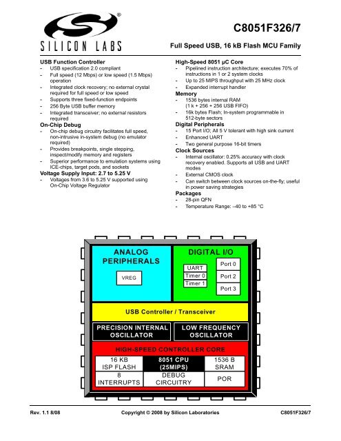
ANALOG<br />
PERIPHERALS<br />
VREG<br />
PRECISION INTERNAL<br />
OSCILLATOR<br />
16 KB<br />
ISP FLASH<br />
8<br />
INTERRUPTS<br />
<strong>C8051F326</strong>/7<br />
Full Speed USB, 16 kB Flash MCU Family<br />
8051 CPU<br />
(25MIPS)<br />
DEBUG<br />
CIRCUITRY<br />
High-Speed 8051 µC Core<br />
- Pipelined instruction architecture; executes 70% of<br />
instructions in 1 or 2 system clocks<br />
- Up to 25 MIPS throughput with 25 MHz clock<br />
- Expanded interrupt handler<br />
Memory<br />
- 1536 bytes internal RAM<br />
(1 k + 256 + 256 USB FIFO)<br />
- 16k bytes Flash; In-system programmable in<br />
512-byte sectors<br />
Digital Peripherals<br />
- 15 Port I/O; All 5 V tolerant with high sink current<br />
- Enhanced UART<br />
- Two general purpose 16-bit timers<br />
Clock Sources<br />
- Internal oscillator: 0.25% accuracy with clock<br />
recovery enabled. Supports all USB and UART<br />
modes<br />
- External CMOS clock<br />
- Can switch between clock sources on-the-fly; useful<br />
in power saving strategies<br />
Packages<br />
- 28-pin QFN<br />
- Temperature Range: –40 to +85 °C<br />
DIGITAL I/O<br />
UART<br />
Timer 0<br />
Timer 1<br />
USB Controller / Transceiver<br />
HIGH-SPEED CONTROLLER CORE<br />
Port 0<br />
Port 2<br />
Port 3<br />
LOW FREQUENCY<br />
OSCILLATOR<br />
1536 B<br />
SRAM<br />
Rev. 1.1 8/08 Copyright © 2008 by <strong>Silicon</strong> Laboratories <strong>C8051F326</strong>/7<br />
POR
<strong>C8051F326</strong>/7<br />
2 Rev. 1.1
Table of Contents<br />
<strong>C8051F326</strong>/7<br />
1. System Overview.................................................................................................... 13<br />
1.1. CIP-51 Microcontroller Core.......................................................................... 17<br />
1.1.1. Fully 8051 Compatible.............................................................................. 17<br />
1.1.2. Improved Throughput............................................................................... 17<br />
1.1.3. Additional Features .................................................................................. 18<br />
1.2. On-Chip Memory............................................................................................... 19<br />
1.3. Universal Serial Bus Controller ......................................................................... 20<br />
1.4. Voltage Regulator ............................................................................................. 20<br />
1.5. On-Chip Debug Circuitry................................................................................... 21<br />
1.6. Programmable Digital I/O.................................................................................. 22<br />
1.7. Serial Ports ....................................................................................................... 22<br />
2. Absolute Maximum Ratings .................................................................................. 23<br />
3. Global DC Electrical Characteristics .................................................................... 24<br />
4. Pinout and Package Definitions............................................................................ 25<br />
5. Voltage Regulator (REG0)...................................................................................... 31<br />
5.1. Regulator Mode Selection................................................................................. 31<br />
5.2. VBUS Detection ................................................................................................ 31<br />
6. CIP-51 Microcontroller .......................................................................................... 35<br />
6.1. Instruction Set ................................................................................................... 36<br />
6.1.1. Instruction and CPU Timing ..................................................................... 36<br />
6.1.2. MOVX Instruction and Program Memory ................................................. 37<br />
6.2. Memory Organization........................................................................................ 41<br />
6.2.1. Program Memory...................................................................................... 41<br />
6.2.2. Data Memory............................................................................................ 42<br />
6.2.3. General Purpose Registers ...................................................................... 42<br />
6.2.4. Bit Addressable Locations........................................................................ 42<br />
6.2.5. Stack ....................................................................................................... 42<br />
6.2.6. Special Function Registers....................................................................... 43<br />
6.2.7. Register Descriptions ............................................................................... 45<br />
6.3. Interrupt Handler ............................................................................................... 48<br />
6.3.1. MCU Interrupt Sources and Vectors ........................................................ 48<br />
6.3.2. External Interrupts.................................................................................... 49<br />
6.3.3. Interrupt Priorities..................................................................................... 49<br />
6.3.4. Interrupt Latency ...................................................................................... 49<br />
6.3.5. Interrupt Register Descriptions................................................................. 50<br />
6.4. Power Management Modes .............................................................................. 55<br />
6.4.1. Idle Mode.................................................................................................. 55<br />
6.4.2. Stop Mode................................................................................................ 55<br />
7. Reset Sources ....................................................................................................... 57<br />
7.1. Power-On Reset ............................................................................................... 58<br />
7.2. Power-Fail Reset / VDD Monitor....................................................................... 59<br />
7.3. External Reset .................................................................................................. 60<br />
7.4. Missing Clock Detector Reset........................................................................... 60<br />
Rev. 1.1 3
<strong>C8051F326</strong>/7<br />
7.5. Flash Error Reset.............................................................................................. 60<br />
7.6. Software Reset ................................................................................................. 60<br />
7.7. USB Reset ........................................................................................................ 60<br />
8. Flash Memory ....................................................................................................... 63<br />
8.1. Programming The Flash Memory ..................................................................... 63<br />
8.1.1. Flash Lock and Key Functions ................................................................. 63<br />
8.1.2. Flash Erase Procedure............................................................................. 63<br />
8.1.3. Flash Write Procedure.............................................................................. 64<br />
8.2. Non-volatile Data Storage................................................................................. 65<br />
8.3. Security Options................................................................................................ 65<br />
9. External RAM ........................................................................................................ 69<br />
9.1. Accessing User XRAM...................................................................................... 69<br />
9.2. Accessing USB FIFO Space............................................................................. 70<br />
10.Oscillators............................................................................................................... 71<br />
10.1.Programmable Internal Oscillator..................................................................... 71<br />
10.1.1.Adjusting the Internal Oscillator on <strong>C8051F326</strong>/7 Devices...................... 72<br />
10.1.2.Internal Oscillator Suspend Mode............................................................ 72<br />
10.2.Internal Low-Frequency (L-F) Oscillator........................................................... 74<br />
10.3.CMOS External Clock Input.............................................................................. 74<br />
10.4.4x Clock Multiplier ............................................................................................ 75<br />
10.5.System and USB Clock Selection .................................................................... 76<br />
10.5.1.System Clock Selection ........................................................................... 76<br />
10.5.2.USB Clock Selection................................................................................ 76<br />
11.Port Input/Output .................................................................................................. 79<br />
11.1.Port I/O Initialization ......................................................................................... 81<br />
11.2.General Purpose Port I/O................................................................................. 81<br />
12.Universal Serial Bus Controller (USB0)................................................................ 87<br />
12.1.Endpoint Addressing ........................................................................................ 88<br />
12.2.USB Transceiver .............................................................................................. 88<br />
12.3.USB Register Access ....................................................................................... 90<br />
12.4.USB Clock Configuration.................................................................................. 94<br />
12.5.FIFO Management ........................................................................................... 95<br />
12.5.1.FIFO Split Mode....................................................................................... 95<br />
12.5.2.FIFO Double Buffering ............................................................................. 95<br />
12.5.3.FIFO Access ............................................................................................ 96<br />
12.6.Function Addressing......................................................................................... 97<br />
12.7.Function Configuration and Control.................................................................. 98<br />
12.8.Interrupts ........................................................................................................ 101<br />
12.9.The Serial Interface Engine............................................................................ 104<br />
12.10. Endpoint0..................................................................................................... 104<br />
12.10.1.Endpoint0 SETUP Transactions .......................................................... 104<br />
12.10.2.Endpoint0 IN Transactions................................................................... 105<br />
12.10.3.Endpoint0 OUT Transactions............................................................... 105<br />
12.11.Configuring Endpoint1.................................................................................. 108<br />
4 Rev. 1.1
<strong>C8051F326</strong>/7<br />
12.12.Controlling Endpoint1 IN............................................................................... 108<br />
12.12.1.Endpoint1 IN Interrupt or Bulk Mode.................................................... 108<br />
12.12.2.Endpoint1 IN Isochronous Mode.......................................................... 108<br />
12.13.Controlling Endpoint1 OUT........................................................................... 112<br />
12.13.1.Endpoint1 OUT Interrupt or Bulk Mode................................................ 112<br />
12.13.2.Endpoint1 OUT Isochronous Mode...................................................... 112<br />
13.UART0.................................................................................................................... 117<br />
13.1.Baud Rate Generator ..................................................................................... 118<br />
13.2.Data Format.................................................................................................... 120<br />
13.3.Configuration and Operation .......................................................................... 121<br />
13.3.1.Data Transmission ................................................................................. 121<br />
13.3.2.Data Reception ...................................................................................... 121<br />
13.3.3.Multiprocessor Communications............................................................ 122<br />
14.Timers ................................................................................................................... 127<br />
14.1.Timer 0 and Timer 1 Operating Modes........................................................... 127<br />
14.1.1.Mode 0: 13-bit Timer.............................................................................. 128<br />
14.1.2.Mode 1: 16-bit Timer.............................................................................. 129<br />
14.1.3.Mode 2: 8-bit Timer with Auto-Reload.................................................... 129<br />
14.1.4.Mode 3: Two 8-bit Timers (Timer 0 Only) .............................................. 130<br />
15.C2 Interface........................................................................................................... 135<br />
15.1.C2 Interface Registers.................................................................................... 135<br />
15.2.C2 Pin Sharing ............................................................................................... 137<br />
Document Change List............................................................................................. 138<br />
Contact Information.................................................................................................. 140<br />
Rev. 1.1 5
<strong>C8051F326</strong>/7<br />
6 Rev. 1.1
List of Figures<br />
<strong>C8051F326</strong>/7<br />
1. System Overview<br />
Figure 1.1. <strong>C8051F326</strong> Block Diagram .................................................................... 14<br />
Figure 1.2. C8051F327 Block Diagram .................................................................... 15<br />
Figure 1.3. Typical Connections for the <strong>C8051F326</strong>................................................ 16<br />
Figure 1.4. Typical Connections for the C8051F327................................................ 16<br />
Figure 1.5. Comparison of Peak MCU Execution Speeds ....................................... 17<br />
Figure 1.6. On-Chip Clock and Reset ...................................................................... 18<br />
Figure 1.7. On-Board Memory Map.......................................................................... 19<br />
Figure 1.8. USB Controller Block Diagram............................................................... 20<br />
Figure 1.9. Development/In-System Debug Diagram............................................... 21<br />
2. Absolute Maximum Ratings<br />
3. Global DC Electrical Characteristics<br />
4. Pinout and Package Definitions<br />
Figure 4.1. <strong>C8051F326</strong> QFN-28 Pinout Diagram (Top View) .................................. 27<br />
Figure 4.2. C8051F327 QFN-28 Pinout Diagram (Top View) .................................. 28<br />
Figure 4.3. QFN-28 Package Drawing ..................................................................... 29<br />
Figure 4.4. QFN-28 Recommended PCB Land Pattern ........................................... 30<br />
5. Voltage Regulator (REG0)<br />
Figure 5.1. REG0 Configuration: USB Bus-Powered ............................................... 32<br />
Figure 5.2. REG0 Configuration: USB Self-Powered ............................................... 32<br />
Figure 5.3. REG0 Configuration: USB Self-Powered, Regulator Disabled .............. 33<br />
Figure 5.4. REG0 Configuration: No USB Connection............................................. 33<br />
6. CIP-51 Microcontroller<br />
Figure 6.1. CIP-51 Block Diagram............................................................................ 35<br />
Figure 6.2. Memory Map .......................................................................................... 41<br />
7. Reset Sources<br />
Figure 7.1. Reset Sources........................................................................................ 57<br />
Figure 7.2. Power-On and VDD Monitor Reset Timing ............................................ 58<br />
8. Flash Memory<br />
Figure 8.1. Flash Program Memory Map and Security Byte .................................... 66<br />
9. External RAM<br />
Figure 9.1. External Ram Memory Map ................................................................... 69<br />
Figure 9.2. XRAM Memory Map Expanded View..................................................... 70<br />
10.Oscillators<br />
Figure 10.1. Oscillator Diagram................................................................................ 71<br />
11.Port Input/Output<br />
Figure 11.1. Port I/O Functional Block Diagram....................................................... 79<br />
Figure 11.2. Port I/O Cell Block Diagram ................................................................. 80<br />
12.Universal Serial Bus Controller (USB0)<br />
Figure 12.1. USB0 Block Diagram............................................................................ 87<br />
Figure 12.2. USB0 Register Access Scheme........................................................... 90<br />
Figure 12.3. USB FIFO Allocation ............................................................................ 95<br />
13.UART0<br />
Figure 13.1. UART0 Block Diagram ....................................................................... 117<br />
Rev. 1.1 7
<strong>C8051F326</strong>/7<br />
Figure 13.2. UART0 Timing Without Parity or Extra Bit.......................................... 120<br />
Figure 13.3. UART0 Timing With Parity ................................................................. 120<br />
Figure 13.4. UART0 Timing With Extra Bit ............................................................. 120<br />
Figure 13.5. Typical UART Interconnect Diagram.................................................. 121<br />
Figure 13.6. UART Multi-Processor Mode Interconnect Diagram .......................... 122<br />
14.Timers<br />
Figure 14.1. T0 Mode 0 Block Diagram.................................................................. 128<br />
Figure 14.2. T0 Mode 2 Block Diagram.................................................................. 129<br />
Figure 14.3. T0 Mode 3 Block Diagram.................................................................. 130<br />
15.C2 Interface<br />
Figure 15.1. Typical C2 Pin Sharing....................................................................... 137<br />
8 Rev. 1.1
List of Tables<br />
<strong>C8051F326</strong>/7<br />
1. System Overview<br />
Table 1.1. Product Selection Guide ......................................................................... 13<br />
2. Absolute Maximum Ratings<br />
Table 2.1. Absolute Maximum Ratings .................................................................... 23<br />
3. Global DC Electrical Characteristics<br />
Table 3.1. Global DC Electrical Characteristics ....................................................... 24<br />
4. Pinout and Package Definitions<br />
Table 4.1. Pin Definitions for the <strong>C8051F326</strong>/7 ....................................................... 25<br />
Table 4.2. QFN-28 Package Dimensions ................................................................ 29<br />
Table 4.3. QFN-28 PCB Land Pattern Dimesions ................................................... 30<br />
5. Voltage Regulator (REG0)<br />
Table 5.1. Voltage Regulator Electrical Specifications . . . . . . . . . . . . . . . . . . . . . 31<br />
6. CIP-51 Microcontroller<br />
Table 6.1. CIP-51 Instruction Set Summary ............................................................ 37<br />
Table 6.2. Special Function Register (SFR) Memory Map ...................................... 43<br />
Table 6.3. Special Function Registers ..................................................................... 43<br />
Table 6.4. TMOD.3 Control of /INT0 ........................................................................ 49<br />
Table 6.5. Interrupt Summary .................................................................................. 50<br />
7. Reset Sources<br />
Table 7.1. Reset Electrical Characteristics . . . . . . . . . . . . . . . . . . . . . . . . . . . . . . 62<br />
8. Flash Memory<br />
Table 8.1. Flash Electrical Characteristics . . . . . . . . . . . . . . . . . . . . . . . . . . . . . . 64<br />
9. External RAM<br />
10.Oscillators<br />
Table 10.1. Typical USB Full Speed Clock Settings ................................................ 76<br />
Table 10.2. Typical USB Low Speed Clock Settings ............................................... 76<br />
Table 10.3. Internal Oscillator Electrical Characteristics . . . . . . . . . . . . . . . . . . . . 78<br />
11.Port Input/Output<br />
Table 11.1. Port I/O DC Electrical Characteristics (<strong>C8051F326</strong>) . . . . . . . . . . . . . 85<br />
Table 11.2. Port I/O DC Electrical Characteristics (C8051F327) . . . . . . . . . . . . . 85<br />
12.Universal Serial Bus Controller (USB0)<br />
Table 12.1. Endpoint Addressing Scheme .............................................................. 88<br />
Table 12.2. USB0 Controller Registers ................................................................... 93<br />
Table 12.3. FIFO Configurations ............................................................................. 95<br />
Table 12.4. USB Transceiver Electrical Characteristics . . . . . . . . . . . . . . . . . . . 115<br />
13.UART0<br />
Table 13.1. Baud Rate Generator Settings for Standard Baud Rates ................... 119<br />
14.Timers<br />
Table 14.1. Timer Modes ....................................................................................... 127<br />
Table 14.2. Timer 0 Operation ............................................................................... 128<br />
15.C2 Interface<br />
Rev. 1.1 9
<strong>C8051F326</strong>/7<br />
10 Rev. 1.1
List of Registers<br />
<strong>C8051F326</strong>/7<br />
SFR Definition 5.1. REG0CN: Voltage Regulator Control . . . . . . . . . . . . . . . . . . . . . . 34<br />
SFR Definition 6.1. DPL: Data Pointer Low Byte . . . . . . . . . . . . . . . . . . . . . . . . . . . . . 45<br />
SFR Definition 6.2. DPH: Data Pointer High Byte . . . . . . . . . . . . . . . . . . . . . . . . . . . . . 45<br />
SFR Definition 6.3. SP: Stack Pointer . . . . . . . . . . . . . . . . . . . . . . . . . . . . . . . . . . . . . . 45<br />
SFR Definition 6.4. PSW: Program Status Word . . . . . . . . . . . . . . . . . . . . . . . . . . . . . 46<br />
SFR Definition 6.5. ACC: Accumulator . . . . . . . . . . . . . . . . . . . . . . . . . . . . . . . . . . . . . 46<br />
SFR Definition 6.6. B: B Register . . . . . . . . . . . . . . . . . . . . . . . . . . . . . . . . . . . . . . . . . 47<br />
SFR Definition 6.7. IE: Interrupt Enable . . . . . . . . . . . . . . . . . . . . . . . . . . . . . . . . . . . . 51<br />
SFR Definition 6.8. IP: Interrupt Priority . . . . . . . . . . . . . . . . . . . . . . . . . . . . . . . . . . . . 52<br />
SFR Definition 6.9. EIE1: Extended Interrupt Enable 1 . . . . . . . . . . . . . . . . . . . . . . . . 53<br />
SFR Definition 6.10. EIP1: Extended Interrupt Priority 1 . . . . . . . . . . . . . . . . . . . . . . . 53<br />
SFR Definition 6.11. EIE2: Extended Interrupt Enable 2 . . . . . . . . . . . . . . . . . . . . . . . 53<br />
SFR Definition 6.12. EIP2: Extended Interrupt Priority 2 . . . . . . . . . . . . . . . . . . . . . . . 54<br />
SFR Definition 6.13. PCON: Power Control . . . . . . . . . . . . . . . . . . . . . . . . . . . . . . . . . 56<br />
SFR Definition 7.1. VDM0CN: VDD Monitor Control . . . . . . . . . . . . . . . . . . . . . . . . . . 59<br />
SFR Definition 7.2. RSTSRC: Reset Source . . . . . . . . . . . . . . . . . . . . . . . . . . . . . . . . 61<br />
SFR Definition 8.1. PSCTL: Program Store R/W Control . . . . . . . . . . . . . . . . . . . . . . . 66<br />
SFR Definition 8.2. FLKEY: Flash Lock and Key . . . . . . . . . . . . . . . . . . . . . . . . . . . . . 67<br />
SFR Definition 8.3. FLSCL: Flash Scale . . . . . . . . . . . . . . . . . . . . . . . . . . . . . . . . . . . . 67<br />
SFR Definition 9.1. EMI0CN: External Memory Interface Control . . . . . . . . . . . . . . . . 70<br />
SFR Definition 10.1. OSCICN: Internal Oscillator Control . . . . . . . . . . . . . . . . . . . . . . 72<br />
SFR Definition 10.2. OSCICL: Internal Oscillator Calibration . . . . . . . . . . . . . . . . . . . . 73<br />
SFR Definition 10.3. OSCLCN: Internal L-F Oscillator Control . . . . . . . . . . . . . . . . . . . 74<br />
SFR Definition 10.4. CLKMUL: Clock Multiplier Control . . . . . . . . . . . . . . . . . . . . . . . . 75<br />
SFR Definition 10.5. CLKSEL: Clock Select . . . . . . . . . . . . . . . . . . . . . . . . . . . . . . . . 77<br />
SFR Definition 11.1. GPIOCN: Global Port I/O Control . . . . . . . . . . . . . . . . . . . . . . . . 82<br />
SFR Definition 11.2. P0: Port0 . . . . . . . . . . . . . . . . . . . . . . . . . . . . . . . . . . . . . . . . . . . 82<br />
SFR Definition 11.3. P0MDOUT: Port0 Output Mode . . . . . . . . . . . . . . . . . . . . . . . . . . 82<br />
SFR Definition 11.4. P2: Port2 . . . . . . . . . . . . . . . . . . . . . . . . . . . . . . . . . . . . . . . . . . . 83<br />
SFR Definition 11.5. P2MDOUT: Port2 Output Mode . . . . . . . . . . . . . . . . . . . . . . . . . . 83<br />
SFR Definition 11.6. P3: Port3 . . . . . . . . . . . . . . . . . . . . . . . . . . . . . . . . . . . . . . . . . . . 83<br />
SFR Definition 11.7. P3MDOUT: Port3 Output Mode . . . . . . . . . . . . . . . . . . . . . . . . . . 84<br />
USB Register Definition 12.1. USB0XCN: USB0 Transceiver Control . . . . . . . . . . . . . 89<br />
USB Register Definition 12.2. USB0ADR: USB0 Indirect Address . . . . . . . . . . . . . . . . 91<br />
USB Register Definition 12.3. USB0DAT: USB0 Data . . . . . . . . . . . . . . . . . . . . . . . . . 92<br />
USB Register Definition 12.4. INDEX: USB0 Endpoint Index . . . . . . . . . . . . . . . . . . . . 92<br />
USB Register Definition 12.5. CLKREC: Clock Recovery Control . . . . . . . . . . . . . . . . 94<br />
USB Register Definition 12.6. FIFOn: USB0 Endpoint FIFO Access . . . . . . . . . . . . . . 96<br />
USB Register Definition 12.7. FADDR: USB0 Function Address . . . . . . . . . . . . . . . . . 97<br />
USB Register Definition 12.8. POWER: USB0 Power . . . . . . . . . . . . . . . . . . . . . . . . . 99<br />
USB Register Definition 12.9. FRAMEL: USB0 Frame Number Low . . . . . . . . . . . . . 100<br />
USB Register Definition 12.10. FRAMEH: USB0 Frame Number High . . . . . . . . . . . 100<br />
USB Register Definition 12.11. IN1INT: USB0 IN Endpoint Interrupt . . . . . . . . . . . . . 101<br />
Rev. 1.1 11
<strong>C8051F326</strong>/7<br />
USB Register Definition 12.12. OUT1INT: USB0 Out Endpoint Interrupt . . . . . . . . . . 101<br />
USB Register Definition 12.13. CMINT: USB0 Common Interrupt . . . . . . . . . . . . . . . 102<br />
USB Register Definition 12.14. IN1IE: USB0 IN Endpoint Interrupt Enable . . . . . . . . 102<br />
USB Register Definition 12.15. OUT1IE: USB0 Out Endpoint Interrupt Enable . . . . . 103<br />
USB Register Definition 12.16. CMIE: USB0 Common Interrupt Enable . . . . . . . . . . 103<br />
USB Register Definition 12.17. E0CSR: USB0 Endpoint0 Control . . . . . . . . . . . . . . . 106<br />
USB Register Definition 12.18. E0CNT: USB0 Endpoint 0 Data Count . . . . . . . . . . . 107<br />
USB Register Definition 12.19. EINCSRL: USB0 IN Endpoint Control Low Byte . . . . 110<br />
USB Register Definition 12.20. EINCSRH: USB0 IN Endpoint Control High Byte . . . 111<br />
USB Register Definition 12.21. EOUTCSRL: USB0 OUT Endpoint Control Low Byte 113<br />
USB Register Definition 12.22. EOUTCSRH: USB0 OUT<br />
Endpoint Control High Byte . . . . . . . . . . . . . . . . . . . . 114<br />
USB Register Definition 12.23. EOUTCNTL: USB0 OUT Endpoint Count Low . . . . . 114<br />
USB Register Definition 12.24. EOUTCNTH: USB0 OUT Endpoint Count High . . . . 114<br />
SFR Definition 13.1. SCON0: UART0 Control . . . . . . . . . . . . . . . . . . . . . . . . . . . . . . 123<br />
SFR Definition 13.2. SMOD0: UART0 Mode . . . . . . . . . . . . . . . . . . . . . . . . . . . . . . . 124<br />
SFR Definition 13.3. SBUF0: UART0 Data Buffer . . . . . . . . . . . . . . . . . . . . . . . . . . . 125<br />
SFR Definition 13.4. SBCON0: UART0 Baud Rate Generator Control . . . . . . . . . . . 125<br />
SFR Definition 13.5. SBRLH0: UART0 Baud Rate Generator High Byte . . . . . . . . . . 126<br />
SFR Definition 13.6. SBRLL0: UART0 Baud Rate Generator Low Byte . . . . . . . . . . . 126<br />
SFR Definition 14.1. TCON: Timer Control . . . . . . . . . . . . . . . . . . . . . . . . . . . . . . . . . 131<br />
SFR Definition 14.2. TMOD: Timer Mode . . . . . . . . . . . . . . . . . . . . . . . . . . . . . . . . . . 132<br />
SFR Definition 14.3. CKCON: Clock Control . . . . . . . . . . . . . . . . . . . . . . . . . . . . . . . 133<br />
SFR Definition 14.4. TL0: Timer 0 Low Byte . . . . . . . . . . . . . . . . . . . . . . . . . . . . . . . . 134<br />
SFR Definition 14.5. TL1: Timer 1 Low Byte . . . . . . . . . . . . . . . . . . . . . . . . . . . . . . . . 134<br />
SFR Definition 14.6. TH0: Timer 0 High Byte . . . . . . . . . . . . . . . . . . . . . . . . . . . . . . . 134<br />
SFR Definition 14.7. TH1: Timer 1 High Byte . . . . . . . . . . . . . . . . . . . . . . . . . . . . . . . 134<br />
C2 Register Definition 15.1. C2ADD: C2 Address . . . . . . . . . . . . . . . . . . . . . . . . . . . 135<br />
C2 Register Definition 15.2. DEVICEID: C2 Device ID . . . . . . . . . . . . . . . . . . . . . . . . 135<br />
C2 Register Definition 15.3. REVID: C2 Revision ID . . . . . . . . . . . . . . . . . . . . . . . . . 136<br />
C2 Register Definition 15.4. FPCTL: C2 Flash Programming Control . . . . . . . . . . . . 136<br />
C2 Register Definition 15.5. FPDAT: C2 Flash Programming Data . . . . . . . . . . . . . . 136<br />
12 Rev. 1.1
1. System Overview<br />
<strong>C8051F326</strong>/7<br />
<strong>C8051F326</strong>/7 devices are fully integrated mixed-signal system-on-a-chip MCUs. Highlighted features are<br />
listed below. Refer to Table 1.1 for specific product feature selection.<br />
• High-speed pipelined 8051-compatible microcontroller core (up to 25 MIPS)<br />
• In-system, full-speed, non-intrusive debug interface (on-chip)<br />
• Universal serial bus (USB) function controller with three fixed-function endpoint pipes, integrated transceiver,<br />
and 256B FIFO RAM<br />
• Supply voltage regulator<br />
• Precision programmable 12 MHz internal oscillator and 4x clock multiplier<br />
• 16k kB of on-chip Flash memory<br />
• 1536 total bytes of on-chip RAM (256 + 1 k + 256 USB FIFO)<br />
• Enhanced UART, serial interfaces implemented in hardware<br />
• Two general-purpose 16-bit timers<br />
• On-chip power-on reset, VDD monitor, and missing clock detector<br />
• 15 Port I/O (5 V tolerant)<br />
With on-chip power-on reset, VDD monitor, voltage regulator, and clock oscillator, <strong>C8051F326</strong>/7 devices<br />
are truly stand-alone System-on-a-Chip solutions. The Flash memory can be reprogrammed in-circuit, providing<br />
non-volatile data storage, and also allowing field upgrades of the 8051 firmware. User software has<br />
complete control of all peripherals, and may individually shut down any or all peripherals for power savings.<br />
The on-chip <strong>Silicon</strong> Laboratories 2-Wire (C2) Development Interface allows non-intrusive (uses no on-chip<br />
resources), full speed, in-circuit debugging using the production MCU installed in the final application. This<br />
debug logic supports inspection and modification of memory and registers, setting breakpoints, single<br />
stepping, run and halt commands. All analog and digital peripherals are fully functional while debugging<br />
using C2. The two C2 interface pins can be shared with user functions, allowing in-system debugging without<br />
occupying package pins.<br />
Each device is specified for 2.7–5.25 V operation over the industrial temperature range (–40 to +85 °C).<br />
For voltages above 3.6 V, the on-chip Voltage Regulator must be used. A minimum of 3.0 V is required for<br />
USB communication. The Port I/O and RST pins are tolerant of input signals up to 5 V. <strong>C8051F326</strong>/7 are<br />
available in two 28-pin QFN packages with different pinouts. The RoHS compliant devices are marked with<br />
a -GM suffix in the part number. The port I/O on <strong>C8051F326</strong> devices is powered from a separate I/O supply<br />
allowing it to interface to low voltage logic.<br />
Ordering Part<br />
Number<br />
MIPS (Peak)<br />
Table 1.1. Product Selection Guide<br />
Flash Memory<br />
RAM<br />
Calibrated Internal<br />
Oscillator<br />
USB<br />
Supply Voltage<br />
Regulator<br />
<strong>C8051F326</strong>-GM 25 16k 1536 2 15 QFN-28<br />
C8051F327-GM 25 16k 1536 2 15 — QFN-28<br />
UART<br />
Timers (16-bit)<br />
Digital Port I/Os<br />
Separate I/O Supply<br />
Package<br />
Rev. 1.1 13
<strong>C8051F326</strong>/7<br />
REGIN<br />
VDD<br />
GND<br />
/RST/C2CK<br />
D+<br />
D-<br />
VBUS<br />
XTAL2<br />
Analog/Digital<br />
Power<br />
C2D<br />
Low Freq<br />
Oscillator<br />
12 MHz<br />
Internal<br />
Oscillator<br />
Clock<br />
Recovery<br />
5.0 V Voltage<br />
IN<br />
Regulator<br />
OUT<br />
POR<br />
Debug HW<br />
Brown-<br />
Out<br />
x4 2<br />
2<br />
XTAL2<br />
1,2,3,4<br />
USB<br />
Transceiver<br />
Enable<br />
USB Clock<br />
Reset<br />
System<br />
Clock<br />
USB<br />
Controller<br />
256 byte<br />
USB SRAM<br />
16 kB<br />
FLASH<br />
256 byte<br />
SRAM<br />
SFR Bus<br />
Figure 1.1. <strong>C8051F326</strong> Block Diagram<br />
14 Rev. 1.1<br />
8<br />
0<br />
5<br />
1<br />
C<br />
o<br />
r<br />
e<br />
1 kB<br />
XRAM<br />
Port 0<br />
Latch<br />
UART<br />
/SYSCLK<br />
Timer 0,1<br />
Port 2<br />
Latch<br />
Port 3<br />
Latch<br />
P<br />
0<br />
D<br />
r<br />
v<br />
P<br />
2<br />
D<br />
r<br />
v<br />
P<br />
3<br />
D<br />
r<br />
v<br />
VIO<br />
P0.0/SYSCLK<br />
P0.1<br />
P0.2<br />
P0.3/XTAL2<br />
P0.4/TX<br />
P0.5/RX<br />
P0.6<br />
P0.7<br />
P2.0<br />
P2.1<br />
P2.2<br />
P2.3<br />
P2.4<br />
P2.5<br />
P3.0/C2D
REGIN<br />
VDD<br />
GND<br />
/RST/C2CK<br />
D+<br />
D-<br />
VBUS<br />
XTAL2<br />
Analog/Digital<br />
Power<br />
C2D<br />
Low Freq<br />
Oscillator<br />
12 MHz<br />
Internal<br />
Oscillator<br />
Clock<br />
Recovery<br />
5.0 V Voltage<br />
IN<br />
Regulator<br />
OUT<br />
POR<br />
Debug HW<br />
Brown-<br />
Out<br />
x4 2<br />
1,2,3,4<br />
2<br />
XTAL2<br />
USB<br />
Transceiver<br />
Enable<br />
USB Clock<br />
Reset<br />
System<br />
Clock<br />
USB<br />
Controller<br />
256 byte<br />
USB SRAM<br />
8<br />
0<br />
5<br />
1<br />
C<br />
o<br />
r<br />
e<br />
16 kB<br />
FLASH<br />
256 byte<br />
SRAM<br />
1 kB<br />
XRAM<br />
SFR Bus<br />
Port 0<br />
Latch<br />
UART<br />
/SYSCLK<br />
Timer 0,1<br />
Port 2<br />
Latch<br />
Port 3<br />
Latch<br />
Figure 1.2. C8051F327 Block Diagram<br />
<strong>C8051F326</strong>/7<br />
Rev. 1.1 15<br />
P<br />
0<br />
D<br />
r<br />
v<br />
P<br />
2<br />
D<br />
r<br />
v<br />
P<br />
3<br />
D<br />
r<br />
v<br />
P0.0/SYSCLK<br />
P0.1<br />
P0.2<br />
P0.3/XTAL2<br />
P0.4/TX<br />
P0.5/RX<br />
P0.6<br />
P0.7<br />
P2.0<br />
P2.1<br />
P2.2<br />
P2.3<br />
P2.4<br />
P2.5<br />
P3.0/C2D
<strong>C8051F326</strong>/7<br />
Figure 1.3. Typical Connections for the <strong>C8051F326</strong><br />
Figure 1.4. Typical Connections for the C8051F327<br />
16 Rev. 1.1
1.1. CIP-51 Microcontroller Core<br />
1.1.1. Fully 8051 Compatible<br />
<strong>C8051F326</strong>/7<br />
The <strong>C8051F326</strong>/7 family utilizes <strong>Silicon</strong> Laboratories' proprietary CIP-51 microcontroller core. The CIP-51<br />
is fully compatible with the MCS-51 instruction set; standard 803x/805x assemblers and compilers can<br />
be used to develop software. The CIP-51 core offers all the peripherals included with a standard 8052,<br />
including two 16-bit counter/timers, a full-duplex UART with extended baud rate configuration, 1536 bytes<br />
of on-chip RAM, 128 byte Special Function Register (SFR) address space, and 15 I/O pins.<br />
1.1.2. Improved Throughput<br />
The CIP-51 employs a pipelined architecture that greatly increases its instruction throughput over the standard<br />
8051 architecture. In a standard 8051, all instructions except for MUL and DIV take 12 or 24 system<br />
clock cycles to execute with a maximum system clock of 12-to-24 MHz. By contrast, the CIP-51 core executes<br />
70% of its instructions in one or two system clock cycles, with only four instructions taking more than<br />
four system clock cycles.<br />
The CIP-51 has a total of 109 instructions. The table below shows the total number of instructions that<br />
require each execution time.<br />
Clocks to Execute 1 2 2/3 3 3/4 4 4/5 5 8<br />
Number of Instructions 26 50 5 14 7 3 1 2 1<br />
With the CIP-51's maximum system clock at 25 MHz, it has a peak throughput of 25 MIPS. Figure 1.5<br />
shows a comparison of peak throughputs for various 8-bit microcontroller cores with their maximum system<br />
clocks.<br />
MIPS<br />
25<br />
20<br />
15<br />
10<br />
5<br />
<strong>Silicon</strong> <strong>Labs</strong><br />
CIP-51<br />
(25 MHz clk)<br />
Microchip<br />
PIC17C75x<br />
(33 MHz clk)<br />
Philips<br />
80C51<br />
(33 MHz clk)<br />
ADuC812<br />
8051<br />
(16 MHz clk)<br />
Figure 1.5. Comparison of Peak MCU Execution Speeds<br />
Rev. 1.1 17
<strong>C8051F326</strong>/7<br />
1.1.3. Additional Features<br />
The <strong>C8051F326</strong>/7 SoC family includes several key enhancements to the CIP-51 core and peripherals to<br />
improve performance and ease of use in end applications.<br />
The extended interrupt handler provides 8 interrupt sources into the CIP-51. An interrupt driven system<br />
requires less intervention by the MCU, giving it more effective throughput. The interrupt sources are very<br />
useful when building multi-tasking, real-time systems.<br />
Seven reset sources are available: power-on reset circuitry (POR), an on-chip VDD monitor (forces reset<br />
when power supply voltage drops below V RST as given in Table 7.1 on page 62), the USB controller (USB<br />
bus reset or a VBUS transition), a Missing Clock Detector, a forced software reset, an external reset pin,<br />
and an errant Flash read/write protection circuit. Each reset source except for the POR, Reset Input Pin, or<br />
Flash error may be disabled by the user in software.<br />
The internal oscillator is factory calibrated to 12 MHz ±1.5%, and the internal oscillator period may be user<br />
programmed in ~0.25% increments. An additional low-frequency oscillator is also available which facilitates<br />
low power operation. A clock recovery mechanism allows the internal oscillator to be used with the 4x<br />
Clock Multiplier as the USB clock source in Full Speed mode; the internal oscillator can also be used as<br />
the USB clock source in Low Speed mode. An external CMOS clock may also be used with the 4x Clock<br />
Multiplier. The system clock may be configured to use the internal oscillator, external clock, low-frequency<br />
oscillator, or the Clock Multiplier output divided by 2. If desired, the system clock source may be switched<br />
on-the-fly between oscillator sources. The external clock and internal low-frequency oscillator can be<br />
extremely useful in low power applications, allowing the MCU to run from a slow (power saving) clock<br />
source, while periodically switching to the high-frequency internal oscillator as needed.<br />
XTAL2<br />
Low<br />
Frequency<br />
Oscillator<br />
Internal<br />
Oscillator<br />
External<br />
Clock Input<br />
System<br />
Clock<br />
Clock Select<br />
Missing<br />
Clock<br />
Detector<br />
(oneshot)<br />
(Software Reset)<br />
EN<br />
SWRSF<br />
CIP-51<br />
Microcontroller<br />
Core<br />
Extended Interrupt<br />
Handler<br />
Figure 1.6. On-Chip Clock and Reset<br />
18 Rev. 1.1<br />
MCD<br />
Enable<br />
VDD<br />
Supply<br />
Monitor<br />
+<br />
-<br />
System Reset<br />
Enable<br />
Power On<br />
Reset<br />
'0'<br />
Errant<br />
FLASH<br />
Operation<br />
(wired-OR)<br />
Reset<br />
Funnel<br />
/RST
1.2. On-Chip Memory<br />
<strong>C8051F326</strong>/7<br />
The CIP-51 has a standard 8051 program and data address configuration. It includes 256 bytes of data<br />
RAM, with the upper 128 bytes dual-mapped. Indirect addressing accesses the upper 128 bytes of general<br />
purpose RAM, and direct addressing accesses the 128 byte SFR address space. The lower 128 bytes of<br />
RAM are accessible via direct and indirect addressing. The first 32 bytes are addressable as four banks of<br />
general purpose registers, and the next 16 bytes can be byte addressable or bit addressable.<br />
Program memory consists of 16k bytes of Flash. This memory may be reprogrammed in-system in 512<br />
byte sectors, and requires no special off-chip programming voltage. See Figure 1.7 for the MCU system<br />
memory map.<br />
PROGRAM/DATA MEMORY<br />
(FLASH)<br />
0x3FFF<br />
RESERVED<br />
0x3E00<br />
0x3DFF<br />
0x0000<br />
16K FLASH<br />
(In-System<br />
Programmable in 512<br />
Byte Sectors)<br />
0xFF<br />
0x80<br />
0x7F<br />
0x30<br />
0x2F<br />
0x20<br />
0x1F<br />
0x00<br />
0xFFFF<br />
0x0400<br />
0x03FF<br />
0x0000<br />
DATA MEMORY (RAM)<br />
INTERNAL DATA ADDRESS SPACE<br />
Upper 128 RAM<br />
(Indirect Addressing<br />
Only)<br />
(Direct and Indirect<br />
Addressing)<br />
Bit Addressable<br />
General Purpose<br />
Registers<br />
Same 1024 bytes as from<br />
0x0000 to 0x03FF, wrapped<br />
on 1K-byte boundaries<br />
Figure 1.7. On-Board Memory Map<br />
Special Function<br />
Register's<br />
(Direct Addressing Only)<br />
Lower 128 RAM<br />
(Direct and Indirect<br />
Addressing)<br />
EXTERNAL DATA ADDRESS SPACE<br />
XRAM - 1024 Bytes<br />
(accessable using MOVX<br />
instruction)<br />
USB FIFOs<br />
256 Bytes<br />
Accessible through<br />
USB Registers Only<br />
Rev. 1.1 19
<strong>C8051F326</strong>/7<br />
1.3. Universal Serial Bus Controller<br />
The Universal Serial Bus Controller (USB0) is a USB 2.0 peripheral with integrated transceiver and endpoint<br />
FIFO RAM. The controller supports both full and low speed modes. A total of three endpoint pipes are<br />
available: a bi-directional control endpoint (Endpoint0) and a data endpoint (Endpoint1) with one IN pipe<br />
and one OUT pipe.<br />
A 256 block of XRAM is used as dedicated USB FIFO space. This FIFO space is distributed between<br />
Endpoint0 and Endpoint1. Endpoint0 is 64 bytes, and Endpoint1 has a 64 byte IN pipe and a 128 byte OUT<br />
pipe.<br />
USB0 can be operated as a Full or Low Speed function. The on-chip 4x Clock Multiplier and clock recovery<br />
circuitry allow both Full and Low Speed options to be implemented with the on-chip precision oscillator as<br />
the USB clock source. An external clock source can also be used with the 4x Clock Multiplier to generate<br />
the USB clock.<br />
The USB Transceiver is USB 2.0 compliant, and includes on-chip matching and pullup resistors. The pullup<br />
resistors can be enabled/disabled in software, and will appear on the D+ or D– pin according to the<br />
software-selected speed setting (full or low speed).<br />
D+<br />
D-<br />
VDD<br />
Transceiver Serial Interface Engine (SIE)<br />
1.4. Voltage Regulator<br />
Data<br />
Transfer<br />
Control<br />
Endpoint0<br />
IN/OUT<br />
Endpoint1<br />
IN OUT<br />
USB FIFOs<br />
(256B RAM)<br />
Figure 1.8. USB Controller Block Diagram<br />
<strong>C8051F326</strong>/7 devices include a voltage regulator (REG0). When enabled, the REG0 output appears on<br />
the VDD pin and can be used to power external devices. REG0 can be enabled/disabled by software.<br />
20 Rev. 1.1<br />
USB<br />
Control,<br />
Status, and<br />
Interrupt<br />
Registers<br />
CIP-51 Core
1.5. On-Chip Debug Circuitry<br />
<strong>C8051F326</strong>/7<br />
<strong>C8051F326</strong>/7 devices include on-chip <strong>Silicon</strong> Laboratories 2-Wire (C2) debug circuitry that provides nonintrusive,<br />
full speed, in-circuit debugging of the production part installed in the end application.<br />
The <strong>Silicon</strong> Laboratories' debugging system supports inspection and modification of memory and registers,<br />
breakpoints, and single stepping. No additional target RAM, program memory, timers, or communications<br />
channels are required. All the digital and analog peripherals are functional and work correctly while debugging.<br />
All the peripherals (except for the USB) are stalled when the MCU is halted, during single stepping, or<br />
at a breakpoint in order to keep them synchronized.<br />
The <strong>C8051F326</strong>DK development kit provides all the hardware and software necessary to develop application<br />
code and perform in-circuit debugging with the <strong>C8051F326</strong>/7 MCUs. The kit includes a Windows<br />
development environment, a serial adapter for connecting to the C2 port, and a target application board.<br />
All of the necessary communication cables and a wall-mount power supply are also supplied with the<br />
development kit. The <strong>Silicon</strong> Laboratories debug environment is a vastly superior configuration for developing<br />
and debugging embedded applications compared to standard MCU emulators, which use on-board<br />
"ICE Chips" and target cables and require the MCU in the application board to be socketed. The <strong>Silicon</strong><br />
Laboratories debug environment enhances ease of use and preserves the performance of on-chip peripherals.<br />
WINDOWS PC<br />
<strong>Silicon</strong> Laboratories Integrated<br />
Development Environment<br />
C2 (x2), VDD, GND<br />
VDD GND<br />
<strong>C8051F326</strong><br />
Serial<br />
Adapter<br />
TARGET PCB<br />
Figure 1.9. Development/In-System Debug Diagram<br />
Rev. 1.1 21
<strong>C8051F326</strong>/7<br />
1.6. Programmable Digital I/O<br />
<strong>C8051F326</strong>/7 devices include 15 I/O pins (one byte-wide Port, one 6-bit-wide and one 1-bit-wide Port).<br />
The <strong>C8051F326</strong>/7 Ports behave like typical 8051 Ports with a few enhancements. Each Port pin may be<br />
configured as a digital input or output pin. Pins selected as digital outputs may additionally be configured<br />
for push-pull or open-drain output. The “weak pullups” that are fixed on typical 8051 devices may be globally<br />
disabled, providing power savings capabilities.<br />
1.7. Serial Ports<br />
The <strong>C8051F326</strong>/7 Family includes a full-duplex UART with enhanced baud rate configuration. The serial<br />
interface is fully implemented in hardware and makes extensive use of the CIP-51's interrupts, thus requiring<br />
very little CPU intervention.<br />
22 Rev. 1.1
2. Absolute Maximum Ratings<br />
Table 2.1. Absolute Maximum Ratings<br />
<strong>C8051F326</strong>/7<br />
Parameter Conditions Min Typ Max Units<br />
Ambient Temperature under Bias –55 — 125 °C<br />
Storage Temperature –65 — 150 °C<br />
Voltage on any Port I/O Pin or RST with<br />
Respect to GND<br />
–0.3 — 5.8 V<br />
Voltage on VDD or VIO with Respect to GND –0.3 — 4.2 V<br />
Maximum Total Current through VDD, VIO,<br />
and GND<br />
Maximum Output Current Sunk by RST or<br />
any Port Pin<br />
— — 500 mA<br />
— — 100 mA<br />
Note: Stresses above those listed under “Absolute Maximum Ratings” may cause permanent damage to the device.<br />
This is a stress rating only and functional operation of the devices at those or any other conditions above<br />
those indicated in the operation listings of this specification is not implied. Exposure to maximum rating<br />
conditions for extended periods may affect device reliability.<br />
Rev. 1.1 23
<strong>C8051F326</strong>/7<br />
3. Global DC Electrical Characteristics<br />
Table 3.1. Global DC Electrical Characteristics<br />
–40 to +85 °C, 25 MHz System Clock unless otherwise specified.<br />
Parameter Conditions Min Typ Max Units<br />
I/O Supply Voltage (VIO) 1,2 1.8 3.3 3.6 V<br />
Core Supply Voltage (VDD) 3 2.7 3.3 3.6 V<br />
Core Supply Current with CPU<br />
Active<br />
Core Supply Current with CPU<br />
Inactive (not accessing Flash)<br />
Digital Supply Current (suspend<br />
mode or shutdown mode)<br />
Digital Supply RAM Data Retention<br />
Voltage<br />
VDD = 3.3 V, Clock = 24 MHz<br />
VDD = 3.3 V, Clock = 3 MHz<br />
VDD = 3.3 V, Clock = 32 kHz<br />
VDD = 3.3 V, Clock = 24 MHz<br />
VDD = 3.3 V, Clock = 3 MHz<br />
VDD = 3.3 V, Clock = 32 kHz<br />
Oscillator not running<br />
24 Rev. 1.1<br />
—<br />
—<br />
—<br />
—<br />
—<br />
—<br />
11<br />
1.9<br />
20<br />
4.4<br />
0.83<br />
13<br />
—<br />
—<br />
—<br />
—<br />
—<br />
—<br />
mA<br />
mA<br />
µA<br />
mA<br />
mA<br />
µA<br />
— < 0.1 — µA<br />
— 1.5 — V<br />
SYSCLK (System Clock) 4 0 — 25 MHz<br />
T SYSH (SYSCLK High Time) 18 — — ns<br />
T SYSL (SYSCLK Low Time) 18 — — ns<br />
Specified Operating Temperature<br />
Range<br />
–40 — +85 °C<br />
Notes:<br />
1. The I/O Supply Voltage (VIO) must be less than or equal to the Core Supply Voltage (VDD).<br />
2. For C8051F327 devices, VIO is internally connected to VDD.<br />
3. USB Requires 3.0 V Minimum Core Supply Voltage (VDD).<br />
4. SYSCLK must be at least 32 kHz to enable debugging.
4. Pinout and Package Definitions<br />
Name<br />
Table 4.1. Pin Definitions for the <strong>C8051F326</strong>/7<br />
Pin Numbers<br />
‘F326 ‘F327<br />
VDD 6 6<br />
VIO<br />
5 —<br />
Type Description<br />
Power<br />
In<br />
Power<br />
Out<br />
Power<br />
In<br />
GND 2 3 Ground.<br />
RST/<br />
C2CK<br />
P3.0/<br />
C2D<br />
REGIN<br />
9 9<br />
10 10<br />
7 7<br />
D I/O<br />
D I/O<br />
D I/O<br />
D I/O<br />
Power<br />
In<br />
VBUS 8 8 D In<br />
D+ 3 4 D I/O USB D+.<br />
D– 4 5 D I/O USB D–.<br />
2.7–3.6 V Core Supply Voltage Input.<br />
<strong>C8051F326</strong>/7<br />
3.3 V Voltage Regulator Output. See Section 5.<br />
V I/O Supply Voltage Input. The voltage at this pin must be<br />
less than or equal to the Core Supply Voltage (V DD ) for the<br />
'F326. On the 'F327, this pin is internally connected to V DD .<br />
Device Reset. Open-drain output of internal POR or VDD<br />
monitor. An external source can initiate a system reset by<br />
driving this pin low for at least 15 µs. See Section 7.<br />
Clock signal for the C2 Debug Interface.<br />
Port 3.0. See Section 11 for a complete description.<br />
Bi-directional data signal for the C2 Debug Interface.<br />
5 V Regulator Input. This pin is the input to the on-chip voltage<br />
regulator.<br />
VBUS Sense Input. This pin should be connected to the<br />
VBUS signal of a USB network. A 5 V signal on this pin indicates<br />
a USB network connection.<br />
P0.0 1 2 D I/O Port 0.0. See Section 11 for a complete description.<br />
P0.1 28 1 D I/O Port 0.1. See Section 11 for a complete description.<br />
P0.2 27 28 D I/O Port 0.2. See Section 11 for a complete description.<br />
P0.3/<br />
XTAL2<br />
26 27<br />
D I/O<br />
D In<br />
Port 0.3. See Section 11 for a complete description.<br />
External Clock Input. See Section 10 for a complete<br />
description.<br />
P0.4 25 26 D I/O Port 0.4. See Section 11 for a complete description.<br />
P0.5 24 25 D I/O Port 0.5. See Section 11 for a complete description.<br />
Rev. 1.1 25
<strong>C8051F326</strong>/7<br />
Name<br />
Table 4.1. Pin Definitions for the <strong>C8051F326</strong>/7 (Continued)<br />
Pin Numbers<br />
‘F326 ‘F327<br />
Type Description<br />
P0.6 23 24 D I/O Port 0.6. See Section 11 for a complete description.<br />
P0.7 22 23 D I/O Port 0.7. See Section 11 for a complete description.<br />
P2.0 19 19 D I/O Port 2.0. See Section 11 for a complete description.<br />
P2.1 18 18 D I/O Port 2.1. See Section 11 for a complete description.<br />
P2.2 12 12 D I/O Port 2.2. See Section 11 for a complete description.<br />
P2.3 11 11 D I/O Port 2.3. See Section 11 for a complete description.<br />
P2.4 17 17 D I/O Port 2.4. See Section 11 for a complete description.<br />
P2.5 16 16 D I/O Port 2.5. See Section 11 for a complete description.<br />
N.C. pins for the ‘F326: 13, 14, 15, 20, and 21.<br />
N.C. pins for the ‘F327: 13, 14, 15, 20, 21, and 22.<br />
26 Rev. 1.1
P0.0<br />
GND<br />
D+<br />
D-<br />
VIO<br />
VDD<br />
REGIN<br />
1<br />
2<br />
3<br />
4<br />
5<br />
6<br />
7<br />
P0.1<br />
28<br />
8<br />
VBUS<br />
P0.2<br />
27<br />
9<br />
/RST / C2CK<br />
P0.3<br />
26<br />
10<br />
25<br />
11<br />
Figure 4.1. <strong>C8051F326</strong> QFN-28 Pinout Diagram (Top View)<br />
24<br />
<strong>C8051F326</strong><br />
Top View<br />
P3.0 / C2D<br />
P0.4<br />
GND<br />
P2.3<br />
P0.5<br />
12<br />
P2.2<br />
P0.6<br />
23<br />
13<br />
N.C.<br />
P0.7<br />
22<br />
14<br />
N.C.<br />
<strong>C8051F326</strong>/7<br />
Rev. 1.1 27<br />
21<br />
20<br />
19<br />
18<br />
17<br />
16<br />
15<br />
N.C.<br />
N.C.<br />
P2.0<br />
P2.1<br />
P2.4<br />
P2.5<br />
N.C.
<strong>C8051F326</strong>/7<br />
P0.1<br />
P0.0<br />
GND<br />
D+<br />
D-<br />
VDD<br />
REGIN<br />
1<br />
2<br />
3<br />
4<br />
5<br />
6<br />
7<br />
P0.2<br />
28<br />
8<br />
VBUS<br />
P0.3<br />
27<br />
9<br />
/RST / C2CK<br />
P0.4<br />
26<br />
10<br />
25<br />
11<br />
Figure 4.2. C8051F327 QFN-28 Pinout Diagram (Top View)<br />
28 Rev. 1.1<br />
24<br />
C8051F327<br />
Top View<br />
P3.0 / C2D<br />
P0.5<br />
GND<br />
P2.3<br />
P0.6<br />
12<br />
P2.2<br />
P0.7<br />
23<br />
13<br />
N.C.<br />
N.C.<br />
22<br />
14<br />
N.C.<br />
21<br />
20<br />
19<br />
18<br />
17<br />
16<br />
15<br />
N.C.<br />
N.C.<br />
P2.0<br />
P2.1<br />
P2.4<br />
P2.5<br />
N.C.
Figure 4.3. QFN-28 Package Drawing<br />
Table 4.2. QFN-28 Package Dimensions<br />
<strong>C8051F326</strong>/7<br />
Dimension Min Typ Max Dimension Min Typ Max<br />
A 0.80 0.90 1.00 L 0.35 0.55 0.65<br />
A1 0.00 0.02 0.05 L1 0.00 — 0.15<br />
A3 0.25 REF aaa 0.15<br />
b 0.18 0.23 0.30 bbb 0.10<br />
D 5.00 BSC. ddd 0.05<br />
D2 2.90 3.15 3.35 eee 0.08<br />
e 0.50 BSC. Z 0.44<br />
E 5.00 BSC. Y 0.18<br />
E2<br />
Notes:<br />
2.90 3.15 3.35<br />
1. All dimensions shown are in millimeters (mm) unless otherwise noted.<br />
2. Dimensioning and Tolerancing per ANSI Y14.5M-1994.<br />
3. This drawing conforms to the JEDEC Solid State Outline MO-220, variation VHHD except for<br />
custom features D2, E2, Z, Y, and L which are toleranced per supplier designation.<br />
4. Recommended card reflow profile is per the JEDEC/IPC J-STD-020C specification for Small<br />
Body Components.<br />
Rev. 1.1 29
<strong>C8051F326</strong>/7<br />
Figure 4.4. QFN-28 Recommended PCB Land Pattern<br />
Table 4.3. QFN-28 PCB Land Pattern Dimensions<br />
Dimension Min Max Dimension Min Max<br />
C1 4.80 X2 3.20 3.30<br />
C2 4.80 Y1 0.85 0.95<br />
E 0.50 Y2 3.20 3.30<br />
X1 0.20 0.30<br />
Notes:<br />
General<br />
1. All dimensions shown are in millimeters (mm) unless otherwise noted.<br />
2. Dimensioning and Tolerancing is per the ANSI Y14.5M-1994 specification.<br />
3. This Land Pattern Design is based on the IPC-7351 guidelines.<br />
Solder Mask Design<br />
4. All metal pads are to be non-solder mask defined (NSMD). Clearance between the solder<br />
mask and the metal pad is to be 60μm minimum, all the way around the pad.<br />
Stencil Design<br />
5. A stainless steel, laser-cut and electro-polished stencil with trapezoidal walls should be used<br />
to assure good solder paste release.<br />
6. The stencil thickness should be 0.125mm (5 mils).<br />
7. The ratio of stencil aperture to land pad size should be 1:1 for all perimeter pins.<br />
8. A 3x3 array of 0.90mm openings on a 1.1mm pitch should be used for the center pad to<br />
assure the proper paste volume (67% Paste Coverage).<br />
Card Assembly<br />
9. A No-Clean, Type-3 solder paste is recommended.<br />
10. The recommended card reflow profile is per the JEDEC/IPC J-STD-020C specification for<br />
Small Body Components.<br />
30 Rev. 1.1
5. Voltage Regulator (REG0)<br />
<strong>C8051F326</strong>/7<br />
<strong>C8051F326</strong>/7 devices include a voltage regulator (REG0). When enabled, the REG0 output appears on<br />
the VDD pin and can be used to power external devices. REG0 can be enabled/disabled by software using<br />
bit REGEN in register REG0CN. See Table 5.1 for REG0 electrical characteristics.<br />
The voltage regulator is enabled on reset. When the device is self-powered from a 3V supply net, the regulator<br />
may be disabled in order to save power. Important Note: If the voltage at the regulator input<br />
(REGIN) is greater than the Core Supply Voltage (VDD), the voltage regulator should not be disabled.<br />
Otherwise, permanent damage to the device may occur.<br />
Note that the VBUS signal must be connected to the VBUS pin when using the device in a USB network.<br />
The VBUS signal should only be connected to the REGIN pin when operating the device as a bus-powered<br />
function. REG0 configuration options are shown in Figure 5.1 - Figure 5.4.<br />
5.1. Regulator Mode Selection<br />
REG0 offers a low power mode intended for use when the device is in suspend mode. In this low power<br />
mode, the REG0 output remains as specified; however the REG0 dynamic performance (response time) is<br />
degraded. See Table 5.1 for normal and low power mode supply current specifications. The REG0 mode<br />
selection is controlled via the REGMOD bit in register REG0CN.<br />
5.2. VBUS Detection<br />
When the USB Function Controller is used (see section Section “12. Universal Serial Bus Controller<br />
(USB0)” on page 87), the VBUS signal should be connected to the VBUS pin. The VBSTAT bit (register<br />
REG0CN) indicates the current logic level of the VBUS signal. If enabled, a VBUS interrupt will be generated<br />
when the VBUS signal matches the polarity selected by the VBPOL bit in register REG0CN. The<br />
VBUS interrupt is level-sensitive, and has no associated interrupt pending flag. The VBUS interrupt will be<br />
active as long as the VBUS signal matches the polarity selected by VBPOL. See Table 5.1 for VBUS input<br />
parameters.<br />
Important Note: When USB is selected as a reset source, a system reset will be generated when the<br />
VBUS signal matches the polarity selected by the VBPOL bit. See Section “7. Reset Sources” on page 57<br />
for details on selecting USB as a reset source.<br />
Table 5.1. Voltage Regulator Electrical Specifications<br />
V DD = 3.0 V; –40 to +85 °C unless otherwise specified.<br />
Parameter Conditions Min Typ Max Units<br />
Input Voltage Range 2.7 — 5.25 V<br />
Output Voltage Output Current = 1 to 100 mA 3.0 3.3 3.6 V<br />
VBUS Detection Input Threshold 1.0 1.8 2.9 V<br />
Bias Current<br />
Normal Mode (REGMOD = ‘0’)<br />
Low Power Mode (REGMOD = ‘1’)<br />
—<br />
—<br />
75<br />
41<br />
111<br />
61<br />
µA<br />
Dropout Voltage (VDO )* IDD = 1 to 100 mA — 1 — mV/mA<br />
*Note: The minimum input voltage is 2.70 V or V DD + V DO (max load), whichever is greater.<br />
Rev. 1.1 31
<strong>C8051F326</strong>/7<br />
From VBUS<br />
To 3 V<br />
Power Net<br />
From VBUS<br />
From 5 V<br />
Power Net<br />
To 3 V<br />
Power Net<br />
1.0 µF 0.1 µF<br />
1.0 µF<br />
1.0 µF<br />
1.0 µF<br />
0.1 µF<br />
VBUS<br />
REGIN<br />
VDD<br />
<strong>C8051F326</strong>/7<br />
V In<br />
Figure 5.1. REG0 Configuration: USB Bus-Powered<br />
0.1 µF<br />
0.1 µF<br />
VBUS<br />
REGIN<br />
VDD<br />
<strong>C8051F326</strong>/7<br />
V In<br />
Figure 5.2. REG0 Configuration: USB Self-Powered<br />
32 Rev. 1.1<br />
VBUS Sense<br />
Voltage Regulator (REG0)<br />
V Out<br />
VBUS Sense<br />
Voltage Regulator (REG0)<br />
V Out<br />
Device<br />
Power Net<br />
Device<br />
Power Net
From VBUS<br />
From 3 V<br />
Power Net<br />
VBUS<br />
REGIN<br />
VDD<br />
<strong>C8051F326</strong>/7<br />
V In<br />
VBUS Sense<br />
Voltage Regulator (REG0)<br />
V Out<br />
<strong>C8051F326</strong>/7<br />
Figure 5.3. REG0 Configuration: USB Self-Powered, Regulator Disabled<br />
From 5 V<br />
Power Net<br />
To 3 V<br />
Power Net<br />
1.0 µF<br />
1.0 µF<br />
1.0 µF<br />
0.1 µF<br />
0.1 µF<br />
0.1 µF<br />
VBUS<br />
REGIN<br />
VDD<br />
<strong>C8051F326</strong>/7<br />
V In<br />
VBUS Sense<br />
Voltage Regulator (REG0)<br />
V Out<br />
Figure 5.4. REG0 Configuration: No USB Connection<br />
Device<br />
Power Net<br />
Device<br />
Power Net<br />
Rev. 1.1 33
<strong>C8051F326</strong>/7<br />
SFR Definition 5.1. REG0CN: Voltage Regulator Control<br />
R/W R R/W R/W R/W R/W R/W R/W Reset Value<br />
REGDIS VBSTAT VBPOL REGMOD Reserved Reserved Reserved Reserved 00000000<br />
Bit7 Bit6 Bit5 Bit4 Bit3 Bit2 Bit1 Bit0 SFR Address:<br />
0xC9<br />
Bit7: REGDIS: Voltage Regulator Disable.<br />
0: Voltage Regulator Enabled.<br />
1: Voltage Regulator Disabled.<br />
Bit6: VBSTAT: VBUS Signal Status.<br />
0: VBUS signal currently absent (device not attached to USB network).<br />
1: VBUS signal currently present (device attached to USB network).<br />
Bit5: VBPOL: VBUS Interrupt Polarity Select.<br />
This bit selects the VBUS interrupt polarity.<br />
0: VBUS interrupt active when VBUS is low.<br />
1: VBUS interrupt active when VBUS is high.<br />
Bit4: REGMOD: Voltage Regulator Mode Select.<br />
This bit selects the Voltage Regulator mode. When REGMOD is set to ‘1’, the voltage regulator<br />
operates in low power (suspend) mode.<br />
0: USB0 Voltage Regulator in normal mode.<br />
1: USB0 Voltage Regulator in low power mode.<br />
Bits3–0: Reserved. Read = 0000b. Must Write = 0000b.<br />
34 Rev. 1.1
6. CIP-51 Microcontroller<br />
<strong>C8051F326</strong>/7<br />
The MCU system controller core is the CIP-51 microcontroller. The CIP-51 is fully compatible with the<br />
MCS-51 instruction set; standard 803x/805x assemblers and compilers can be used to develop software.<br />
The MCU family has a superset of all the peripherals included with a standard 8051. Included are<br />
two 16-bit counter/timers (see description in Section “14. Timers” on page 127), an enhanced full-duplex<br />
UART (see description in Section “13. UART0” on page 117), 256 bytes of internal RAM, 128 byte Special<br />
Function Register (SFR) address space (Section “6.2.6. Special Function Registers” on page 43), and 15<br />
Port I/O (see description in Section “11. Port Input/Output” on page 79). The CIP-51 also includes on-chip<br />
debug hardware (see description in Section “15. C2 Interface” on page 135), and interfaces directly with<br />
the USB and other digital subsystems providing a complete solution in a single integrated circuit.<br />
The CIP-51 Microcontroller core implements the standard 8051 organization and peripherals as well as<br />
additional custom peripherals and functions to extend its capability (see Figure 6.1 for a block diagram).<br />
The CIP-51 includes the following features:<br />
- Fully Compatible with MCS-51 Instruction<br />
Set<br />
- 25 MIPS Peak Throughput with 25 MHz<br />
Clock<br />
- 0 to 25 MHz Clock Frequency<br />
- 256 Bytes of Internal RAM<br />
DATA BUS<br />
RESET<br />
CLOCK<br />
STOP<br />
IDLE<br />
PSW<br />
D8<br />
D8<br />
ACCUMULATOR<br />
PC INCREMENTER<br />
PRGM. ADDRESS REG.<br />
CONTROL<br />
LOGIC<br />
BUFFER<br />
D8<br />
DATA POINTER<br />
TMP1 TMP2<br />
ALU<br />
PROGRAM COUNTER (PC)<br />
POWER CONTROL<br />
REGISTER<br />
D8<br />
PIPELINE<br />
DATA BUS<br />
D8<br />
DATA BUS<br />
D8<br />
D8<br />
D8<br />
DATA BUS<br />
Figure 6.1. CIP-51 Block Diagram<br />
D8<br />
D8<br />
A16<br />
D8<br />
D8<br />
- 15 Port I/O<br />
- Extended Interrupt Handler<br />
- Reset Input<br />
- Power Management Modes<br />
- On-chip Debug Logic<br />
- Program and Data Memory Security<br />
D8<br />
B REGISTER<br />
SRAM<br />
ADDRESS<br />
REGISTER<br />
D8<br />
SFR<br />
BUS<br />
INTERFACE<br />
MEMORY<br />
INTERFACE<br />
INTERRUPT<br />
INTERFACE<br />
D8<br />
D8<br />
STACK POINTER<br />
SRAM<br />
(256 X 8)<br />
SFR_ADDRESS<br />
SFR_CONTROL<br />
SFR_WRITE_DATA<br />
SFR_READ_DATA<br />
MEM_ADDRESS<br />
MEM_CONTROL<br />
MEM_WRITE_DATA<br />
MEM_READ_DATA<br />
SYSTEM_IRQs<br />
EMULATION_IRQ<br />
Rev. 1.1 35
<strong>C8051F326</strong>/7<br />
Performance<br />
The CIP-51 employs a pipelined architecture that greatly increases its instruction throughput over the standard<br />
8051 architecture. In a standard 8051, all instructions except for MUL and DIV take 12 or 24 system<br />
clock cycles to execute, and usually have a maximum system clock of 12 MHz. By contrast, the CIP-51<br />
core executes 70% of its instructions in one or two system clock cycles, with no instructions taking more<br />
than eight system clock cycles.<br />
With the CIP-51's maximum system clock at 25 MHz, it has a peak throughput of 25 MIPS. The CIP-51 has<br />
a total of 109 instructions. The table below shows the total number of instructions that for execution time.<br />
Clocks to Execute 1 2 2/3 3 3/4 4 4/5 5 8<br />
Number of Instructions 26 50 5 14 7 3 1 2 1<br />
Programming and Debugging Support<br />
In-system programming of the Flash program memory and communication with on-chip debug support<br />
logic is accomplished via the <strong>Silicon</strong> Laboratories 2-Wire Development Interface (C2). Note that the re-programmable<br />
Flash can also be read and changed a single byte at a time by the application software using<br />
the MOVC and MOVX instructions. This feature allows program memory to be used for non-volatile data<br />
storage as well as updating program code under software control.<br />
The on-chip debug support logic facilitates full speed in-circuit debugging, allowing the setting of hardware<br />
breakpoints, starting, stopping and single stepping through program execution (including interrupt service<br />
routines), examination of the program's call stack, and reading/writing the contents of registers and memory.<br />
This method of on-chip debugging is completely non-intrusive, requiring no RAM, Stack, timers, or<br />
other on-chip resources. C2 details can be found in Section “15. C2 Interface” on page 135.<br />
The CIP-51 is supported by development tools from <strong>Silicon</strong> Laboratories and third party vendors. <strong>Silicon</strong><br />
Laboratories provides an integrated development environment (IDE) including editor, macro assembler,<br />
debugger and programmer. The IDE's debugger and programmer interface to the CIP-51 via the C2 interface<br />
to provide fast and efficient in-system device programming and debugging. Third party macro assemblers<br />
and C compilers are also available.<br />
6.1. Instruction Set<br />
The instruction set of the CIP-51 System Controller is fully compatible with the standard MCS-51 instruction<br />
set. Standard 8051 development tools can be used to develop software for the CIP-51. All CIP-51<br />
instructions are the binary and functional equivalent of their MCS-51 counterparts, including opcodes,<br />
addressing modes and effect on PSW flags. However, instruction timing is different than that of the standard<br />
8051.<br />
6.1.1. Instruction and CPU Timing<br />
In many 8051 implementations, a distinction is made between machine cycles and clock cycles, with<br />
machine cycles varying from 2 to 12 clock cycles in length. However, the CIP-51 implementation is based<br />
solely on clock cycle timing. All instruction timings are specified in terms of clock cycles.<br />
Due to the pipelined architecture of the CIP-51, most instructions execute in the same number of clock<br />
cycles as there are program bytes in the instruction. Conditional branch instructions take one less clock<br />
cycle to complete when the branch is not taken as opposed to when the branch is taken. Table 6.1 is the<br />
CIP-51 Instruction Set Summary, which includes the mnemonic, number of bytes, and number of clock<br />
cycles for each instruction.<br />
36 Rev. 1.1
6.1.2. MOVX Instruction and Program Memory<br />
<strong>C8051F326</strong>/7<br />
The MOVX instruction is typically used to access external data memory (Note: the <strong>C8051F326</strong>/7 does not<br />
support off-chip data or program memory). In the CIP-51, the MOVX write instruction is used to accesses<br />
external RAM (XRAM) and the on-chip program memory space implemented as re-programmable Flash<br />
memory. The Flash access feature provides a mechanism for the CIP-51 to update program code and use<br />
the program memory space for non-volatile data storage. Refer to Section “8. Flash Memory” on page 63<br />
for further details.<br />
Table 6.1. CIP-51 Instruction Set Summary<br />
Mnemonic Description<br />
Arithmetic Operations<br />
Bytes<br />
Clock<br />
Cycles<br />
ADD A, Rn Add register to A 1 1<br />
ADD A, direct Add direct byte to A 2 2<br />
ADD A, @Ri Add indirect RAM to A 1 2<br />
ADD A, #data Add immediate to A 2 2<br />
ADDC A, Rn Add register to A with carry 1 1<br />
ADDC A, direct Add direct byte to A with carry 2 2<br />
ADDC A, @Ri Add indirect RAM to A with carry 1 2<br />
ADDC A, #data Add immediate to A with carry 2 2<br />
SUBB A, Rn Subtract register from A with borrow 1 1<br />
SUBB A, direct Subtract direct byte from A with borrow 2 2<br />
SUBB A, @Ri Subtract indirect RAM from A with borrow 1 2<br />
SUBB A, #data Subtract immediate from A with borrow 2 2<br />
INC A Increment A 1 1<br />
INC Rn Increment register 1 1<br />
INC direct Increment direct byte 2 2<br />
INC @Ri Increment indirect RAM 1 2<br />
DEC A Decrement A 1 1<br />
DEC Rn Decrement register 1 1<br />
DEC direct Decrement direct byte 2 2<br />
DEC @Ri Decrement indirect RAM 1 2<br />
INC DPTR Increment Data Pointer 1 1<br />
MUL AB Multiply A and B 1 4<br />
DIV AB Divide A by B 1 8<br />
DA A Decimal adjust A<br />
Logical Operations<br />
1 1<br />
ANL A, Rn AND Register to A 1 1<br />
ANL A, direct AND direct byte to A 2 2<br />
ANL A, @Ri AND indirect RAM to A 1 2<br />
ANL A, #data AND immediate to A 2 2<br />
ANL direct, A AND A to direct byte 2 2<br />
ANL direct, #data AND immediate to direct byte 3 3<br />
ORL A, Rn OR Register to A 1 1<br />
ORL A, direct OR direct byte to A 2 2<br />
ORL A, @Ri OR indirect RAM to A 1 2<br />
ORL A, #data OR immediate to A 2 2<br />
ORL direct, A OR A to direct byte 2 2<br />
Rev. 1.1 37
<strong>C8051F326</strong>/7<br />
Table 6.1. CIP-51 Instruction Set Summary (Continued)<br />
Mnemonic Description Bytes<br />
Clock<br />
Cycles<br />
ORL direct, #data OR immediate to direct byte 3 3<br />
XRL A, Rn Exclusive-OR Register to A 1 1<br />
XRL A, direct Exclusive-OR direct byte to A 2 2<br />
XRL A, @Ri Exclusive-OR indirect RAM to A 1 2<br />
XRL A, #data Exclusive-OR immediate to A 2 2<br />
XRL direct, A Exclusive-OR A to direct byte 2 2<br />
XRL direct, #data Exclusive-OR immediate to direct byte 3 3<br />
CLR A Clear A 1 1<br />
CPL A Complement A 1 1<br />
RL A Rotate A left 1 1<br />
RLC A Rotate A left through Carry 1 1<br />
RR A Rotate A right 1 1<br />
RRC A Rotate A right through Carry 1 1<br />
SWAP A Swap nibbles of A<br />
Data Transfer<br />
1 1<br />
MOV A, Rn Move Register to A 1 1<br />
MOV A, direct Move direct byte to A 2 2<br />
MOV A, @Ri Move indirect RAM to A 1 2<br />
MOV A, #data Move immediate to A 2 2<br />
MOV Rn, A Move A to Register 1 1<br />
MOV Rn, direct Move direct byte to Register 2 2<br />
MOV Rn, #data Move immediate to Register 2 2<br />
MOV direct, A Move A to direct byte 2 2<br />
MOV direct, Rn Move Register to direct byte 2 2<br />
MOV direct, direct Move direct byte to direct byte 3 3<br />
MOV direct, @Ri Move indirect RAM to direct byte 2 2<br />
MOV direct, #data Move immediate to direct byte 3 3<br />
MOV @Ri, A Move A to indirect RAM 1 2<br />
MOV @Ri, direct Move direct byte to indirect RAM 2 2<br />
MOV @Ri, #data Move immediate to indirect RAM 2 2<br />
MOV DPTR, #data16 Load DPTR with 16-bit constant 3 3<br />
MOVC A, @A+DPTR Move code byte relative DPTR to A 1 3<br />
MOVC A, @A+PC Move code byte relative PC to A 1 3<br />
MOVX A, @Ri Move external data (8-bit address) to A 1 3<br />
MOVX @Ri, A Move A to external data (8-bit address) 1 3<br />
MOVX A, @DPTR Move external data (16-bit address) to A 1 3<br />
MOVX @DPTR, A Move A to external data (16-bit address) 1 3<br />
PUSH direct Push direct byte onto stack 2 2<br />
POP direct Pop direct byte from stack 2 2<br />
XCH A, Rn Exchange Register with A 1 1<br />
XCH A, direct Exchange direct byte with A 2 2<br />
XCH A, @Ri Exchange indirect RAM with A 1 2<br />
XCHD A, @Ri Exchange low nibble of indirect RAM with A<br />
Boolean Manipulation<br />
1 2<br />
CLR C Clear Carry 1 1<br />
38 Rev. 1.1
Table 6.1. CIP-51 Instruction Set Summary (Continued)<br />
<strong>C8051F326</strong>/7<br />
Mnemonic Description Bytes<br />
Clock<br />
Cycles<br />
CLR bit Clear direct bit 2 2<br />
SETB C Set Carry 1 1<br />
SETB bit Set direct bit 2 2<br />
CPL C Complement Carry 1 1<br />
CPL bit Complement direct bit 2 2<br />
ANL C, bit AND direct bit to Carry 2 2<br />
ANL C, /bit AND complement of direct bit to Carry 2 2<br />
ORL C, bit OR direct bit to carry 2 2<br />
ORL C, /bit OR complement of direct bit to Carry 2 2<br />
MOV C, bit Move direct bit to Carry 2 2<br />
MOV bit, C Move Carry to direct bit 2 2<br />
JC rel Jump if Carry is set 2 2/3<br />
JNC rel Jump if Carry is not set 2 2/3<br />
JB bit, rel Jump if direct bit is set 3 3/4<br />
JNB bit, rel Jump if direct bit is not set 3 3/4<br />
JBC bit, rel Jump if direct bit is set and clear bit<br />
Program Branching<br />
3 3/4<br />
ACALL addr11 Absolute subroutine call 2 3<br />
LCALL addr16 Long subroutine call 3 4<br />
RET Return from subroutine 1 5<br />
RETI Return from interrupt 1 5<br />
AJMP addr11 Absolute jump 2 3<br />
LJMP addr16 Long jump 3 4<br />
SJMP rel Short jump (relative address) 2 3<br />
JMP @A+DPTR Jump indirect relative to DPTR 1 3<br />
JZ rel Jump if A equals zero 2 2/3<br />
JNZ rel Jump if A does not equal zero 2 2/3<br />
CJNE A, direct, rel Compare direct byte to A and jump if not equal 3 3/4<br />
CJNE A, #data, rel Compare immediate to A and jump if not equal 3 3/4<br />
CJNE Rn, #data, rel<br />
Compare immediate to Register and jump if not<br />
equal<br />
3 3/4<br />
CJNE @Ri, #data, rel<br />
Compare immediate to indirect and jump if not<br />
equal<br />
3 4/5<br />
DJNZ Rn, rel Decrement Register and jump if not zero 2 2/3<br />
DJNZ direct, rel Decrement direct byte and jump if not zero 3 3/4<br />
NOP No operation 1 1<br />
Rev. 1.1 39
<strong>C8051F326</strong>/7<br />
Notes on Registers, Operands and Addressing Modes:<br />
Rn - Register R0-R7 of the currently selected register bank.<br />
@Ri - Data RAM location addressed indirectly through R0 or R1.<br />
rel - 8-bit, signed (2s complement) offset relative to the first byte of the following instruction. Used by<br />
SJMP and all conditional jumps.<br />
direct - 8-bit internal data location’s address. This could be a direct-access Data RAM location (0x00-<br />
0x7F) or an SFR (0x80-0xFF).<br />
#data - 8-bit constant<br />
#data16 - 16-bit constant<br />
bit - Direct-accessed bit in Data RAM or SFR<br />
addr11 - 11-bit destination address used by ACALL and AJMP. The destination must be within the same<br />
2 kB page of program memory as the first byte of the following instruction.<br />
addr16 - 16-bit destination address used by LCALL and LJMP. The destination may be anywhere within<br />
the 8 kB program memory space.<br />
There is one unused opcode (0xA5) that performs the same function as NOP.<br />
All mnemonics copyrighted © Intel Corporation 1980.<br />
40 Rev. 1.1
6.2. Memory Organization<br />
<strong>C8051F326</strong>/7<br />
The memory organization of the CIP-51 System Controller is similar to that of a standard 8051. There are<br />
two separate memory spaces: program memory and data memory. Program and data memory share the<br />
same address space but are accessed via different instruction types. The CIP-51 memory organization is<br />
shown in Figure 6.2.<br />
PROGRAM/DATA MEMORY<br />
(FLASH)<br />
0x3FFF<br />
RESERVED<br />
0x3E00<br />
0x3DFF<br />
0x0000<br />
6.2.1. Program Memory<br />
16K FLASH<br />
(In-System<br />
Programmable in 512<br />
Byte Sectors)<br />
0xFF<br />
0x80<br />
0x7F<br />
0x30<br />
0x2F<br />
0x20<br />
0x1F<br />
0x00<br />
0xFFFF<br />
0x0400<br />
0x03FF<br />
0x0000<br />
Upper 128 RAM<br />
(Indirect Addressing<br />
Only)<br />
(Direct and Indirect<br />
Addressing)<br />
Same 1024 bytes as from<br />
0x0000 to 0x03FF, wrapped<br />
on 1K-byte boundaries<br />
Figure 6.2. Memory Map<br />
DATA MEMORY (RAM)<br />
INTERNAL DATA ADDRESS SPACE<br />
Bit Addressable<br />
General Purpose<br />
Registers<br />
Special Function<br />
Register's<br />
(Direct Addressing Only)<br />
Lower 128 RAM<br />
(Direct and Indirect<br />
Addressing)<br />
EXTERNAL DATA ADDRESS SPACE<br />
XRAM - 1024 Bytes<br />
(accessable using MOVX<br />
instruction)<br />
USB FIFOs<br />
256 Bytes<br />
Accessible through<br />
USB Registers Only<br />
The CIP-51 core has a 64 kB program memory space. The <strong>C8051F326</strong>/7 implements 16k kB of this program<br />
memory space as in-system, re-programmable Flash memory, organized in a contiguous block from<br />
addresses 0x0000 to 0x3FFF. Addresses above 0x3DFF are reserved.<br />
Program memory is normally assumed to be read-only. However, the CIP-51 can write to program memory<br />
by setting the Program Store Write Enable bit (PSCTL.0) and using the MOVX instruction. This feature provides<br />
a mechanism for the CIP-51 to update program code and use the program memory space for nonvolatile<br />
data storage. Refer to Section “8. Flash Memory” on page 63 for further details.<br />
Rev. 1.1 41
<strong>C8051F326</strong>/7<br />
6.2.2. Data Memory<br />
The CIP-51 includes 256 of internal RAM mapped into the data memory space from 0x00 through 0xFF.<br />
The lower 128 bytes of data memory are used for general purpose registers and scratch pad memory.<br />
Either direct or indirect addressing may be used to access the lower 128 bytes of data memory. Locations<br />
0x00 through 0x1F are addressable as four banks of general purpose registers, each bank consisting of<br />
eight byte-wide registers. The next 16 bytes, locations 0x20 through 0x2F, may either be addressed as<br />
bytes or as 128 bit locations accessible with the direct addressing mode.<br />
The upper 128 bytes of data memory are accessible only by indirect addressing. This region occupies the<br />
same address space as the Special Function Registers (SFR) but is physically separate from the SFR<br />
space. The addressing mode used by an instruction when accessing locations above 0x7F determines<br />
whether the CPU accesses the upper 128 bytes of data memory space or the SFRs. Instructions that use<br />
direct addressing will access the SFR space. Instructions using indirect addressing above 0x7F access the<br />
upper 128 bytes of data memory. Figure 6.2 illustrates the data memory organization of the CIP-51.<br />
6.2.3. General Purpose Registers<br />
The lower 32 bytes of data memory, locations 0x00 through 0x1F, may be addressed as four banks of general-purpose<br />
registers. Each bank consists of eight byte-wide registers designated R0 through R7. Only<br />
one of these banks may be enabled at a time. Two bits in the program status word, RS0 (PSW.3) and RS1<br />
(PSW.4), select the active register bank (see description of the PSW in Figure 6.4). This allows fast context<br />
switching when entering subroutines and interrupt service routines. Indirect addressing modes use registers<br />
R0 and R1 as index registers.<br />
6.2.4. Bit Addressable Locations<br />
In addition to direct access to data memory organized as bytes, the sixteen data memory locations at 0x20<br />
through 0x2F are also accessible as 128 individually addressable bits. Each bit has a bit address from<br />
0x00 to 0x7F. Bit 0 of the byte at 0x20 has bit address 0x00 while bit7 of the byte at 0x20 has bit address<br />
0x07. Bit 7 of the byte at 0x2F has bit address 0x7F. A bit access is distinguished from a full byte access by<br />
the type of instruction used (bit source or destination operands as opposed to a byte source or destination).<br />
The MCS-51 assembly language allows an alternate notation for bit addressing of the form XX.B where<br />
XX is the byte address and B is the bit position within the byte. For example, the instruction:<br />
MOV C, 22h.3<br />
moves the Boolean value at 0x13 (bit 3 of the byte at location 0x22) into the Carry flag.<br />
6.2.5. Stack<br />
A programmer's stack can be located anywhere in the 256-byte data memory. The stack area is designated<br />
using the Stack Pointer (SP, 0x81) SFR. The SP will point to the last location used. The next value<br />
pushed on the stack is placed at SP+1 and then SP is incremented. A reset initializes the stack pointer to<br />
location 0x07. Therefore, the first value pushed on the stack is placed at location 0x08, which is also the<br />
first register (R0) of register bank 1. Thus, if more than one register bank is to be used, the SP should be<br />
initialized to a location in the data memory not being used for data storage. The stack depth can extend up<br />
to 256 bytes.<br />
42 Rev. 1.1
6.2.6. Special Function Registers<br />
<strong>C8051F326</strong>/7<br />
The direct-access data memory locations from 0x80 to 0xFF constitute the special function registers<br />
(SFRs). The SFRs provide control and data exchange with the CIP-51's resources and peripherals. The<br />
CIP-51 duplicates the SFRs found in a typical 8051 implementation as well as implementing additional<br />
SFRs used to configure and access the sub-systems unique to the MCU. This allows the addition of new<br />
functionality while retaining compatibility with the MCS-51 instruction set. Table 6.2 lists the SFRs implemented<br />
in the CIP-51 System Controller.<br />
The SFR registers are accessed anytime the direct addressing mode is used to access memory locations<br />
from 0x80 to 0xFF. SFRs with addresses ending in 0x0 or 0x8 (e.g., P0, TCON, SCON0, IE, etc.) are bitaddressable<br />
as well as byte-addressable. All other SFRs are byte-addressable only. Unoccupied<br />
addresses in the SFR space are reserved for future use. Accessing these areas will have an indeterminate<br />
effect and should be avoided. Refer to the corresponding pages of the data sheet, as indicated in<br />
Table 6.3, for a detailed description of each register.<br />
Table 6.2. Special Function Register (SFR) Memory Map<br />
F8 VDM0CN<br />
F0 B EIP1 EIP2<br />
E8 RSTSRC<br />
E0 ACC GPIOCN OSCLCN EIE1 EIE2<br />
D8<br />
D0 PSW USB0XCN<br />
C8 REG0CN<br />
C0<br />
B8 IP CLKMUL<br />
B0 P3 OSCICN OSCICL FLSCL FLKEY<br />
A8 IE CLKSEL EMI0CN<br />
A0 P2 P0MDOUT P2MDOUT P3MDOUT<br />
98 SCON0 SBUF0 SMOD0<br />
90 SBCON0 SBRLL0 SBRLH0 USB0ADR USB0DAT<br />
88 TCON TMOD TL0 TL1 TH0 TH1 CKCON PSCTL<br />
80 P0 SP DPL DPH PCON<br />
0(8) 1(9) 2(A) 3(B) 4(C) 5(D) 6(E) 7(F)<br />
(bit addressable)<br />
Table 6.3. Special Function Registers<br />
SFRs are listed in alphabetical order. All undefined SFR locations are reserved.<br />
Register Address Description Page<br />
ACC 0xE0 Accumulator 46<br />
B 0xF0 B Register 47<br />
CKCON 0x8E Clock Control 133<br />
CLKMUL 0x91 Clock Multiplier 75<br />
CLKSEL 0xA9 Clock Select 77<br />
DPH 0x83 Data Pointer High 45<br />
DPL 0x82 Data Pointer Low 45<br />
EIE1 0xE6 Extended Interrupt Enable 1 53<br />
Rev. 1.1 43
<strong>C8051F326</strong>/7<br />
Table 6.3. Special Function Registers (Continued)<br />
SFRs are listed in alphabetical order. All undefined SFR locations are reserved.<br />
Register Address Description Page<br />
EIE2 0xE7 Extended Interrupt Enable 2 53<br />
EIP1 0xF6 Extended Interrupt Priority 1 53<br />
EIP2 0xF7 Extended Interrupt Priority 2 54<br />
EMI0CN 0xAA External Memory Interface Control 70<br />
FLKEY 0xB7 Flash Lock and Key 67<br />
FLSCL 0xB6 Flash Scale 67<br />
GPIOCN 0xE2 Global Port I/O Control 82<br />
IE 0xA8 Interrupt Enable 51<br />
IP 0xB8 Interrupt Priority 52<br />
OSCICL 0xB3 Internal Oscillator Calibration 73<br />
OSCICN 0xB2 Internal Oscillator Control 72<br />
OSCLCN 0xE3 Low Frequency Internal Oscillator Control 74<br />
P0 0x80 Port 0 Latch 82<br />
P0MDOUT 0xA4 Port 0 Output Mode Configuration 82<br />
P2 0xA0 Port 2 Latch 83<br />
P2MDOUT 0xA6 Port 2 Output Mode Configuration 83<br />
P3 0xB0 Port 3 Latch 83<br />
P3MDOUT 0xA7 Port 3 Output Mode Configuration 84<br />
PCON 0x87 Power Control 56<br />
PSCTL 0x8F Program Store R/W Control 66<br />
PSW 0xD0 Program Status Word 46<br />
RSTSRC 0xEF Reset Source Configuration/Status 61<br />
SBUF0 0x99 UART0 Data Buffer 125<br />
SBCON0 0x91 Baudrate Generator 0 Control 125<br />
SBRLH0 0x94 Baudrate Generator 0 Reload Value High Byte 126<br />
SBRLL0 0x93 Baudrate Generator 0 Reload Value Low Byte 126<br />
SCON0 0x98 UART0 Control 123<br />
SMOD0 0x9A UART0 Mode 124<br />
SP 0x81 Stack Pointer 45<br />
TCON 0x88 Timer/Counter Control 131<br />
TH0 0x8C Timer/Counter 0 High 134<br />
TH1 0x8D Timer/Counter 1 High 134<br />
TL0 0x8A Timer/Counter 0 Low 134<br />
TL1 0x8B Timer/Counter 1 Low 134<br />
TMOD 0x89 Timer/Counter Mode 132<br />
USB0ADR 0x96 Indirect Address Register 91<br />
USB0DAT 0x97 Data Register 92<br />
USB0XCN 0xD7 Transceiver Control 89<br />
VDM0CN 0xFF VDD Monitor Control 59<br />
44 Rev. 1.1
6.2.7. Register Descriptions<br />
<strong>C8051F326</strong>/7<br />
Following are descriptions of SFRs related to the operation of the CIP-51 System Controller. Reserved bits<br />
should not be set to logic l. Future product versions may use these bits to implement new features in which<br />
case the reset value of the bit will be logic 0, selecting the feature's default state. Detailed descriptions of<br />
the remaining SFRs are included in the sections of the data sheet associated with their corresponding system<br />
function.<br />
SFR Definition 6.1. DPL: Data Pointer Low Byte<br />
R/W R/W R/W R/W R/W R/W R/W R/W Reset Value<br />
00000000<br />
Bit7 Bit6 Bit5 Bit4 Bit3 Bit2 Bit1 Bit0 SFR Address:<br />
0x82<br />
Bits7–0: DPL: Data Pointer Low.<br />
The DPL register is the low byte of the 16-bit DPTR. DPTR is used to access indirectly<br />
addressed memory.<br />
SFR Definition 6.2. DPH: Data Pointer High Byte<br />
R/W R/W R/W R/W R/W R/W R/W R/W Reset Value<br />
00000000<br />
Bit7 Bit6 Bit5 Bit4 Bit3 Bit2 Bit1 Bit0 SFR Address:<br />
0x83<br />
Bits7–0: DPH: Data Pointer High.<br />
The DPH register is the high byte of the 16-bit DPTR. DPTR is used to access indirectly<br />
addressed memory.<br />
SFR Definition 6.3. SP: Stack Pointer<br />
R/W R/W R/W R/W R/W R/W R/W R/W Reset Value<br />
00000111<br />
Bit7 Bit6 Bit5 Bit4 Bit3 Bit2 Bit1 Bit0 SFR Address:<br />
0x81<br />
Bits7–0: SP: Stack Pointer.<br />
The Stack Pointer holds the location of the top of the stack. The stack pointer is incremented<br />
before every PUSH operation. The SP register defaults to 0x07 after reset.<br />
Rev. 1.1 45
<strong>C8051F326</strong>/7<br />
SFR Definition 6.4. PSW: Program Status Word<br />
R/W R/W R/W R/W R/W R/W R/W R Reset Value<br />
CY AC F0 RS1 RS0 OV F1 PARITY 00000000<br />
Bit7 Bit6 Bit5 Bit4 Bit3 Bit2 Bit1 Bit0 SFR Address:<br />
(bit addressable) 0xD0<br />
Bit7: CY: Carry Flag.<br />
This bit is set when the last arithmetic operation resulted in a carry (addition) or a borrow<br />
(subtraction). It is cleared to logic 0 by all other arithmetic operations.<br />
Bit6: AC: Auxiliary Carry Flag<br />
This bit is set when the last arithmetic operation resulted in a carry into (addition) or a borrow<br />
from (subtraction) the high order nibble. It is cleared to logic 0 by all other arithmetic operations.<br />
Bit5: F0: User Flag 0.<br />
This is a bit-addressable, general purpose flag for use under software control.<br />
Bits4–3: RS1-RS0: Register Bank Select.<br />
These bits select which register bank is used during register accesses.<br />
RS1 RS0 Register Bank Address<br />
0 0 0 0x00–0x07<br />
0 1 1 0x08–0x0F<br />
1 0 2 0x10–0x17<br />
1 1 3 0x18–0x1F<br />
Bit2: OV: Overflow Flag.<br />
This bit is set to 1 under the following circumstances:<br />
• An ADD, ADDC, or SUBB instruction causes a sign-change overflow.<br />
• A MUL instruction results in an overflow (result is greater than 255).<br />
• A DIV instruction causes a divide-by-zero condition.<br />
The OV bit is cleared to 0 by the ADD, ADDC, SUBB, MUL, and DIV instructions in all other<br />
cases.<br />
Bit1: F1: User Flag 1.<br />
This is a bit-addressable, general purpose flag for use under software control.<br />
Bit0: PARITY: Parity Flag.<br />
SFR Definition 6.5. ACC: Accumulator<br />
R/W R/W R/W R/W R/W R/W R/W R/W Reset Value<br />
ACC.7 ACC.6 ACC.5 ACC.4 ACC.3 ACC.2 ACC.1 ACC.0 00000000<br />
Bit7 Bit6 Bit5 Bit4 Bit3 Bit2 Bit1 Bit0 SFR Address:<br />
(bit addressable) 0xE0<br />
Bits7–0: ACC: Accumulator.<br />
This register is the accumulator for arithmetic operations.<br />
46 Rev. 1.1
SFR Definition 6.6. B: B Register<br />
<strong>C8051F326</strong>/7<br />
R/W R/W R/W R/W R/W R/W R/W R/W Reset Value<br />
B.7 B.6 B.5 B.4 B.3 B.2 B.1 B.0 00000000<br />
Bit7 Bit6 Bit5 Bit4 Bit3 Bit2 Bit1 Bit0 SFR Address:<br />
(bit addressable) 0xF0<br />
Bits7–0: B: B Register.<br />
This register serves as a second accumulator for certain arithmetic operations.<br />
Rev. 1.1 47
<strong>C8051F326</strong>/7<br />
6.3. Interrupt Handler<br />
The CIP-51 includes an extended interrupt system supporting a total of 8 interrupt sources with two priority<br />
levels. The allocation of interrupt sources between on-chip peripherals and external inputs pins varies<br />
according to the specific version of the device. Each interrupt source, with the exception of USB0, has one<br />
or more associated interrupt-pending flag(s) located in an SFR. USB0 interrupt sources are located in the<br />
USB registers. See Section “12.8. Interrupts” on page 101 for more details about the USB interrupt. When<br />
a peripheral or external source meets a valid interrupt condition, the associated interrupt-pending flag is<br />
set to logic 1.<br />
If interrupts are enabled for the source, an interrupt request is generated when the interrupt-pending flag is<br />
set. As soon as execution of the current instruction is complete, the CPU generates an LCALL to a predetermined<br />
address to begin execution of an interrupt service routine (ISR). Each ISR must end with an RETI<br />
instruction, which returns program execution to the next instruction that would have been executed if the<br />
interrupt request had not occurred. If interrupts are not enabled, the interrupt-pending flag is ignored by the<br />
hardware and program execution continues as normal. (The interrupt-pending flag is set to logic 1 regardless<br />
of the interrupt's enable/disable state.)<br />
Each interrupt source can be individually enabled or disabled through the use of an associated interrupt<br />
enable bit in an SFR (IE-EIE2). However, interrupts must first be globally enabled by setting the EA bit<br />
(IE.7) to logic 1 before the individual interrupt enables are recognized. Setting the EA bit to logic 0 disables<br />
all interrupt sources regardless of the individual interrupt-enable settings.<br />
Note: Any instruction which clears the EA bit should be immediately followed by an instruction which has two or more<br />
opcode bytes. For example:<br />
// in 'C':<br />
EA = 0; // clear EA bit<br />
EA = 0; // ... followed by another 2-byte opcode<br />
; in assembly:<br />
CLR EA ; clear EA bit<br />
CLR EA ; ... followed by another 2-byte opcode<br />
If an interrupt is posted during the execution phase of a "CLR EA" opcode (or any instruction that clears the<br />
EA bit), and the instruction is followed by a single-cycle instruction, the interrupt may be taken. If the EA bit<br />
is read inside the interrupt service routine, it will return a '0'. When the "CLR EA" opcode is followed by a<br />
multi-cycle instruction, the interrupt will not be taken.<br />
Some interrupt-pending flags are automatically cleared by the hardware when the CPU vectors to the ISR.<br />
However, most are not cleared by the hardware and must be cleared by software before returning from the<br />
ISR. If an interrupt-pending flag remains set after the CPU completes the return-from-interrupt (RETI)<br />
instruction, a new interrupt request will be generated immediately and the CPU will re-enter the ISR after<br />
the completion of the next instruction.<br />
6.3.1. MCU Interrupt Sources and Vectors<br />
The MCU supports 8 interrupt sources. Software can simulate an interrupt by setting any interrupt-pending<br />
flag to logic 1. If interrupts are enabled for the flag, an interrupt request will be generated and the CPU will<br />
vector to the ISR address associated with the interrupt-pending flag. MCU interrupt sources, associated<br />
vector addresses, priority order and control bits are summarized in Table 6.5 on page 50. Refer to the data<br />
sheet section associated with a particular on-chip peripheral for information regarding valid interrupt conditions<br />
for the peripheral and the behavior of its interrupt-pending flag(s).<br />
48 Rev. 1.1
6.3.2. External Interrupts<br />
<strong>C8051F326</strong>/7<br />
The /INT0 external interrupt source can be configured as edge or level sensitive. The IT0 bit (TCON.0, see<br />
Figure 14.1 on Page 128) selects level or edge sensitivity. When global port I/O inputs are enabled, /INT0<br />
will monitor the voltage at the input pin. The CPU will vector to the /INT0 interrupt service routine whenever<br />
the pin detects the condition the external interrupt has been configured to monitor. TMOD.3 (GATE0) controls<br />
the functionality of /INT0 as is shown in Table 6.4.<br />
The /INT1 interrupt source provides an interrupt on two events, based on the logic level of GATE1<br />
(TMOD.7). If GATE1 is set to logic 1, an interrupt is generated every two Low Frequency Internal Oscillator<br />
clock cycles. This allows the CPU to vector to the /INT1 interrupt service routine at a rate of 40 kHz. If<br />
GATE1 is set to logic 0, an interrupt is generated when the internal oscillator resumes from a suspended<br />
state.<br />
The pending flags for the /INT0 and /INT1 interrupts are set upon reset. If the /INT0 or /INT1 interrupt is<br />
used, the respective flag should be cleared before enabling the interrupts to prevent an accidental interrupt.<br />
The pending flags are for the /INT0 and /INT1 interrupt are in the TCON register.<br />
6.3.3. Interrupt Priorities<br />
Each interrupt source can be individually programmed to one of two priority levels: low or high. A low priority<br />
interrupt service routine can be preempted by a high priority interrupt. A high priority interrupt cannot be<br />
preempted. Each interrupt has an associated interrupt priority bit in an SFR (IP or EIP2) used to configure<br />
its priority level. Low priority is the default. If two interrupts are recognized simultaneously, the interrupt with<br />
the higher priority is serviced first. If both interrupts have the same priority level, a fixed priority order is<br />
used to arbitrate, given in Table 6.5.<br />
6.3.4. Interrupt Latency<br />
Table 6.4. TMOD.3 Control of /INT0<br />
TMOD.3 = 0 TMOD.3 = 1<br />
/INT0 Pinout P0.0 P0.2<br />
Edge Sensitivity Rising Edge Falling Edge<br />
Level Sensitivity Active High Active Low<br />
Interrupt response time depends on the state of the CPU when the interrupt occurs. Pending interrupts are<br />
sampled and priority decoded each system clock cycle. Therefore, the fastest possible response time is 5<br />
system clock cycles: 1 clock cycle to detect the interrupt and 4 clock cycles to complete the LCALL to the<br />
ISR. If an interrupt is pending when a RETI is executed, a single instruction is executed before an LCALL<br />
is made to service the pending interrupt. Therefore, the maximum response time for an interrupt (when no<br />
other interrupt is currently being serviced or the new interrupt is of greater priority) occurs when the CPU is<br />
performing an RETI instruction followed by a DIV as the next instruction. In this case, the response time is<br />
18 system clock cycles: 1 clock cycle to detect the interrupt, 5 clock cycles to execute the RETI, 8 clock<br />
cycles to complete the DIV instruction and 4 clock cycles to execute the LCALL to the ISR. If the CPU is<br />
executing an ISR for an interrupt with equal or higher priority, the new interrupt will not be serviced until the<br />
current ISR completes, including the RETI and following instruction.<br />
The CPU is stalled during Flash write/erase operations. Interrupt service latency will be increased for interrupts<br />
occurring while the CPU is stalled. The latency for these situations will be determined by the standard<br />
interrupt service procedure (as described above) and the amount of time the CPU is stalled.<br />
Rev. 1.1 49
<strong>C8051F326</strong>/7<br />
Interrupt Source<br />
Interrupt<br />
Vector<br />
6.3.5. Interrupt Register Descriptions<br />
Table 6.5. Interrupt Summary<br />
Priority<br />
Order<br />
Pending Flag<br />
The SFRs used to enable the interrupt sources and set their priority level are described below. Refer to the<br />
data sheet section associated with a particular on-chip peripheral for information regarding valid interrupt<br />
conditions for the peripheral and the behavior of its interrupt-pending flag(s).<br />
50 Rev. 1.1<br />
Bit addressable?<br />
Cleared by HW?<br />
Enable<br />
Flag<br />
Priority<br />
Control<br />
Reset 0x0000 Top None N/A N/A Always<br />
Enabled<br />
Always<br />
Highest<br />
External Interrupt 0<br />
(/INT0)<br />
0x0003 0 IE0 (TCON.1) Y Y EX0 (IE.0) PX0<br />
(IP.0)<br />
Timer 0 Overflow 0x000B 1 TF0 (TCON.5) Y Y ET0 (IE.1) PT0 (IP.1)<br />
External Interrupt 1<br />
(/INT1)<br />
0x0013 2 IE1 (TCON.3) Y Y EX1 (IE.2) PX1<br />
(IP.2)<br />
Timer 1 Overflow 0x001B 3 TF1 (TCON.7) Y Y ET1 (IE.3) PT1 (IP.3)<br />
UART0 0x0023 4<br />
RI0 (SCON0.0)<br />
TI0 (SCON0.1)<br />
Y N ES0 (IE.4) PS0<br />
(IP.4)<br />
USB0 0x0043 8 Special* N N EUSB0<br />
(EIE1.1)<br />
PUSB0<br />
(EIP1.1)<br />
VBUS Level 0x007B 15 N/A N/A N/A EVBUS<br />
(EIE2.0)<br />
PVBUS<br />
(EIP2.0)<br />
*Note: See Section “12.8. Interrupts” on page 101 for more details about the USB interrupt.
SFR Definition 6.7. IE: Interrupt Enable<br />
<strong>C8051F326</strong>/7<br />
R/W R R R/W R/W R/W R/W R/W Reset Value<br />
EA — — ES0 ET1 EX1 ET0 EX0 00000000<br />
Bit7 Bit6 Bit5 Bit4 Bit3 Bit2 Bit1 Bit0 SFR Address:<br />
(bit addressable) 0xA8<br />
Bit7: EA: Enable All Interrupts.<br />
This bit globally enables/disables all interrupts. It overrides the individual interrupt mask settings.<br />
0: Disable all interrupt sources.<br />
1: Enable each interrupt according to its individual mask setting.<br />
Bit6–5: Unused. Read = 00b. Write = don’t care.<br />
Bit4: ES0: Enable UART0 Interrupt.<br />
This bit sets the masking of the UART0 interrupt.<br />
0: Disable UART0 interrupt.<br />
1: Enable UART0 interrupt.<br />
Bit3: ET1: Enable Timer 1 Interrupt.<br />
This bit sets the masking of the Timer 1 interrupt.<br />
0: Disable all Timer 1 interrupt.<br />
1: Enable interrupt requests generated by the TF1 flag.<br />
Bit2: EX1: Enable External Interrupt 1.<br />
This bit sets the masking of External Interrupt 1.<br />
0: Disable external interrupt 1.<br />
1: Enable interrupt requests generated by the /INT1 input.<br />
Bit1: ET0: Enable Timer 0 Interrupt.<br />
This bit sets the masking of the Timer 0 interrupt.<br />
0: Disable all Timer 0 interrupt.<br />
1: Enable interrupt requests generated by the TF0 flag.<br />
Bit0: EX0: Enable External Interrupt 0.<br />
This bit sets the masking of External Interrupt 0.<br />
0: Disable external interrupt 0.<br />
1: Enable interrupt requests generated by the /INT0 input.<br />
Rev. 1.1 51
<strong>C8051F326</strong>/7<br />
SFR Definition 6.8. IP: Interrupt Priority<br />
R R R R/W R/W R/W R/W R/W Reset Value<br />
— — — PS0 PT1 PX1 PT0 PX0 10000000<br />
Bit7 Bit6 Bit5 Bit4 Bit3 Bit2 Bit1 Bit0 SFR Address:<br />
(bit addressable) 0xB8<br />
Bit7–5: Unused. Read = 100b. Write = don't care.<br />
Bit4: PS0: UART0 Interrupt Priority Control.<br />
This bit sets the priority of the UART0 interrupt.<br />
0: UART0 interrupt set to low priority level.<br />
1: UART0 interrupts set to high priority level.<br />
Bit3: PT1: Timer 1 Interrupt Priority Control.<br />
This bit sets the priority of the Timer 1 interrupt.<br />
0: Timer 1 interrupt set to low priority level.<br />
1: Timer 1 interrupts set to high priority level.<br />
Bit2: PX1: External Interrupt 1 Priority Control.<br />
This bit sets the priority of the External Interrupt 1 interrupt.<br />
0: External Interrupt 1 set to low priority level.<br />
1: External Interrupt 1 set to high priority level.<br />
Bit1: PT0: Timer 0 Interrupt Priority Control.<br />
This bit sets the priority of the Timer 0 interrupt.<br />
0: Timer 0 interrupt set to low priority level.<br />
1: Timer 0 interrupt set to high priority level.<br />
Bit0: PX0: External Interrupt 0 Priority Control.<br />
This bit sets the priority of the External Interrupt 0 interrupt.<br />
0: External Interrupt 0 set to low priority level.<br />
1: External Interrupt 0 set to high priority level.<br />
52 Rev. 1.1
SFR Definition 6.9. EIE1: Extended Interrupt Enable 1<br />
Bit7–2: Unused. Read = 000000b. Write = don’t care.<br />
Bit1: EUSB0: Enable USB0 Interrupt.<br />
This bit sets the masking of the USB0 interrupt.<br />
0: Disable all USB0 interrupts.<br />
1: Enable interrupt requests generated by USB0.<br />
Bit0: Unused. Read = 0. Write = don’t care.<br />
SFR Definition 6.10. EIP1: Extended Interrupt Priority 1<br />
SFR Definition 6.11. EIE2: Extended Interrupt Enable 2<br />
<strong>C8051F326</strong>/7<br />
R R R R R R R/W R Reset Value<br />
— — — — — — EUSB0 — 00000000<br />
Bit7 Bit6 Bit5 Bit4 Bit3 Bit2 Bit1 Bit0 SFR Address:<br />
0xE6<br />
R R R R R R R/W R Reset Value<br />
— — — — — — PUSB0 — 00000000<br />
Bit7 Bit6 Bit5 Bit4 Bit3 Bit2 Bit1 Bit0 SFR Address:<br />
0xF6<br />
Bit7–2: Unused. Read = 000000b. Write = don’t care.<br />
Bit1: PUSB0: USB0 Interrupt Priority Control.<br />
This bit sets the priority of the USB0 interrupt.<br />
0: USB0 interrupt set to low priority level.<br />
1: USB0 interrupt set to high priority level.<br />
Bit0: Unused. Read = 0. Write = don’t care.<br />
R R R R R R R R/W Reset Value<br />
— — — — — — — EVBUS 00000000<br />
Bit7 Bit6 Bit5 Bit4 Bit3 Bit2 Bit1 Bit0 SFR Address:<br />
0xE7<br />
Bits7–1: Unused. Read = 0000000b. Write = don’t care.<br />
Bit0: EVBUS: Enable VBUS Level Interrupt.<br />
This bit sets the masking of the VBUS interrupt.<br />
0: Disable all VBUS interrupts.<br />
1: Enable interrupt requests generated by VBUS level sense.<br />
Rev. 1.1 53
<strong>C8051F326</strong>/7<br />
SFR Definition 6.12. EIP2: Extended Interrupt Priority 2<br />
R R R R R R R R/W Reset Value<br />
— — — — — — — PVBUS 00000000<br />
Bit7 Bit6 Bit5 Bit4 Bit3 Bit2 Bit1 Bit0 SFR Address:<br />
0xF7<br />
Bits7–1: Unused. Read = 0000000b. Write = don’t care.<br />
Bit0: PVBUS: VBUS Level Interrupt Priority Control.<br />
This bit sets the priority of the VBUS interrupt.<br />
0: VBUS interrupt set to low priority level.<br />
1: VBUS interrupt set to high priority level.<br />
54 Rev. 1.1
6.4. Power Management Modes<br />
<strong>C8051F326</strong>/7<br />
The CIP-51 core has two software programmable power management modes: Idle and Stop. Idle mode<br />
halts the CPU while leaving the peripherals and clocks active. In Stop mode, the CPU is halted, all interrupts,<br />
are inactive, and the internal oscillator is stopped (the voltage regulator, low frequency oscillator, and<br />
external clock remain in their selected state). Since clocks are running in Idle mode, power consumption is<br />
dependent upon the system clock frequency and the number of peripherals left in active mode before<br />
entering Idle. Stop mode consumes the least power. Figure 6.13 describes the Power Control Register<br />
(PCON) used to control the CIP-51's power management modes.<br />
Although the CIP-51 has Idle and Stop modes built in (as with any standard 8051 architecture), power<br />
management of the entire MCU is better accomplished through system clock and individual peripheral<br />
management. Digital peripherals, such as timers or UART, draw little power when they are not in use. Turning<br />
off the oscillators lowers power consumption considerably; however a reset is required to restart the<br />
MCU.<br />
The internal oscillator can be placed in Suspend mode (see Section “10. Oscillators” on page 71). In Suspend<br />
mode, the internal oscillator is stopped until a non-idle USB event is detected, or the VBUS input signal<br />
matches the polarity selected by the VBPOL bit in register REG0CN (Figure 5.1 on Page 34).<br />
6.4.1. Idle Mode<br />
Setting the Idle Mode Select bit (PCON.0) causes the CIP-51 to halt the CPU and enter Idle mode as soon<br />
as the instruction that sets the bit completes execution. All internal registers and memory maintain their<br />
original data. All analog and digital peripherals can remain active during Idle mode.<br />
Idle mode is terminated when an enabled interrupt is asserted or a reset occurs. The assertion of an<br />
enabled interrupt will cause the Idle Mode Selection bit (PCON.0) to be cleared and the CPU to resume<br />
operation. The pending interrupt will be serviced and the next instruction to be executed after the return<br />
from interrupt (RETI) will be the instruction immediately following the one that set the Idle Mode Select bit.<br />
If Idle mode is terminated by an internal or external reset, the CIP-51 performs a normal reset sequence<br />
and begins program execution at address 0x0000.<br />
6.4.2. Stop Mode<br />
Setting the Stop Mode Select bit (PCON.1) causes the CIP-51 to enter Stop mode as soon as the instruction<br />
that sets the bit completes execution. In Stop mode the internal oscillator, CPU, and all digital peripherals<br />
are stopped; the state of the low frequency oscillator is not affected. Each analog peripheral (including<br />
the low frequency oscillator) may be shut down individually prior to entering Stop Mode. Stop mode can<br />
only be terminated by an internal or external reset. On reset, the CIP-51 performs the normal reset<br />
sequence and begins program execution at address 0x0000.<br />
If enabled, the Missing Clock Detector will cause an internal reset and thereby terminate the Stop mode.<br />
The Missing Clock Detector should be disabled if the CPU is to be put to in STOP mode for longer than the<br />
MCD timeout of 100 µs.<br />
Rev. 1.1 55
<strong>C8051F326</strong>/7<br />
SFR Definition 6.13. PCON: Power Control<br />
R/W R/W R/W R/W R/W R/W R/W R/W Reset Value<br />
GF5 GF4 GF3 GF2 GF1 GF0 STOP IDLE 00000000<br />
Bit7 Bit6 Bit5 Bit4 Bit3 Bit2 Bit1 Bit0 SFR Address:<br />
0x87<br />
Bits7–2: GF5-GF0: General Purpose Flags 5-0.<br />
These are general purpose flags for use under software control.<br />
Bit1: STOP: Stop Mode Select.<br />
Setting this bit will place the CIP-51 in Stop mode. This bit will always be read as 0.<br />
1: CPU goes into Stop mode (internal oscillator stopped).<br />
Bit0: IDLE: Idle Mode Select.<br />
Setting this bit will place the CIP-51 in Idle mode. This bit will always be read as 0.<br />
1: CPU goes into Idle mode. (Shuts off clock to CPU, but clock to Timers, Interrupts, Serial<br />
Ports, and USB0 are still active.)<br />
56 Rev. 1.1
7. Reset Sources<br />
<strong>C8051F326</strong>/7<br />
Reset circuitry allows the controller to be easily placed in a predefined default condition. On entry to this<br />
reset state, the following occur:<br />
• CIP-51 halts program execution<br />
• Special Function Registers (SFRs) are initialized to their defined reset values<br />
• External Port pins are forced to a known state<br />
• Interrupts and timers are disabled.<br />
All SFRs are reset to the predefined values noted in the SFR detailed descriptions. The contents of internal<br />
data memory are unaffected during a reset; any previously stored data is preserved. However, since the<br />
stack pointer SFR is reset, the stack is effectively lost even though the data on the stack is not altered.<br />
The Port I/O latches are reset to 0xFF (all logic ones) in open-drain mode. Weak pullups are enabled during<br />
and after the reset. For VDD Monitor and Power-On Resets, the RST pin is driven low until the device<br />
exits the reset state.<br />
On exit from the reset state, the program counter (PC) is reset, and the system clock defaults to the internal<br />
oscillator. Refer to Section “10. Oscillators” on page 71 for information on selecting and configuring the<br />
system clock source. Program execution begins at location 0x0000.<br />
XTAL2<br />
Low<br />
Frequency<br />
Oscillator<br />
Internal<br />
Oscillator<br />
External<br />
Clock Input<br />
System<br />
Clock<br />
Clock Select<br />
Missing<br />
Clock<br />
Detector<br />
(oneshot)<br />
(Software Reset)<br />
EN<br />
SWRSF<br />
MCD<br />
Enable<br />
VDD<br />
CIP-51<br />
Microcontroller<br />
Core<br />
Extended Interrupt<br />
Handler<br />
Supply<br />
Monitor<br />
+<br />
-<br />
System Reset<br />
Enable<br />
Power On<br />
Reset<br />
Figure 7.1. Reset Sources<br />
'0'<br />
Errant<br />
FLASH<br />
Operation<br />
(wired-OR)<br />
Reset<br />
Funnel<br />
/RST<br />
Rev. 1.1 57
<strong>C8051F326</strong>/7<br />
7.1. Power-On Reset<br />
During power-up, the device is held in a reset state and the RST pin is driven low until VDD settles above<br />
V RST . A Power-On Reset delay (T PORDelay ) occurs before the device is released from reset; this delay is<br />
typically less than 0.3 ms. Figure 7.2. plots the power-on and VDD monitor reset timing.<br />
On exit from a power-on reset, the PORSF flag (RSTSRC.1) is set by hardware to logic 1. When PORSF is<br />
set, all of the other reset flags in the RSTSRC Register are indeterminate (PORSF is cleared by all other<br />
resets). Since all resets cause program execution to begin at the same location (0x0000) software can<br />
read the PORSF flag to determine if a power-up was the cause of reset. The content of internal data memory<br />
should be assumed to be undefined after a power-on reset. The VDD monitor is enabled following a<br />
power-on reset.<br />
Software can force a power-on reset by writing ‘1’ to the PINRSF bit in register RSTSRC.<br />
2.70<br />
2.4<br />
2.0<br />
1.0<br />
volts<br />
Logic HIGH<br />
Logic LOW<br />
/RST<br />
VRST<br />
Power-On<br />
Reset<br />
TPORDelay<br />
Figure 7.2. Power-On and VDD Monitor Reset Timing<br />
58 Rev. 1.1<br />
VDD<br />
VDD<br />
Monitor<br />
Reset<br />
VDD<br />
t
7.2. Power-Fail Reset / VDD Monitor<br />
<strong>C8051F326</strong>/7<br />
When a power-down transition or power irregularity causes VDD to drop below V RST , the power supply<br />
monitor will drive the RST pin low and hold the CIP-51 in a reset state (see Figure 7.2). When VDD returns<br />
to a level above V RST , the CIP-51 will be released from the reset state. Note that even though internal data<br />
memory contents are not altered by the power-fail reset, it is impossible to determine if VDD dropped<br />
below the level required for data retention. If the PORSF flag reads ‘1’, the data may no longer be valid.<br />
The VDD monitor is enabled after power-on resets; however its defined state (enabled/disabled) is not<br />
altered by any other reset source. For example, if the VDD monitor is enabled and a software reset is performed,<br />
the VDD monitor will still be enabled after the reset.<br />
Important Note: The VDD monitor must be enabled before it is selected as a reset source. Selecting the<br />
VDD monitor as a reset source before it is enabled and stabilized will cause a system reset. The procedure<br />
for configuring the VDD monitor as a reset source is shown below:<br />
Step 1. Enable the VDD monitor (VDM0CN.7 = ‘1’).<br />
Step 2. Wait for the VDD monitor to stabilize (see Table 7.1 for the VDD Monitor turn-on time).<br />
Step 3. Select the VDD monitor as a reset source (RSTSRC.1 = ‘1’).<br />
See Figure 7.2 for VDD monitor timing. See Table 7.1 for complete electrical characteristics of the VDD<br />
monitor.<br />
SFR Definition 7.1. VDM0CN: VDD Monitor Control<br />
R/W R R R R R R R Reset Value<br />
VDMEN VDDSTAT Reserved Reserved Reserved Reserved Reserved Reserved Variable<br />
Bit7 Bit6 Bit5 Bit4 Bit3 Bit2 Bit1 Bit0 SFR Address:<br />
0xFF<br />
Bit7: VDMEN: VDD Monitor Enable.<br />
This bit turns the VDD monitor circuit on/off. The VDD Monitor cannot generate system<br />
resets until it is also selected as a reset source in register RSTSRC (Figure 7.2). The VDD<br />
Monitor must be allowed to stabilize before it is selected as a reset source. Selecting the<br />
VDD monitor as a reset source before it has stabilized may generate a system reset.<br />
See Table 7.1 for the minimum VDD Monitor turn-on time. The VDD Monitor is enabled following<br />
all POR resets.<br />
0: VDD Monitor Disabled.<br />
1: VDD Monitor Enabled.<br />
Bit6: VDDSTAT: VDD Status.<br />
This bit indicates the current power supply status (VDD Monitor output).<br />
0: VDD is at or below the VDD monitor threshold.<br />
1: VDD is above the VDD monitor threshold.<br />
Bits5–0: Reserved. Read = Variable. Write = don’t care.<br />
Rev. 1.1 59
<strong>C8051F326</strong>/7<br />
7.3. External Reset<br />
The external RST pin provides a means for external circuitry to force the device into a reset state. Asserting<br />
an active-low signal on the RST pin generates a reset; an external pullup and/or decoupling of the RST<br />
pin may be necessary to avoid erroneous noise-induced resets. See Table 7.1 for complete RST pin specifications.<br />
The PINRSF flag (RSTSRC.0) is set on exit from an external reset.<br />
7.4. Missing Clock Detector Reset<br />
The Missing Clock Detector (MCD) is a one-shot circuit that is triggered by the system clock. If more than<br />
100 µs pass between rising edges on the system clock, the one-shot will time out and generate a reset.<br />
After a MCD reset, the MCDRSF flag (RSTSRC.2) will read ‘1’, signifying the MCD as the reset source;<br />
otherwise, this bit reads ‘0’. Writing a ‘1’ to the MCDRSF bit enables the Missing Clock Detector; writing a<br />
‘0’ disables it. The state of the RST pin is unaffected by this reset.<br />
7.5. Flash Error Reset<br />
If a Flash read/write/erase or program read targets an illegal address, a system reset is generated. This<br />
may occur due to any of the following:<br />
• A Flash write or erase is attempted above user code space. This occurs when PSWE is set to ‘1’ and a<br />
MOVX write operation is attempted above address 0x3DFF.<br />
• A Flash read is attempted above user code space. This occurs when a MOVC operation is attempted<br />
above address 0x3DFF.<br />
• A Program read is attempted above user code space. This occurs when user code attempts to branch<br />
to an address above 0x3DFF.<br />
• A Flash read, write or erase attempt is restricted due to a Flash security setting (see Section<br />
“8.3. Security Options” on page 65).<br />
The FERROR bit (RSTSRC.6) is set following a Flash error reset. The state of the RST pin is unaffected by<br />
this reset.<br />
7.6. Software Reset<br />
Software may force a reset by writing a ‘1’ to the SWRSF bit (RSTSRC.4). The SWRSF bit will read ‘1’ following<br />
a software forced reset. The state of the RST pin is unaffected by this reset.<br />
7.7. USB Reset<br />
Writing ‘1’ to the USBRSF bit in register RSTSRC selects USB0 as a reset source. With USB0 selected as<br />
a reset source, a system reset will be generated when either of the following occur:<br />
1. RESET signaling is detected on the USB network. The USB Function Controller (USB0) must<br />
be enabled for RESET signaling to be detected. See Section “12. Universal Serial Bus Controller<br />
(USB0)” on page 87 for information on the USB Function Controller.<br />
2. The voltage on the VBUS pin matches the polarity selected by the VBPOL bit in register<br />
REG0CN. See Section “5. Voltage Regulator (REG0)” on page 31 for details on the VBUS<br />
detection circuit.<br />
The USBRSF bit will read ‘1’ following a USB reset. The state of the RST pin is unaffected by this reset.<br />
60 Rev. 1.1
SFR Definition 7.2. RSTSRC: Reset Source<br />
<strong>C8051F326</strong>/7<br />
R/W R R R/W R R/W R/W R Reset Value<br />
USBRSF FERROR — SWRSF — MCDRSF PORSF PINRSF Variable<br />
Bit7 Bit6 Bit5 Bit4 Bit3 Bit2 Bit1 Bit0 SFR Address:<br />
0xEF<br />
Bit7: USBRSF: USB Reset Flag<br />
0: Read: Last reset was not a USB reset; Write: USB resets disabled.<br />
1: Read: Last reset was a USB reset; Write: USB resets enabled.<br />
Bit6: FERROR: Flash Error Indicator.<br />
0: Source of last reset was not a Flash read/write/erase error.<br />
1: Source of last reset was a Flash read/write/erase error.<br />
Bit5: Unused. Read = 0. Write = don’t care.<br />
Bit4: SWRSF: Software Reset Force and Flag.<br />
0: Read: Source of last reset was not a write to the SWRSF bit; Write: No Effect.<br />
1: Read: Source of last was a write to the SWRSF bit; Write: Forces a system reset.<br />
Bit3: Unused. Read = 0. Write = don’t care.<br />
Bit2: MCDRSF: Missing Clock Detector Flag.<br />
0: Read: Source of last reset was not a Missing Clock Detector timeout; Write: Missing<br />
Clock Detector disabled.<br />
1: Read: Source of last reset was a Missing Clock Detector timeout; Write: Missing Clock<br />
Detector enabled; triggers a reset if a missing clock condition is detected.<br />
Bit1: PORSF: Power-On / VDD Monitor Reset Flag.<br />
This bit is set anytime a power-on reset occurs. Writing this bit selects/deselects the VDD<br />
monitor as a reset source. Note: writing ‘1’ to this bit before the VDD monitor is enabled<br />
and stabilized can cause a system reset. See register VDM0CN (Figure 7.1).<br />
0: Read: Last reset was not a power-on or VDD monitor reset; Write: VDD monitor is not a<br />
reset source.<br />
1: Read: Last reset was a power-on or VDD monitor reset; all other reset flags indeterminate;<br />
Write: VDD monitor is a reset source.<br />
Bit0: PINRSF: HW Pin Reset Flag.<br />
0: Source of last reset was not RST pin.<br />
1: Source of last reset was RST pin.<br />
Note: Do not use read-modify-write instructions on this register.<br />
Rev. 1.1 61
<strong>C8051F326</strong>/7<br />
Table 7.1. Reset Electrical Characteristics<br />
–40 to +85 °C unless otherwise specified.<br />
Parameter Conditions Min Typ Max Units<br />
‘F326 RST Output Voltage IOL = –8.5 mA; VIO = 2.7 to 3.6 V — — 0.6<br />
V<br />
IOL = –8.5 mA; VIO = 2.0 V;<br />
0.6<br />
‘F327 RST Output Voltage IOL = –8.5 mA; VIO = 2.7 to 3.6 V — — 0.6 V<br />
RST Input High Voltage* 0.7 x VIO — — V<br />
RST Input Low Voltage* — — 0.3 x VIO V<br />
‘F326 RST Pullup Current 10 26 40 µA<br />
‘F327 RST Pullup Current — 26 40 µA<br />
VDD Monitor Threshold (VRST) 2.40 2.55 2.70 V<br />
Missing Clock Detector Timeout Time from last system clock rising<br />
edge to reset initiation<br />
100 240 500 µs<br />
Reset Time Delay Delay between the release of any<br />
reset source and code execution<br />
at location 0x0000<br />
Minimum RST Low Time to<br />
Generate a System Reset<br />
62 Rev. 1.1<br />
5.0 — — µs<br />
15 — — µs<br />
VDD Monitor Turn-on Time 100 — — µs<br />
VDD Monitor Supply Current — 20 50 µA<br />
*Note: On 'F327 devices, VIO = VDD.
8. Flash Memory<br />
<strong>C8051F326</strong>/7<br />
On-chip, re-programmable Flash memory is included for program code and non-volatile data storage. The<br />
Flash memory can be programmed in-system, a single byte at a time, through the C2 interface or by software<br />
using the MOVX instruction. Once cleared to logic 0, a Flash bit must be erased to set it back to logic<br />
1. Flash bytes would typically be erased (set to 0xFF) before being reprogrammed. The write and erase<br />
operations are automatically timed by hardware for proper execution; data polling to determine the end of<br />
the write/erase operation is not required. Code execution is stalled during a Flash write/erase operation.<br />
Refer to Table 8.1 for complete Flash memory electrical characteristics.<br />
8.1. Programming The Flash Memory<br />
The simplest means of programming the Flash memory is through the C2 interface using programming<br />
tools provided by <strong>Silicon</strong> Laboratories or a third party vendor. This is the only means for programming a<br />
non-initialized device. For details on the C2 commands to program Flash memory, see Section “15. C2<br />
Interface” on page 135.<br />
To ensure the integrity of Flash contents, it is strongly recommended that the on-chip VDD Monitor<br />
be enabled in any system that includes code that writes and/or erases Flash memory from software.<br />
8.1.1. Flash Lock and Key Functions<br />
Flash writes and erases by user software are protected with a lock and key function. The Flash Lock and<br />
Key Register (FLKEY) must be written with the correct key codes, in sequence, before Flash operations<br />
may be performed. The key codes are: 0xA5, 0xF1. The timing does not matter, but the codes must be<br />
written in order. If the key codes are written out of order, or the wrong codes are written, Flash writes and<br />
erases will be disabled until the next system reset. Flash writes and erases will also be disabled if a Flash<br />
write or erase is attempted before the key codes have been written properly. The Flash lock resets after<br />
each write or erase; the key codes must be written again before a following Flash operation can be performed.<br />
The FLKEY register is detailed in Figure 8.2.<br />
8.1.2. Flash Erase Procedure<br />
The Flash memory can be programmed by software using the MOVX write instruction with the address and<br />
data byte to be programmed provided as normal operands. Before writing to Flash memory using MOVX,<br />
Flash write operations must be enabled by: (1) Writing the Flash key codes in sequence to the Flash Lock<br />
register (FLKEY); and (2) Setting the PSWE Program Store Write Enable bit (PSCTL.0) to logic 1 (this<br />
directs the MOVX writes to target Flash memory). The PSWE bit remains set until cleared by software.<br />
A write to Flash memory can clear bits to logic 0 but cannot set them; only an erase operation can set bits<br />
to logic 1 in Flash. A byte location to be programmed must be erased before a new value is written.<br />
The Flash memory is organized in 512-byte pages. The erase operation applies to an entire page (setting<br />
all bytes in the page to 0xFF). To erase an entire 512-byte page, perform the following steps:<br />
Step 1. Disable interrupts (recommended).<br />
Step 2. Write the first key code to FLKEY: 0xA5.<br />
Step 3. Write the second key code to FLKEY: 0xF1.<br />
Step 4. Set the PSEE bit (register PSCTL).<br />
Step 5. Set the PSWE bit (register PSCTL).<br />
Step 6. Using the MOVX instruction, write a data byte to any location within the 512-byte page to<br />
be erased.<br />
Step 7. Clear the PSWE bit (register PSCTL).<br />
Step 8. Clear the PSEE bit (register PSCTI).<br />
Rev. 1.1 63
<strong>C8051F326</strong>/7<br />
8.1.3. Flash Write Procedure<br />
Flash bytes are programmed by software with the following sequence:<br />
Step 1. Disable interrupts (recommended).<br />
Step 2. Erase the 512-byte Flash page containing the target location, as described in<br />
Section “8.1.2. Flash Erase Procedure” on page 63.<br />
Step 3. Write the first key code to FLKEY: 0xA5.<br />
Step 4. Write the second key code to FLKEY: 0xF1.<br />
Step 5. Set the PSWE bit (register PSCTL).<br />
Step 6. Clear the PSEE bit (register PSCTL).<br />
Step 7. Using the MOVX instruction, write a single data byte to the desired location within the 512byte<br />
sector.<br />
Step 8. Clear the PSWE bit (register PSCTL).<br />
Steps 3-8 must be repeated for each byte to be written. After Flash writes are complete, PSWE should be<br />
cleared so that MOVX instructions do not target program memory.<br />
Table 8.1. Flash Electrical Characteristics<br />
Parameter Conditions Min Typ Max Units<br />
Flash Size <strong>C8051F326</strong>/7 16384* — — bytes<br />
Endurance 20k 100k — Erase/Write<br />
Erase Cycle Time 25 MHz System Clock 10 15 20 ms<br />
Write Cycle Time 25 MHz System Clock 40 55 70 µs<br />
*Note: 512 bytes at location 0x3E00 to 0x3FFF are reserved.<br />
64 Rev. 1.1
8.2. Non-volatile Data Storage<br />
<strong>C8051F326</strong>/7<br />
The Flash memory can be used for non-volatile data storage as well as program code. This allows data<br />
such as calibration coefficients to be calculated and stored at run time. Data is written using the MOVX<br />
write instruction and read using the MOVC instruction.<br />
Note: MOVX read instructions always target XRAM.<br />
8.3. Security Options<br />
The CIP-51 provides security options to protect the Flash memory from inadvertent modification by software<br />
as well as to prevent the viewing of proprietary program code and constants. The Program Store<br />
Write Enable (bit PSWE in register PSCTL) and the Program Store Erase Enable (bit PSEE in register<br />
PSCTL) bits protect the Flash memory from accidental modification by software. PSWE must be explicitly<br />
set to ‘1’ before software can modify the Flash memory; both PSWE and PSEE must be set to ‘1’ before<br />
software can erase Flash memory. Additional security features prevent proprietary program code and data<br />
constants from being read or altered across the C2 interface.<br />
A Security Lock Byte located at the last byte of Flash user space offers protection of the Flash program<br />
memory from access (reads, writes, or erases) by unprotected code or the C2 interface. The Flash security<br />
mechanism allows the user to lock n 512-byte Flash pages, starting at page 0 (addresses 0x0000 to<br />
0x01FF), where n is the 1’s compliment number represented by the Security Lock Byte. See example<br />
below.<br />
Security Lock Byte: 11111101b<br />
1s Compliment: 00000010b<br />
Flash pages locked: 2<br />
Addresses locked: 0x0000 to 0x03FF<br />
Important Notes About the Flash Security:<br />
1. Clearing any bit of the Lock Byte to ‘0’ will lock the Flash page containing the Lock Byte (in<br />
addition to the selected pages).<br />
2. Locked pages cannot be read, written, or erased via the C2 interface.<br />
3. Locked pages cannot be read, written, or erased by user firmware executing from unlocked<br />
memory space.<br />
4. User firmware executing in a locked page may read and write Flash memory in any locked or<br />
unlocked page excluding the reserved area.<br />
5. User firmware executing in a locked page may erase Flash memory in any locked or unlocked<br />
page excluding the reserved area and the page containing the Lock Byte.<br />
6. Locked pages can only be unlocked through the C2 interface with a C2 Device Erase command.<br />
7. If a user firmware Flash access attempt is denied (per restrictions #3, #4, and #5 above), a<br />
Flash Error system reset will be generated.<br />
Rev. 1.1 65
<strong>C8051F326</strong>/7<br />
Locked when any<br />
other FLASH pages<br />
are locked<br />
Access limit set<br />
according to the<br />
FLASH security lock<br />
byte<br />
<strong>C8051F326</strong>/7<br />
Reserved<br />
Lock Byte<br />
Unlocked FLASH Pages<br />
Figure 8.1. Flash Program Memory Map and Security Byte<br />
SFR Definition 8.1. PSCTL: Program Store R/W Control<br />
66 Rev. 1.1<br />
0x3E00<br />
0x3DFF<br />
0x3DFE<br />
0x3C00<br />
0x0000<br />
FLASH memory<br />
organized in 512-byte<br />
pages<br />
R/W R/W R/W R/W R/W R/W R/W R/W Reset Value<br />
— — — — — Reserved PSEE PSWE 00000000<br />
Bit7 Bit6 Bit5 Bit4 Bit3 Bit2 Bit1 Bit0 SFR Address:<br />
0x8F<br />
Bits7–3: Unused: Read = 00000b. Write = don’t care.<br />
Bit2: Reserved. Read = 0b. Must Write = 0b.<br />
Bit1: PSEE: Program Store Erase Enable<br />
Setting this bit (in combination with PSWE) allows an entire page of Flash program memory<br />
to be erased. If this bit is logic 1 and Flash writes are enabled (PSWE is logic 1), a write to<br />
Flash memory using the MOVX instruction will erase the entire page that contains the location<br />
addressed by the MOVX instruction. The value of the data byte written does not matter.<br />
0: Flash program memory erasure disabled.<br />
1: Flash program memory erasure enabled.<br />
Bit0: PSWE: Program Store Write Enable<br />
Setting this bit allows writing a byte of data to the Flash program memory using the MOVX<br />
write instruction. The Flash location should be erased before writing data.<br />
0: Writes to Flash program memory disabled.<br />
1: Writes to Flash program memory enabled; the MOVX write instruction targets Flash<br />
memory.
SFR Definition 8.2. FLKEY: Flash Lock and Key<br />
SFR Definition 8.3. FLSCL: Flash Scale<br />
<strong>C8051F326</strong>/7<br />
R/W R/W R/W R/W R/W R/W R/W R/W Reset Value<br />
00000000<br />
Bit7 Bit6 Bit5 Bit4 Bit3 Bit2 Bit1 Bit0 SFR Address:<br />
0xB7<br />
Bits7–0: FLKEY: Flash Lock and Key Register<br />
Write:<br />
This register must be written to before Flash writes or erases can be performed. Flash<br />
remains locked until this register is written to with the following key codes: 0xA5, 0xF1. The<br />
timing of the writes does not matter, as long as the codes are written in order. The key codes<br />
must be written for each Flash write or erase operation. Flash will be locked until the next<br />
system reset if the wrong codes are written or if a Flash operation is attempted before the<br />
codes have been written correctly.<br />
Read:<br />
When read, bits 1-0 indicate the current Flash lock state.<br />
00: Flash is write/erase locked.<br />
01: The first key code has been written (0xA5).<br />
10: Flash is unlocked (writes/erases allowed).<br />
11: Flash writes/erases disabled until the next reset.<br />
R/W R/W R/W R/W R/W R/W R/W R/W Reset Value<br />
FOSE Reserved Reserved Reserved Reserved Reserved Reserved Reserved 10000000<br />
Bit7 Bit6 Bit5 Bit4 Bit3 Bit2 Bit1 Bit0 SFR Address:<br />
0xB6<br />
Bits7: FOSE: Flash One-shot Enable<br />
This bit enables the Flash read one-shot. When the Flash one-shot disabled, the Flash<br />
sense amps are enabled for a full clock cycle during Flash reads. At system clock frequencies<br />
below 10 MHz, disabling the Flash one-shot will increase system power consumption.<br />
0: Flash one-shot disabled.<br />
1: Flash one-shot enabled.<br />
Bits6–0: Reserved. Read = 0. Must Write 0.<br />
Rev. 1.1 67
<strong>C8051F326</strong>/7<br />
68 Rev. 1.1
9. External RAM<br />
<strong>C8051F326</strong>/7<br />
The <strong>C8051F326</strong>/7 devices include 1280 bytes of on-chip XRAM. This XRAM space is split into user RAM<br />
(addresses 0x0000–0x03FF) and USB0 FIFO space. The USB0 FIFO space is only accessible through the<br />
USB FIFO registers.<br />
0xFFFF<br />
0x0400<br />
0x03FF<br />
0x0000<br />
9.1. Accessing User XRAM<br />
Same 1024 bytes as from<br />
0x0000 to 0x03FF, wrapped<br />
on 1K-byte boundaries<br />
XRAM<br />
1024 Bytes<br />
USB FIFOs<br />
256 Bytes<br />
Accessed only through USB<br />
FIFO registers (inaccessible<br />
using the MOVX instruction)<br />
Accessed with the MOVX<br />
instruction<br />
Figure 9.1. External Ram Memory Map<br />
User XRAM can be accessed using the external move instruction (MOVX) and the data pointer (DPTR), or<br />
using MOVX indirect addressing mode. If the MOVX instruction is used with an 8-bit address operand<br />
(such as @R1), then the high byte of the 16-bit address is provided by the External Memory Interface Control<br />
Register (EMI0CN as shown in Figure 9.1). Note: the MOVX instruction is also used for writes to the<br />
Flash memory. See Section “8. Flash Memory” on page 63 for details. The MOVX instruction accesses<br />
XRAM by default.<br />
For any of the addressing modes, the upper 6 bits of the 16-bit external data memory address word are<br />
"don't cares". As a result, the 1024-byte RAM is mapped modulo style over the entire 64k external data<br />
memory address range. For example, the XRAM byte at address 0x0000 is also at address 0x0400,<br />
0x0800, 0x0C00, 0x1000, etc.<br />
Rev. 1.1 69
<strong>C8051F326</strong>/7<br />
9.2. Accessing USB FIFO Space<br />
The upper 256 bytes of XRAM functions as USB FIFO space. Figure 9.2 shows an expanded view of the<br />
FIFO space and user XRAM. FIFO space is accessed via USB FIFO registers; see Section “12.5. FIFO<br />
Management” on page 95 for more information on accessing these FIFOs. The FIFO block operates on the<br />
USB clock domain; thus the USB clock must be active when accessing FIFO space.<br />
Important Note: The USB clock must be active when accessing FIFO space.<br />
User XRAM Space<br />
(System Clock Domain)<br />
0x03FF<br />
0x0000<br />
User XRAM<br />
(1024 bytes)<br />
Figure 9.2. XRAM Memory Map Expanded View<br />
SFR Definition 9.1. EMI0CN: External Memory Interface Control<br />
70 Rev. 1.1<br />
0xFF<br />
0xC0<br />
0xBF<br />
0x00<br />
Endpoint0<br />
(64 bytes)<br />
IN (64 bytes)<br />
Endpoint1<br />
OUT (128 bytes)<br />
USB FIFO Space<br />
(USB Clock Domain)<br />
R/W R/W R/W R/W R/W R/W R/W R/W Reset Value<br />
- - - - - - PGSEL1 PGSEL0 00000000<br />
Bit7 Bit6 Bit5 Bit4 Bit3 Bit2 Bit1 Bit0 SFR Address:<br />
0xAA<br />
Bits7–3: Unused. Read = 000000b. Write = don’t care.<br />
Bits2–0: PGSEL[1:0]: XRAM Page Select Bits.<br />
The XRAM Page Select Bits provide the high byte of the 16-bit external data memory<br />
address when using an 8-bit MOVX command, effectively selecting a 256-byte page of<br />
RAM. The upper 6-bits are "don't cares", so the 1k address block is repeated modulo over<br />
the entire 64k external data memory address space.
10. Oscillators<br />
<strong>C8051F326</strong>/7<br />
<strong>C8051F326</strong>/7 devices include a programmable internal oscillator, an external clock input circuit, a low frequency<br />
internal oscillator, and a 4x Clock Multiplier. The internal oscillator can be enabled/disabled and<br />
calibrated using the OSCICN and OSCICL registers, as shown in Figure 10.1. The Low Frequency oscillator<br />
can be enabled/disabled and calibrated using the OSCLCN register, as shown in Figure 10.3. The system<br />
clock (SYSCLK) can be derived from the internal oscillator, external clock, low frequency oscillator, or<br />
the 4x Clock Multiplier divided by 2. The USB clock (USBCLK) can be derived from the internal oscillator<br />
divided by 2, external clock, or 4x Clock Multiplier. Oscillator electrical specifications are given in<br />
Table 10.3 on page 78.<br />
CMOS<br />
Clock<br />
XTAL2<br />
OSCICL OSCICN<br />
Programmable<br />
Internal Clock<br />
Generator<br />
OSCLF<br />
Low Frequency<br />
Oscillator<br />
Input<br />
Circuit<br />
IOSCEN<br />
IFRDY<br />
SUSPEND<br />
EXOSC<br />
MULEN<br />
MULINIT<br />
MULRDY<br />
10.1. Programmable Internal Oscillator<br />
EN<br />
EN<br />
IOSC<br />
IOSC<br />
EXOSC<br />
CLKMUL<br />
Clock Multiplier<br />
Figure 10.1. Oscillator Diagram<br />
All <strong>C8051F326</strong>/7 devices include a programmable internal oscillator that defaults as the system clock after<br />
a system reset. The internal oscillator period can be adjusted via the OSCICL register. On <strong>C8051F326</strong>/7<br />
devices, OSCICL is factory calibrated to obtain a 12 MHz frequency. Electrical specifications for the precision<br />
internal oscillator are given in Table 10.3 on page 78. Note that the system clock may be derived from<br />
the programmed internal oscillator divided by 1, 2, 4, or 8, as defined by the IFCN bits in register OSCICN.<br />
The divide value defaults to 8 following a reset.<br />
IFCN1<br />
IFCN0<br />
n<br />
OSCLEN<br />
MULSEL1<br />
MULSEL0<br />
OSCLCN<br />
x 2 x 2<br />
CLKSEL<br />
USBCLK1<br />
USBCLK0<br />
IOSC / 2<br />
EXOSC<br />
OFF (0 Hz)<br />
CLKSEL2<br />
CLKSL1<br />
CLKSL0<br />
SYSCLK<br />
USBCLK<br />
Rev. 1.1 71<br />
USBCLK1-0
<strong>C8051F326</strong>/7<br />
10.1.1. Adjusting the Internal Oscillator on <strong>C8051F326</strong>/7 Devices<br />
The OSCICL reset value is factory calibrated to result in a 12 MHz internal oscillator with a ±1.5% accuracy;<br />
this frequency is suitable for use as the USB clock (see Section “10.5. System and USB Clock Selection”<br />
on page 76). Software may adjust the frequency of the internal oscillator using the OSCICL register.<br />
Important Note: Once the internal oscillator frequency has been modified, the internal oscillator may not<br />
be used as the USB clock as described in Section “10.5. System and USB Clock Selection” on page 76.<br />
The internal oscillator frequency will reset to its original factory-calibrated frequency following any device<br />
reset, at which point the oscillator is suitable for use as the USB clock.<br />
10.1.2. Internal Oscillator Suspend Mode<br />
The internal oscillator may be placed in Suspend mode by writing ‘1’ to the SUSPEND bit in register<br />
OSCICN. In Suspend mode, the internal oscillator is stopped until a non-idle USB event is detected (Section<br />
“12. Universal Serial Bus Controller (USB0)” on page 87) or VBUS matches the polarity selected by<br />
the VBPOL bit in register REG0CN (Section “5.2. VBUS Detection” on page 31). Note that the USB transceiver<br />
must be enabled or in Suspend mode for a USB event to be detected.<br />
SFR Definition 10.1. OSCICN: Internal Oscillator Control<br />
R/W R R/W R R/W R/W R/W R/W Reset Value<br />
IOSCEN IFRDY SUSPEND — — — IFCN1 IFCN0 11000000<br />
Bit7 Bit6 Bit5 Bit4 Bit3 Bit2 Bit1 Bit0 SFR Address:<br />
0xB2<br />
Bit7: IOSCEN: Internal Oscillator Enable Bit.<br />
0: Internal Oscillator Disabled.<br />
1: Internal Oscillator Enabled.<br />
Bit6: IFRDY: Internal Oscillator Frequency Ready Flag.<br />
0: Internal Oscillator is not running at programmed frequency.<br />
1: Internal Oscillator is running at programmed frequency.<br />
Bit5: SUSPEND: Force Suspend<br />
Writing a ‘1’ to this bit will force the internal oscillator to be stopped. The oscillator will be restarted<br />
on the next non-idle USB event (i.e., RESUME signaling) or VBUS interrupt event<br />
(see SFR Definition 5.1).<br />
Bits4–2: Unused. Read = 000b. Write = don't care.<br />
Bits1–0: IFCN1–0: Internal Oscillator Frequency Control Bits.<br />
00: SYSCLK derived from Internal Oscillator divided by 8.<br />
01: SYSCLK derived from Internal Oscillator divided by 4.<br />
10: SYSCLK derived from Internal Oscillator divided by 2.<br />
11: SYSCLK derived from Internal Oscillator divided by 1.<br />
72 Rev. 1.1
SFR Definition 10.2. OSCICL: Internal Oscillator Calibration<br />
Bits4–0: OSCCAL: Oscillator Calibration Value<br />
These bits determine the internal oscillator period.<br />
<strong>C8051F326</strong>/7<br />
R/W R/W R/W R/W R/W R/W R/W R/W Reset Value<br />
— — — OSCCAL Variable<br />
Bit7 Bit6 Bit5 Bit4 Bit3 Bit2 Bit1 Bit0 SFR Address:<br />
0xB3<br />
Note: If the sum of the reset value of OSCCAL and ΔOSCCAL is greater than 31 or less than 0, then the<br />
device will not be capable of producing the desired frequency.<br />
Note: The contents of this register are undefined when Clock Recovery is enabled. See Section<br />
“12.4. USB Clock Configuration” on page 94 for details on Clock Recovery.<br />
Rev. 1.1 73
<strong>C8051F326</strong>/7<br />
10.2. Internal Low-Frequency (L-F) Oscillator<br />
<strong>C8051F326</strong>/7 devices include a low-frequency oscillator. The OSCLCN register (see SFR Definition 10.3)<br />
is used to enabled the oscillator.<br />
SFR Definition 10.3. OSCLCN: Internal L-F Oscillator Control<br />
R/W R R R R R R R Reset Value<br />
OSCLEN — — — — — — — 0xxxxxxx<br />
Bit7 Bit6 Bit5 Bit4 Bit3 Bit2 Bit1 Bit0 SFR Address:<br />
0xE3<br />
Bit7: OSCLEN: Internal L-F Oscillator Enable.<br />
0: Internal L-F Oscillator Disabled.<br />
1: Internal L-F Oscillator Enabled.<br />
Bit6–0: Unused. Read = 0000000b. Write = don’t care.<br />
10.3. CMOS External Clock Input<br />
A CMOS clock can be used as an external clock input. The CMOS clock should be wired to the XTAL2 pin<br />
(P0.3) as shown in Figure 10.1 on Page 71. Port pins must be configured when using the external oscillator<br />
circuit. The Port I/O Crossbar should be configured to allow digital inputs be setting INPUTEN (GPI-<br />
OCN.6). Also, P0.3 should be configured to open drain mode. See Section “11. Port Input/Output” on<br />
page 79 for more information.<br />
74 Rev. 1.1
10.4. 4x Clock Multiplier<br />
<strong>C8051F326</strong>/7<br />
The 4x Clock Multiplier allows a 12 MHz oscillator to generate the 48 MHz clock required for Full Speed<br />
USB communication (see Section “12.4. USB Clock Configuration” on page 94). A divided version of the<br />
Multiplier output can also be used as the system clock. See Section “10.5. System and USB Clock Selection”<br />
on page 76 for details on system clock and USB clock source selection.<br />
The 4x Clock Multiplier is configured via the CLKMUL register. The procedure for configuring and enabling<br />
the 4x Clock Multiplier is as follows:<br />
1. Reset the Multiplier by writing 0x00 to register CLKMUL.<br />
2. Select the Multiplier input source via the MULSEL bits.<br />
3. Enable the Multiplier with the MULEN bit (CLKMUL | = 0x80).<br />
4. Delay for >5 µs.<br />
5. Initialize the Multiplier with the MULINIT bit (CLKMUL | = 0xC0).<br />
6. Poll for MULRDY => ‘1’.<br />
Important Note: When using an external clock as the input to the 4x Clock Multiplier, the external source<br />
must be stable before the Multiplier is initialized. See Section “10.5. System and USB Clock Selection” on<br />
page 76 for details on clock selection.<br />
SFR Definition 10.4. CLKMUL: Clock Multiplier Control<br />
R/W R/W R R/W R/W R/W R/W R/W Reset Value<br />
MULEN MULINIT MULRDY — — — — MULSEL 00000000<br />
Bit7 Bit6 Bit5 Bit4 Bit3 Bit2 Bit1 Bit0 SFR Address<br />
0xB9<br />
Bit7: MULEN: Clock Multiplier Enable<br />
0: Clock Multiplier disabled.<br />
1: Clock Multiplier enabled.<br />
Bit6: MULINIT: Clock Multiplier Initialize<br />
This bit should be a ‘0’ when the Clock Multiplier is enabled. Once enabled, writing a ‘1’ to<br />
this bit will initialize the Clock Multiplier. The MULRDY bit reads ‘1’ when the Clock Multiplier<br />
is stabilized.<br />
Bit5: MULRDY: Clock Multiplier Ready<br />
This read-only bit indicates the status of the Clock Multiplier.<br />
0: Clock Multiplier not ready.<br />
1: Clock Multiplier ready (locked).<br />
Bits4–1: Unused. Read = 0000b. Write = don’t care.<br />
Bit0: MULSEL: Clock Multiplier Input Select<br />
This bit selects the clock supplied to the Clock Multiplier.<br />
MULSEL Selected Clock<br />
0 Internal Oscillator<br />
1 External Clock<br />
Rev. 1.1 75
<strong>C8051F326</strong>/7<br />
10.5. System and USB Clock Selection<br />
The internal oscillator requires little start-up time and may be selected as the system or USB clock immediately<br />
following the OSCICN write that enables the internal oscillator. If the external clock is selected as the<br />
system or USB clock, then startup times may vary based on the specifications of the external clock.<br />
10.5.1. System Clock Selection<br />
The CLKSL[2:0] bits in register CLKSEL select which oscillator source is used as the system clock.<br />
CLKSL[2:0] must be set to 001b for the system clock to run from the external clock; however the external<br />
clock may still clock certain peripherals (timers, UART, USB) when the internal oscillator is selected as the<br />
system clock. The system clock may be switched on-the-fly between the internal oscillator, external clock,<br />
low frequency oscillator, and 4x Clock Multiplier so long as the selected oscillator is enabled and can provide<br />
a stable clock.<br />
10.5.2. USB Clock Selection<br />
The USBCLK[1:0] bits in register CLKSEL select which oscillator source is used as the USB clock. The<br />
USB clock may be derived from the 4x Clock Multiplier output, internal oscillator divided by 2, or an external<br />
clock. The USB clock source may also be turned off. The USB clock must be 48 MHz when operating<br />
USB0 as a Full Speed Function; the USB clock must be 6 MHz when operating USB0 as a Low Speed<br />
Function. See Figure 10.5 for USB clock selection options.<br />
Some example USB clock configurations for Full and Low Speed mode are given below:<br />
Table 10.1. Typical USB Full Speed Clock Settings<br />
Clock Signal<br />
Internal Oscillator<br />
Input Source Selection Register Bit Settings<br />
USB Clock Clock Multiplier USBCLK = 00b<br />
Clock Multiplier Input Internal Oscillator* MULSEL = 0b<br />
Internal Oscillator Divide by 1<br />
External Clock<br />
IFCN = 11b<br />
Clock Signal Input Source Selection Register Bit Settings<br />
USB Clock Clock Multiplier USBCLK = 10b<br />
Clock Multiplier Input External Clock MULSEL = 1b<br />
Port I/O<br />
12 MHz CMOS Clock INPUTEN = 1b (GPI-<br />
OCN.6)<br />
*Note: Clock Recovery must be enabled for this configuration.<br />
Table 10.2. Typical USB Low Speed Clock Settings<br />
Clock Signal<br />
Internal Oscillator<br />
Input Source Selection Register Bit Settings<br />
USB Clock Internal Oscillator / 2 USBCLK = 01b<br />
Internal Oscillator Divide by 1<br />
External Clock<br />
IFCN = 11b<br />
Clock Signal Input Source Selection Register Bit Settings<br />
USB Clock External Clock USBCLK = 10b<br />
Port I/O<br />
6 MHz CMOS Clock INPUTEN = 1b (GPI-<br />
OCN.6)<br />
76 Rev. 1.1
SFR Definition 10.5. CLKSEL: Clock Select<br />
<strong>C8051F326</strong>/7<br />
R/W R/W R/W R/W R/W R/W R/W R/W Reset Value<br />
— — USBCLK — CLKSL 00000000<br />
Bit7 Bit6 Bit5 Bit4 Bit3 Bit2 Bit1 Bit0 SFR Address<br />
0xA9<br />
Bits7–6: Unused. Read = 0b. Write = don’t care.<br />
Bits5–4: USBCLK1–0: USB Clock Select<br />
These bits select the clock supplied to USB0. When operating USB0 in full-speed mode, the<br />
selected clock should be 48 MHz. When operating USB0 in low-speed mode, the selected<br />
clock should be 6 MHz.<br />
USBCLK Selected Clock<br />
00 4x Clock Multiplier<br />
01 Internal Oscillator / 2<br />
10 External Oscillator<br />
11 Clock Off (0 Hz)<br />
Bit3: Unused. Read = 0b. Write = don’t care.<br />
Bits2–0: CLKSL1–0: System Clock Select<br />
These bits select the system clock source.<br />
CLKSL Selected Clock<br />
000<br />
Internal Oscillator (as determined by the<br />
IFCN bits in register OSCICN)<br />
001 External Clock<br />
010 4x Clock Multiplier / 2<br />
011 Low Frequency Oscillator<br />
1xx RESERVED<br />
Rev. 1.1 77
<strong>C8051F326</strong>/7<br />
Table 10.3. Internal Oscillator Electrical Characteristics<br />
–40 to +85 °C unless otherwise specified.<br />
Parameter Conditions Min Typ Max Units<br />
Internal High-Frequency Oscillator<br />
Internal Oscillator Frequency Reset Frequency 11.82 12 12.18 MHz<br />
Internal Oscillator Supply<br />
Current (from VDD)<br />
OSCICN.7 = 1 — 574 — µA<br />
USB Clock Frequency 1<br />
Full Speed Mode<br />
47.88 48 48.12<br />
MHz<br />
Low Speed Mode<br />
5.91 6 6.09<br />
Internal Low-Frequency Oscillator (Using Factory-Calibrated Settings)<br />
Internal Oscillator Frequency — 88 — KHz<br />
Internal Oscillator Supply 25 ºC, VDD = 3.0 V,<br />
— 17 — µA<br />
Current (from VDD) OSCLCN.7 = 1<br />
Power Supply Sensitivity Constant Temperature — –3 ± 0.1 2 — %/V<br />
Temperature Sensitivity Constant Supply — 20 ± 8 — ppm/ºC<br />
Notes:<br />
1. Applies only to external oscillator sources.<br />
2. Represents Mean ± 1 Standard Deviation.<br />
78 Rev. 1.1
11. Port Input/Output<br />
<strong>C8051F326</strong>/7<br />
On-Chip digital resources are available through 15 I/O pins. Port pins are organized as shown in<br />
Figure 11.1. Each of the Port pins can be used as general-purpose I/O (GPIO). Some port pins can be<br />
dedicated to special signals such as /SYSCLK, UART TX and RX, and XTAL2 external clock input.<br />
All Port I/Os are 5 V tolerant (refer to Figure 11.2 for the Port cell circuit). The Port I/O cells are configured<br />
as either push-pull or open-drain in the Port Output Mode registers (PnMDOUT, where n = 0,2,3). Complete<br />
Electrical Specifications for Port I/O are given in Table 11.1 on page 85.<br />
/SYSCLK<br />
P0.0<br />
P0.1<br />
P0.2<br />
P0.3<br />
P0.4<br />
UART<br />
P0.5<br />
P0.6<br />
P0.7<br />
P2.0<br />
P2.5<br />
P3.0<br />
/INT0<br />
/INT0<br />
XTAL2<br />
C2D<br />
GPIOCN.0<br />
MUX<br />
TMOD.3<br />
TMOD.3<br />
2<br />
6<br />
(P0.0 - OUT)<br />
(P0.0 - IN)<br />
(P0.4 - IN)<br />
(P0.4 - OUT)<br />
(P0.5 - IN)<br />
(P0.5 - OUT)<br />
I/O<br />
Cell<br />
I/O<br />
Cell<br />
I/O<br />
Cell<br />
I/O<br />
Cell<br />
I/O<br />
Cell<br />
I/O<br />
Cell<br />
I/O<br />
Cells<br />
I/O<br />
Cells<br />
I/O<br />
Cell<br />
Figure 11.1. Port I/O Functional Block Diagram<br />
P0.0<br />
P0.1<br />
P0.2<br />
P0.3<br />
P0.4<br />
P0.5<br />
P0.6<br />
P0.7<br />
P2.0<br />
P2.5<br />
P3.0<br />
Rev. 1.1 79
<strong>C8051F326</strong>/7<br />
/WEAK-PULLUP<br />
PUSH-PULL Supply Supply<br />
Logic 0<br />
PORT-OUTPUT<br />
INPUTEN<br />
PORT-INPUT<br />
Figure 11.2. Port I/O Cell Block Diagram<br />
80 Rev. 1.1<br />
GND<br />
(WEAK)<br />
PORT<br />
PAD
11.1. Port I/O Initialization<br />
Port I/O initialization consists of the following steps:<br />
<strong>C8051F326</strong>/7<br />
Step 1. Select if the port pin will be used as an output or input.<br />
Step 2. If output, select the output mode: open-drain or push-pull.<br />
Step 3. Configure the PnMDOUT and Pn latches according to the desired input or output<br />
configuration.<br />
Step 4. Select if /SYSCLK will appear on the P0.0 output and configure GPIOCN.0.<br />
Step 5. Enable Global Inputs (INPUTEN = ‘1).<br />
Port pins can be used as digital inputs or outputs. To configure a Port pin as a digital input, write ‘0’ to the<br />
corresponding bit in register PnMDOUT, and write ‘1’ to the corresponding Port latch (register Pn). When a<br />
Port pin is read, the actual voltage at the pin is used to determine a logic 0 or logic 1 value; the Port latch is<br />
write-only.<br />
Digital output pins can be configured to open-drain or push-pull. In open drain mode (corresponding bit in<br />
PnMDOUT is set to ‘0’), the low output driver is turned on when the Port latch is a logic 0 and turned off<br />
when the Port latch is a logic 1. The high output driver is always off, regardless of the Port latch setting. In<br />
open drain mode, an output port pin becomes a high impedance input when the Port latch is a logic 1. An<br />
external pullup resistor is recommended if the pin is intended for use as an output. This mode is useful<br />
when interfacing to 5V logic.<br />
Each port pin has an internal weak pullup that is enabled when the WEAKPUD bit ‘0’, the port output mode<br />
is configured as open-drain, and the port latch is a logic 1 (pin is a high impedance input). The weak pullup<br />
is disabled if the pin is configured to push-pull mode or the Port latch is a logic 0 to avoid unnecessary<br />
power dissipation.<br />
In push-pull mode (corresponding bit in PnMDOUT is set to ‘1’), one of the output drivers will always<br />
remain on. When the Port latch is a logic 0, the low output driver is turned on and the high output driver is<br />
off. When the Port latch is a logic 1, the low output driver is turned off and the high output driver is turned<br />
on. Note that in push-pull mode, the voltage at the port pin will reflect the logic level of the output Port latch.<br />
This mode cannot be used to drive logic levels higher than VIO or VDD.<br />
After each port pin is properly configured as an input or output, special signals can be routed to select port<br />
pins. Special signals include /SYSCLK on P0.0, XTAL2 clock input on P0.3, UART TX on P0.4, and UART<br />
RX on P0.5. The /SYSCLK signal can be routed to P0.0 by setting GPIOCN.0 to ‘1’. The XTAL2 clock input<br />
is always routed to P0.3. The UART TX signal is always enabled, and ANDed with the P0.4 latch. When<br />
using the UART, the P0.4 Port latches should be logic ‘1’ to allow the UART to control the TX pin. If the Port<br />
latch is written ‘0’ at any time, the TX signal will be forced to a logic 0. When the UART is not used, the<br />
value of the TX signal is parked at logic 1 and P0.4 can be used as GPIO.<br />
Important Note: Setting the INPUTEN bit in GPIOCN to ‘1’ globally enables digital inputs. Until global<br />
inputs are enabled, all port pins on the device remain as output only and cannot be used to sense the logic<br />
level on the port pin. INPUTEN must be set to ‘1’ in order to use UART RX, XTAL2, or the /INT0 input.<br />
11.2. General Purpose Port I/O<br />
Port0, Port2, and Port3 are accessed through corresponding special function registers (SFRs) that are<br />
both byte addressable and bit addressable. When writing to a Port, the value written to the SFR is latched<br />
to maintain the output data value at each pin. When reading, the logic levels of the Port's input pins are<br />
returned if INPUTEN is set to ‘1’. The exception to this is the execution of the read-modify-write instructions.<br />
The read-modify-write instructions when operating on a Port SFR are the following: ANL, ORL, XRL,<br />
JBC, CPL, INC, DEC, and DJNZ. The MOV, CLR and SETB instructions are also read-modify-write when<br />
the destination is an individual bit in a Port SFR. For these instructions, the value of the register (not the<br />
pin) is read, modified, and written back to the SFR.<br />
Rev. 1.1 81
<strong>C8051F326</strong>/7<br />
SFR Definition 11.1. GPIOCN: Global Port I/O Control<br />
R/W R/W R R R R R R/W Reset Value<br />
WEAKPUD INPUTEN — — — — — SYSCLK 01000000<br />
Bit7 Bit6 Bit5 Bit4 Bit3 Bit2 Bit1 Bit0 SFR Address:<br />
0xE2<br />
Bit7: WEAKPUD: Port I/O Weak Pullup Disable.<br />
0: Weak Pullups enabled (except for I/O pins with Port latches set to logic 0 or are configured<br />
to push-pull mode).<br />
1: Weak Pullups disabled.<br />
Bit6: INPUTEN: Global Digital Input Enable.<br />
0: Port I/O input path disabled; Port pins can be used as outputs only.<br />
1: Port I/O input path enabled.<br />
Bits5–1: Unused. Read = 00000b. Write = don’t care.<br />
Bit0: SYSCLK: /SYSCLK Enable<br />
0: /SYSCLK unavailable at P0.0 pin. P0.0 Latch routed to P0.0 pin.<br />
1: /SYSCLK routed to P0.0. P0.0 Latch unavailable at P0.0 pin.<br />
SFR Definition 11.2. P0: Port0<br />
R/W R/W R/W R/W R/W R/W R/W R/W Reset Value<br />
P0.7 P0.6 P0.5 P0.4 P0.3 P0.2 P0.1 P0.0 11111111<br />
Bit7 Bit6 Bit5 Bit4 Bit3 Bit2 Bit1 Bit0 SFR Address:<br />
(bit addressable) 0x80<br />
Bits7–0: P0.[7:0]<br />
Write - Output appears on I/O pins.<br />
0: Logic Low Output.<br />
1: Logic High Output (high impedance if corresponding P0MDOUT.n bit = 0).<br />
Read - Always reads ‘0’ if INPUTEN = ‘0’. Otherwise, directly reads Port pin.<br />
0: P0.n pin is logic low.<br />
1: P0.n pin is logic high.<br />
SFR Definition 11.3. P0MDOUT: Port0 Output Mode<br />
R/W R/W R/W R/W R/W R/W R/W R/W Reset Value<br />
00000000<br />
Bit7 Bit6 Bit5 Bit4 Bit3 Bit2 Bit1 Bit0 SFR Address:<br />
0xA4<br />
Bits7–0: Output Configuration Bits for P0.7-P0.0 (respectively):<br />
0: Corresponding P0.n Output is open-drain.<br />
1: Corresponding P0.n Output is push-pull.<br />
82 Rev. 1.1
SFR Definition 11.4. P2: Port2<br />
Bits7–6: Unused. Read = 00b. Write = don’t care.<br />
Bits5–0: P2.[5:0]<br />
Write - Output appears on I/O pins.<br />
0: Logic Low Output.<br />
1: Logic High Output (high impedance if corresponding P2MDOUT.n bit = 0).<br />
Read - Always reads ‘0’ if INPUTEN = ‘0’. Otherwise, directly reads Port pin.<br />
0: P2.n pin is logic low.<br />
1: P2.n pin is logic high.<br />
SFR Definition 11.5. P2MDOUT: Port2 Output Mode<br />
SFR Definition 11.6. P3: Port3<br />
<strong>C8051F326</strong>/7<br />
R/W R/W R/W R/W R/W R/W R/W R/W Reset Value<br />
— — P2.5 P2.4 P2.3 P2.2 P2.1 P2.0 11111111<br />
Bit7 Bit6 Bit5 Bit4 Bit3 Bit2 Bit1 Bit0 SFR Address:<br />
(bit addressable) 0xA0<br />
R/W R/W R/W R/W R/W R/W R/W R/W Reset Value<br />
— — 00000000<br />
Bit7 Bit6 Bit5 Bit4 Bit3 Bit2 Bit1 Bit0 SFR Address:<br />
0xA6<br />
Bits7–6: Unused. Read = 00b. Write = don’t care.<br />
Bits5–0: Output Configuration Bit for P2.5–2.0:<br />
0: P2.0 Output is open-drain.<br />
1: P2.0 Output is push-pull.<br />
R/W R/W R/W R/W R/W R/W R/W R/W Reset Value<br />
— — — — — — — P3.0 11111111<br />
Bit7 Bit6 Bit5 Bit4 Bit3 Bit2 Bit1 Bit0 SFR Address:<br />
(bit addressable) 0xB0<br />
Bits7–1: Unused. Read = 0000000b. Write = don’t care.<br />
Bit0: P3.0<br />
Write - Output appears on I/O pins.<br />
0: Logic Low Output.<br />
1: Logic High Output (high impedance if corresponding P3MDOUT.n bit = 0).<br />
Read - Always reads ‘0’ if INPUTEN = ‘0’. Otherwise, directly reads Port pin.<br />
0: P3.n pin is logic low.<br />
1: P3.n pin is logic high.<br />
Rev. 1.1 83
<strong>C8051F326</strong>/7<br />
SFR Definition 11.7. P3MDOUT: Port3 Output Mode<br />
R/W R/W R/W R/W R/W R/W R/W R/W Reset Value<br />
— — — — — — — 00000000<br />
Bit7 Bit6 Bit5 Bit4 Bit3 Bit2 Bit1 Bit0 SFR Address:<br />
0xA7<br />
Bits7–1: Unused. Read = 0000000b. Write = don’t care.<br />
Bit0: Output Configuration Bit for P3.0:<br />
0: P3.0 Output is open-drain.<br />
1: P3.0 Output is push-pull.<br />
84 Rev. 1.1
Table 11.1. Port I/O DC Electrical Characteristics (<strong>C8051F326</strong>)<br />
VDD = 2.7 to 3.6 V, –40 to +85 °C unless otherwise specified<br />
<strong>C8051F326</strong>/7<br />
Parameter Conditions Min Typ Max Units<br />
VIO = 2.7 to 3.6 V<br />
Output High Voltage IOH = –10 µA; Port I/O push-pull<br />
IOH = –3 mA; Port I/O push-pull<br />
IOH = –10 mA; Port I/O push-pull<br />
Output Low Voltage IOL = 10 µA<br />
IOL = 8.5 mA<br />
IOL = 25 mA<br />
VIO – 0.1<br />
VIO – 0.7<br />
—<br />
—<br />
—<br />
—<br />
—<br />
—<br />
VIO – 0.8<br />
—<br />
—<br />
1.0<br />
Input High Voltage 2.0 — — V<br />
Input Low Voltage — — 0.8 V<br />
Input Leakage Current Weak Pullup Off<br />
— — ± 1 µA<br />
Weak Pullup On, VIN = 0 V<br />
VIO = 1.8 V<br />
— 25 50<br />
Output High Voltage IOH = –10 µA; Port I/O push-pull VIO – 0.1 — — V<br />
IOH = –1 mA; Port I/O push-pull VIO – 0.4 — —<br />
Output Low Voltage IOL = 10 µA<br />
— — 0.1 V<br />
IOL = 3 mA<br />
— — 0.4<br />
Input High Voltage VDD x 0.7 — — V<br />
Input Low Voltage — — VDD x<br />
0.3<br />
V<br />
Input Leakage Current Weak Pullup Off<br />
— — ±1 µA<br />
Weak Pullup On, VIN = 0 V<br />
— 6 15<br />
Table 11.2. Port I/O DC Electrical Characteristics (C8051F327)<br />
VDD = 2.7 to 3.6 V, –40 to +85 °C unless otherwise specified<br />
Parameter Conditions Min Typ Max Units<br />
Output High Voltage IOH = –10 µA; Port I/O push-pull VDD – 0.1 — — V<br />
IOH = –3 mA; Port I/O push-pull VDD – 0.7 — —<br />
IOH = –10 mA; Port I/O push-pull — VDD – 0.8 —<br />
Output Low Voltage IOL = 10 µA<br />
— — 0.1 V<br />
IOL = 8.5 mA<br />
— — 0.6<br />
IOL = 25 mA<br />
— 1.0 —<br />
Input High Voltage 2.0 — — V<br />
Input Low Voltage — — 0.8 V<br />
Input Leakage Current Weak Pullup Off<br />
— — ±1 µA<br />
Weak Pullup On, VIN = 0 V<br />
— 25 50<br />
—<br />
—<br />
—<br />
0.1<br />
0.6<br />
—<br />
Rev. 1.1 85<br />
V<br />
V
<strong>C8051F326</strong>/7<br />
NOTES:<br />
86 Rev. 1.1
12. Universal Serial Bus Controller (USB0)<br />
<strong>C8051F326</strong>/7<br />
<strong>C8051F326</strong>/7 devices include a complete Full/Low Speed USB function for USB peripheral implementations*.<br />
The USB Function Controller (USB0) consists of a Serial Interface Engine (SIE), USB Transceiver<br />
(including matching resistors and configurable pullup resistors), 256 Byte FIFO block, and clock recovery<br />
mechanism for crystal-less operation. No external components are required. The USB Function Controller<br />
and Transceiver is Universal Serial Bus Specification 2.0 compliant.<br />
*Note: The <strong>C8051F326</strong>/7 cannot be used as a USB Host device.<br />
D+<br />
D-<br />
VDD<br />
Transceiver Serial Interface Engine (SIE)<br />
Data<br />
Transfer<br />
Control<br />
Endpoint0<br />
IN/OUT<br />
Endpoint1<br />
IN OUT<br />
USB FIFOs<br />
(256B RAM)<br />
USB<br />
Control,<br />
Status, and<br />
Interrupt<br />
Registers<br />
Figure 12.1. USB0 Block Diagram<br />
CIP-51 Core<br />
Note: This document assumes a comprehensive understanding of the USB Protocol. Terms and abbreviations used<br />
in this document are defined in the USB Specification. We encourage you to review the latest version of the<br />
USB Specification before proceeding.<br />
Rev. 1.1 87
<strong>C8051F326</strong>/7<br />
12.1. Endpoint Addressing<br />
A total of three endpoint pipes are available. The control endpoint (Endpoint0) always functions as a<br />
bi-directional IN/OUT endpoint. Endpoint 1 is implemented as a 64 byte IN pipe and a 128 byte OUT pipe:<br />
12.2. USB Transceiver<br />
Table 12.1. Endpoint Addressing Scheme<br />
Endpoint Associated Pipes USB Protocol Address<br />
Endpoint0<br />
Endpoint0 IN<br />
Endpoint0 OUT<br />
0x00<br />
0x00<br />
Endpoint1<br />
Endpoint1 IN<br />
Endpoint1 OUT<br />
0x81<br />
0x01<br />
The USB Transceiver is configured via the USB0XCN register shown in Figure 12.1. This configuration<br />
includes Transceiver enable/disable, pullup resistor enable/disable, and device speed selection (Full or<br />
Low Speed). When bit SPEED = ‘1’, USB0 operates as a Full Speed USB function, and the on-chip pullup<br />
resistor (if enabled) appears on the D+ pin. When bit SPEED = ‘0’, USB0 operates as a Low Speed USB<br />
function, and the on-chip pullup resistor (if enabled) appears on the D- pin. Bits4-0 of register USB0XCN<br />
can be used for Transceiver testing as described in Figure 12.1. The pullup resistor is enabled only when<br />
VBUS is present (see Section “5.2. VBUS Detection” on page 31 for details on VBUS detection).<br />
Important Note: The USB clock should be active before the Transceiver is enabled.<br />
88 Rev. 1.1
<strong>C8051F326</strong>/7<br />
USB Register Definition 12.1. USB0XCN: USB0 Transceiver Control<br />
R/W R/W R/W R/W R/W R R R Reset Value<br />
PREN PHYEN SPEED PHYTST1 PHYTST0 DFREC Dp Dn 00000000<br />
Bit7 Bit6 Bit5 Bit4 Bit3 Bit2 Bit1 Bit0 SFR Address:<br />
0xD7<br />
Bit7: PREN: Internal Pullup Resistor Enable<br />
The location of the pullup resistor (D+ or D-) is determined by the SPEED bit.<br />
0: Internal pullup resistor disabled (device effectively detached from the USB network).<br />
1: Internal pullup resistor enabled when VBUS is present (device attached to the USB network).<br />
Bit6: PHYEN: Physical Layer Enable<br />
This bit enables/disables the USB0 physical layer transceiver.<br />
0: Transceiver disabled (suspend).<br />
1: Transceiver enabled (normal).<br />
Bit5: SPEED: USB0 Speed Select<br />
This bit selects the USB0 speed.<br />
0: USB0 operates as a Low Speed device. If enabled, the internal pullup resistor appears on<br />
the D- line.<br />
1: USB0 operates as a Full Speed device. If enabled, the internal pullup resistor appears on<br />
the D+ line.<br />
Bits4–3: PHYTST1-0: Physical Layer Test<br />
These bits can be used to test the USB0 transceiver.<br />
PHYTST[1:0] Mode D+ D–<br />
00b Mode 0: Normal (non-test mode) X X<br />
01b Mode 1: Differential ‘1’ Forced 1 0<br />
10b Mode 2: Differential ‘0’ Forced 0 1<br />
11b Mode 3: Single-Ended ‘0’ Forced 0 0<br />
Bit2: DFREC: Differential Receiver<br />
The state of this bit indicates the current differential value present on the D+ and D- lines<br />
when PHYEN = ‘1’.<br />
0: Differential ‘0’ signaling on the bus.<br />
1: Differential ‘1’ signaling on the bus.<br />
Bit1: Dp: D+ Signal Status<br />
This bit indicates the current logic level of the D+ pin.<br />
0: D+ signal currently at logic 0.<br />
1: D+ signal currently at logic 1.<br />
Bit0: Dn: D- Signal Status<br />
This bit indicates the current logic level of the D- pin.<br />
0: D- signal currently at logic 0.<br />
1: D- signal currently at logic 1.<br />
Rev. 1.1 89
<strong>C8051F326</strong>/7<br />
12.3. USB Register Access<br />
The USB0 controller registers listed in Table 12.2 are accessed through two SFRs: USB0 Address<br />
(USB0ADR) and USB0 Data (USB0DAT). The USB0ADR register selects which USB register is targeted<br />
by reads/writes of the USB0DAT register. See Figure 12.2.<br />
Endpoint control/status registers are accessed by first writing the USB register INDEX with the target endpoint<br />
number. Once the target endpoint number is written to the INDEX register, the control/status registers<br />
associated with the target endpoint may be accessed. See the “Indexed Registers” section of Table 12.2<br />
for a list of endpoint control/status registers.<br />
Important Note: The USB clock must be active when accessing USB registers.<br />
8051<br />
SFRs<br />
USB0DAT<br />
USB0ADR<br />
Figure 12.2. USB0 Register Access Scheme<br />
90 Rev. 1.1<br />
Interrupt<br />
Registers<br />
FIFO<br />
Access<br />
Common<br />
Registers<br />
Index<br />
Register<br />
USB Controller<br />
Endpoint0 Control/<br />
Status Registers<br />
Endpoint1 Control/<br />
Status Registers
<strong>C8051F326</strong>/7<br />
USB Register Definition 12.2. USB0ADR: USB0 Indirect Address<br />
R/W R/W R/W R/W R/W R/W R/W R/W Reset Value<br />
BUSY AUTORD USBADDR 00000000<br />
Bit7 Bit6 Bit5 Bit4 Bit3 Bit2 Bit1 Bit0 SFR Address:<br />
0x96<br />
Bits7: BUSY: USB0 Register Read Busy Flag<br />
This bit is used during indirect USB0 register accesses. Software should write ‘1’ to this bit to<br />
initiate a read of the USB0 register targeted by the USBADDR bits (USB0ADR.[5-0]). The<br />
target address and BUSY bit may be written in the same write to USB0ADR. After BUSY is<br />
set to ‘1’, hardware will clear BUSY when the targeted register data is ready in the<br />
USB0DAT register. Software should check BUSY for ‘0’ before writing to USB0DAT.<br />
Write:<br />
0: No effect.<br />
1: A USB0 indirect register read is initiated at the address specified by the USBADDR bits.<br />
Read:<br />
0: USB0DAT register data is valid.<br />
1: USB0 is busy accessing an indirect register; USB0DAT register data is invalid.<br />
Bit6: AUTORD: USB0 Register Auto-read Flag<br />
This bit is used for block FIFO reads.<br />
0: BUSY must be written manually for each USB0 indirect register read.<br />
1: The next indirect register read will automatically be initiated when software reads<br />
USB0DAT (USBADDR bits will not be changed).<br />
Bits5–0: USBADDR: USB0 Indirect Register Address<br />
These bits hold a 6-bit address used to indirectly access the USB0 core registers. Table 12.2<br />
lists the USB0 core registers and their indirect addresses. Reads and writes to USB0DAT<br />
will target the register indicated by the USBADDR bits.<br />
Rev. 1.1 91
<strong>C8051F326</strong>/7<br />
USB Register Definition 12.3. USB0DAT: USB0 Data<br />
R/W R/W R/W R/W R/W R/W R/W R/W Reset Value<br />
USB0DAT 00000000<br />
Bit7 Bit6 Bit5 Bit4 Bit3 Bit2 Bit1 Bit0 SFR Address:<br />
0x97<br />
This SFR is used to indirectly read and write USB0 registers.<br />
Write Procedure:<br />
1. Poll for BUSY (USB0ADR.7) => ‘0’.<br />
2. Load the target USB0 register address into the USBADDR bits in register USB0ADR.<br />
3. Write data to USB0DAT.<br />
4. Repeat (Step 2 may be skipped when writing to the same USB0 register).<br />
Read Procedure:<br />
1. Poll for BUSY (USB0ADR.7) => ‘0’.<br />
2. Load the target USB0 register address into the USBADDR bits in register USB0ADR.<br />
3. Write ‘1’ to the BUSY bit in register USB0ADR (steps 2 and 3 can be performed in the<br />
same write).<br />
4. Poll for BUSY (USB0ADR.7) => ‘0’.<br />
5. Read data from USB0DAT.<br />
6. Repeat from Step 2 (Step 2 may be skipped when reading the same USB0 register; Step 3<br />
may be skipped when the AUTORD bit (USB0ADR.6) is logic 1).<br />
USB Register Definition 12.4. INDEX: USB0 Endpoint Index<br />
R R R R R/W R/W R/W R/W Reset Value<br />
— — — — EPSEL 00000000<br />
Bit7 Bit6 Bit5 Bit4 Bit3 Bit2 Bit1 Bit0 USB Address:<br />
0x0E<br />
Bits7–4: Unused. Read = 0000b. Write = don’t care.<br />
Bits3–0: EPSEL: Endpoint Select<br />
These bits select which endpoint is targeted when indexed USB0 registers are accessed.<br />
INDEX Target Endpoint<br />
0x0 0<br />
0x1 1<br />
0x2–0xF RESERVED<br />
92 Rev. 1.1
USB Register<br />
Name<br />
Table 12.2. USB0 Controller Registers<br />
USB Register<br />
Address<br />
<strong>C8051F326</strong>/7<br />
Description Page Number<br />
IN1INT 0x02<br />
Interrupt Registers<br />
Endpoint0 and Endpoint1 IN Interrupt Flags 101<br />
OUT1INT 0x04 Endpoint1 OUT Interrupt Flag 101<br />
CMINT 0x06 Common USB Interrupt Flags 102<br />
IN1IE 0x07 Endpoint0 and Endpoint1 IN Interrupt Enables 102<br />
OUT1IE 0x09 Endpoint1 OUT Interrupt Enable 103<br />
CMIE 0x0B Common USB Interrupt Enable<br />
Common Registers<br />
103<br />
FADDR 0x00 Function Address 97<br />
POWER 0x01 Power Management 99<br />
FRAMEL 0x0C Frame Number Low Byte 100<br />
FRAMEH 0x0D Frame Number High Byte 100<br />
INDEX 0x0E Endpoint Index Selection 92<br />
CLKREC 0x0F Clock Recovery Control 94<br />
FIFOn 0x20-0x21 Endpoints0-1 FIFOs<br />
Indexed Registers<br />
96<br />
E0CSR<br />
EINCSRL<br />
0x11<br />
Endpoint0 Control / Status<br />
Endpoint IN Control / Status Low Byte<br />
106<br />
110<br />
EINCSRH 0x12 Endpoint IN Control / Status High Byte 111<br />
EOUTCSRL 0x14 Endpoint OUT Control / Status Low Byte 113<br />
EOUTCSRH 0x15 Endpoint OUT Control / Status High Byte 114<br />
E0CNT<br />
EOUTCNTL<br />
0x16<br />
Number of Received Bytes in Endpoint0 FIFO<br />
Endpoint OUT Packet Count Low Byte<br />
107<br />
114<br />
EOUTCNTH 0x17 Endpoint OUT Packet Count High Byte 114<br />
Rev. 1.1 93
<strong>C8051F326</strong>/7<br />
12.4. USB Clock Configuration<br />
USB0 is capable of communication as a Full or Low Speed USB function. Communication speed is<br />
selected via the SPEED bit in SFR USB0XCN. When operating as a Low Speed function, the USB0 clock<br />
must be 6 MHz. When operating as a Full Speed function, the USB0 clock must be 48 MHz. Clock options<br />
are described in Section “10. Oscillators” on page 71. The USB0 clock is selected via SFR CLKSEL (see<br />
Figure 10.5 on Page 77). The USB transceiver must be enabled before enabling Clock Recovery.<br />
Clock Recovery circuitry uses the incoming USB data stream to adjust the internal oscillator; this allows<br />
the internal oscillator (and 4x Clock Multiplier) to meet the requirements for USB clock tolerance. Clock<br />
Recovery should be used in the following configurations:<br />
Communication Speed USB Clock 4x Clock Multiplier Input<br />
Full Speed 4x Clock Multiplier Internal Oscillator<br />
Low Speed Internal Oscillator/2 N/A<br />
When operating USB0 as a Low Speed function with Clock Recovery, software must write ‘1’ to the<br />
CRLOW bit to enable Low Speed Clock Recovery. Clock Recovery is typically not necessary in Low Speed<br />
mode.<br />
Single Step Mode can be used to help the Clock Recovery circuitry to lock when high noise levels are present<br />
on the USB network. This mode is not required (or recommended) in typical USB environments.<br />
USB Register Definition 12.5. CLKREC: Clock Recovery Control<br />
R/W R/W R/W R/W R/W R/W R/W R/W Reset Value<br />
CRE CRSSEN CRLOW Reserved 00001001<br />
Bit7 Bit6 Bit5 Bit4 Bit3 Bit2 Bit1 Bit0 USB Address:<br />
0x0F<br />
Bit7: CRE: Clock Recovery Enable.<br />
This bit enables/disables the USB clock recovery feature.<br />
0: Clock recovery disabled.<br />
1: Clock recovery enabled.<br />
Bit6: CRSSEN: Clock Recovery Single Step.<br />
This bit forces the oscillator calibration into ‘single-step’ mode during clock recovery.<br />
0: Normal calibration mode.<br />
1: Single step mode.<br />
Bit5: CRLOW: Low Speed Clock Recovery Mode.<br />
This bit must be set to ‘1’ if clock recovery is used when operating as a Low Speed USB<br />
device.<br />
0: Full Speed Mode.<br />
1: Low Speed Mode.<br />
Bits4–0: Reserved. Read = Variable. Must Write = 01001b.<br />
94 Rev. 1.1
12.5. FIFO Management<br />
<strong>C8051F326</strong>/7<br />
256 bytes of on-chip XRAM are used as FIFO space for USB0. This FIFO space is split between Endpoint0<br />
and Endpoint1 as shown in Figure 12.3. FIFO space allocated for Endpoint1 is split into an IN and an OUT<br />
endpoint.<br />
0xFF<br />
0xC0<br />
0xBF<br />
0x00<br />
0x03FF<br />
0x0000<br />
12.5.1. FIFO Split Mode<br />
Figure 12.3. USB FIFO Allocation<br />
The FIFO space for Endpoint1 is split such that the upper 64 bytes of the FIFO space is used by the IN<br />
endpoint, and the lower 128 bytes is used by the OUT endpoint.<br />
The FIFO space for Endpoint0 is not split. The 64 byte FIFO space forms a single IN or OUT FIFO.<br />
Endpoint0 can transfer data in one direction at a time. The endpoint direction (IN/OUT) is determined by<br />
the DIRSEL bit in the corresponding endpoint’s EINCSRH register (see Figure 12.20).<br />
12.5.2. FIFO Double Buffering<br />
The Endpoint1 FIFO can be configured for double-buffered mode. In this mode, the maximum packet size<br />
is halved and the FIFO may contain two packets at a time. This mode is only available for Endpoint1. Double<br />
buffering may be enabled for the IN Endpoint and/or the OUT endpoint. See Table 12.3 for a list of<br />
maximum packet sizes for each FIFO configuration.<br />
Endpoint<br />
Number<br />
Endpoint0<br />
(64 bytes)<br />
IN (64 bytes)<br />
Endpoint1<br />
OUT (128 bytes)<br />
User XRAM<br />
(1024 bytes)<br />
Split Mode<br />
Enabled?<br />
USB Clock Domain<br />
System Clock Domain<br />
Table 12.3. FIFO Configurations<br />
Maximum IN Packet Size<br />
(Double Buffer Disabled /<br />
Enabled)<br />
Endpoint0 (IN/OUT)<br />
Control Endpoint<br />
Endpoint1 (Split IN/OUT)<br />
Maximum OUT Packet<br />
Size (Double Buffer Disabled<br />
/ Enabled)<br />
0 N/A 64<br />
1 Y 64 / 32 128 / 64<br />
Rev. 1.1 95
<strong>C8051F326</strong>/7<br />
12.5.1. FIFO Access<br />
Each endpoint FIFO is accessed through a corresponding FIFOn register. A read of an endpoint FIFOn<br />
register unloads one byte from the FIFO; a write of an endpoint FIFOn register loads one byte into the endpoint<br />
FIFO. When an endpoint FIFO is configured for Split Mode, a read of the endpoint FIFOn register<br />
unloads one byte from the OUT endpoint FIFO; a write of the endpoint FIFOn register loads one byte into<br />
the IN endpoint FIFO.<br />
USB Register Definition 12.6. FIFOn: USB0 Endpoint FIFO Access<br />
R/W R/W R/W R/W R/W R/W R/W R/W Reset Value<br />
FIFODATA 00000000<br />
Bit7 Bit6 Bit5 Bit4 Bit3 Bit2 Bit1 Bit0 USB Address:<br />
0x20–0x23<br />
USB Addresses 0x20–0x21 provide access to the 2 pairs of endpoint FIFOs:<br />
IN/OUT Endpoint FIFO USB Address<br />
0 0x20<br />
1 0x21<br />
Writing to the FIFO address loads data into the IN FIFO for the corresponding endpoint.<br />
Reading from the FIFO address unloads data from the OUT FIFO for the corresponding<br />
endpoint.<br />
96 Rev. 1.1
12.6. Function Addressing<br />
<strong>C8051F326</strong>/7<br />
The FADDR register holds the current USB0 function address. Software should write the host-assigned<br />
7-bit function address to the FADDR register when received as part of a SET_ADDRESS command. A new<br />
address written to FADDR will not take effect (USB0 will not respond to the new address) until the end of<br />
the current transfer (typically following the status phase of the SET_ADDRESS command transfer). The<br />
UPDATE bit (FADDR.7) is set to ‘1’ by hardware when software writes a new address to the FADDR register.<br />
Hardware clears the UPDATE bit when the new address takes effect as described above.<br />
USB Register Definition 12.7. FADDR: USB0 Function Address<br />
R R/W R/W R/W R/W R/W R/W R/W Reset Value<br />
Update Function Address 00000000<br />
Bit7 Bit6 Bit5 Bit4 Bit3 Bit2 Bit1 Bit0 USB Address:<br />
0x00<br />
Bit7: Update: Function Address Update<br />
Set to ‘1’ when software writes the FADDR register. USB0 clears this bit to ‘0’ when the new<br />
address takes effect.<br />
0: The last address written to FADDR is in effect.<br />
1: The last address written to FADDR is not yet in effect.<br />
Bits6–0: Function Address<br />
Holds the 7-bit function address for USB0. This address should be written by software when<br />
the SET_ADDRESS standard device request is received on Endpoint0. The new address<br />
takes effect when the device request completes.<br />
Rev. 1.1 97
<strong>C8051F326</strong>/7<br />
12.7. Function Configuration and Control<br />
The USB register POWER (Figure 12.8) is used to configure and control USB0 at the device level (enable/<br />
disable, Reset/Suspend/Resume handling, etc.).<br />
USB Reset: The USBRST bit (POWER.3) is set to ‘1’ by hardware when Reset signaling is detected on<br />
the bus. Upon this detection, the following occur:<br />
1. The USB0 Address is reset (FADDR = 0x00).<br />
2. Endpoint FIFOs are flushed.<br />
3. Control/status registers are reset to 0x00 (E0CSR, EINCSRL, EINCSRH, EOUTCSRL, EOUTCSRH).<br />
4. USB register INDEX is reset to 0x00.<br />
5. All USB interrupts (excluding the Suspend interrupt) are enabled and their corresponding flags cleared.<br />
6. A USB Reset interrupt is generated if enabled.<br />
Writing a ‘1’ to the USBRST bit will generate an asynchronous USB0 reset. All USB registers are reset to<br />
their default values following this asynchronous reset.<br />
Suspend Mode: With Suspend Detection enabled (SUSEN = ‘1’), USB0 will enter Suspend Mode when<br />
Suspend signaling is detected on the bus. An interrupt will be generated if enabled (SUSINTE = ‘1’). The<br />
Suspend Interrupt Service Routine (ISR) should perform application-specific configuration tasks such as<br />
disabling appropriate peripherals and/or configuring clock sources for low power modes. See Section<br />
“10. Oscillators” on page 71 for more details on internal oscillator configuration, including the Suspend<br />
mode feature of the internal oscillator.<br />
USB0 exits Suspend mode when any of the following occur: (1) Resume signaling is detected or generated,<br />
(2) Reset signaling is detected, or (3) a device or USB reset occurs. If suspended, the internal oscillator<br />
will exit Suspend mode upon any of the above listed events.<br />
Resume Signaling: USB0 will exit Suspend mode if Resume signaling is detected on the bus. A Resume<br />
interrupt will be generated upon detection if enabled (RESINTE = ‘1’). Software may force a Remote<br />
Wakeup by writing ‘1’ to the RESUME bit (POWER.2). When forcing a Remote Wakeup, software should<br />
write RESUME = ‘0’ to end Resume signaling 10-15 ms after the Remote Wakeup is initiated (RESUME =<br />
‘1’).<br />
ISO Update: When software writes ‘1’ to the ISOUP bit (POWER.7), the ISO Update function is enabled.<br />
With ISO Update enabled, new packets written to an ISO IN endpoint will not be transmitted until a new<br />
Start-Of-Frame (SOF) is received. If the ISO IN endpoint receives an IN token before a SOF, USB0 will<br />
transmit a zero-length packet. When ISOUP = ‘1’, ISO Update is enabled for all ISO endpoints.<br />
USB Enable: USB0 is disabled following a Power-On-Reset (POR). USB0 is enabled by clearing the<br />
USBINH bit (POWER.4). Once written to ‘0’, the USBINH can only be set to ‘1’ by one of the following: (1)<br />
a Power-On-Reset (POR), or (2) an asynchronous USB0 reset generated by writing ‘1’ to the USBRST bit<br />
(POWER.3).<br />
Software should perform all USB0 configuration before enabling USB0. The configuration sequence<br />
should be performed as follows:<br />
Step 1. Select and enable the USB clock source.<br />
Step 2. Reset USB0 by writing USBRST= ‘1’.<br />
Step 3. Configure and enable the USB Transceiver.<br />
Step 4. Perform any USB0 function configuration (interrupts, Suspend detect).<br />
Step 5. Enable USB0 by writing USBINH = ‘0’.<br />
98 Rev. 1.1
USB Register Definition 12.8. POWER: USB0 Power<br />
<strong>C8051F326</strong>/7<br />
R/W R/W R/W R/W R/W R/W R R/W Reset Value<br />
ISOUD - - USBINH USBRST RESUME SUSMD SUSEN 00010000<br />
Bit7 Bit6 Bit5 Bit4 Bit3 Bit2 Bit1 Bit0 USB Address:<br />
0x01<br />
Bit7: ISOUD: ISO Update<br />
This bit affects all IN Isochronous endpoints.<br />
0: When software writes INPRDY = ‘1’, USB0 will send the packet when the next IN token is<br />
received.<br />
1: When software writes INPRDY = ‘1’, USB0 will wait for a SOF token before sending the<br />
packet. If an IN token is received before a SOF token, USB0 will send a zero-length data<br />
packet.<br />
Bits6–5: Unused. Read = 00b. Write = don’t care.<br />
Bit4: USBINH: USB0 Inhibit<br />
This bit is set to ‘1’ following a power-on reset (POR) or an asynchronous USB0 reset (see<br />
Bit3: RESET). Software should clear this bit after all USB0 and transceiver initialization is<br />
complete. Software cannot set this bit to ‘1’.<br />
0: USB0 enabled.<br />
1: USB0 inhibited. All USB traffic is ignored.<br />
Bit3: USBRST: Reset Detect<br />
Writing ‘1’ to this bit forces an asynchronous USB0 reset. Reading this bit provides bus reset<br />
status information.<br />
Read:<br />
0: Reset signaling is not present on the bus.<br />
1: Reset signaling detected on the bus.<br />
Bit2: RESUME: Force Resume<br />
Software can force resume signaling on the bus to wake USB0 from suspend mode. Writing<br />
a ‘1’ to this bit while in Suspend mode (SUSMD = ‘1’) forces USB0 to generate Resume signaling<br />
on the bus (a remote Wakeup event). Software should write RESUME = ‘0’ after<br />
10 ms to15 ms to end the Resume signaling. An interrupt is generated, and hardware clears<br />
SUSMD, when software writes RESUME = ‘0’.<br />
Bit1: SUSMD: Suspend Mode<br />
Set to ‘1’ by hardware when USB0 enters suspend mode. Cleared by hardware when software<br />
writes RESUME = ‘0’ (following a remote wakeup) or after detection of Resume signaling<br />
on the bus.<br />
0: USB0 not in suspend mode.<br />
1: USB0 in suspend mode.<br />
Bit0: SUSEN: Suspend Detection Enable<br />
0: Suspend detection disabled. USB0 will ignore suspend signaling on the bus.<br />
1: Suspend detection enabled. USB0 will enter suspend mode if it detects suspend signaling<br />
on the bus.<br />
Rev. 1.1 99
<strong>C8051F326</strong>/7<br />
USB Register Definition 12.9. FRAMEL: USB0 Frame Number Low<br />
R R R R R R R R Reset Value<br />
Frame Number Low 00000000<br />
Bit7 Bit6 Bit5 Bit4 Bit3 Bit2 Bit1 Bit0 USB Address:<br />
0x0C<br />
Bits7–0: Frame Number Low<br />
This register contains bits7-0 of the last received frame number.<br />
USB Register Definition 12.10. FRAMEH: USB0 Frame Number High<br />
R R R R R R R R Reset Value<br />
— — — — — Frame Number High 00000000<br />
Bit7 Bit6 Bit5 Bit4 Bit3 Bit2 Bit1 Bit0 USB Address:<br />
0x0D<br />
Bits7–3: Unused. Read = 00000b. Write = don’t care.<br />
Bits2–0: Frame Number High Byte<br />
This register contains bits10-8 of the last received frame number.<br />
100 Rev. 1.1
12.8. Interrupts<br />
<strong>C8051F326</strong>/7<br />
The read-only USB0 interrupt flags are located in the USB registers shown in Figure 12.11 through<br />
Figure 12.13. The associated interrupt enable bits are located in the USB registers shown in Figure 12.14<br />
through Figure 12.16. A USB0 interrupt is generated when any of the USB interrupt flags is set to ‘1’. The<br />
USB0 interrupt is enabled via the EIE1 SFR (see Section “6.3. Interrupt Handler” on page 48).<br />
Important Note: Reading a USB interrupt flag register resets all flags in that register to ‘0’.<br />
USB Register Definition 12.11. IN1INT: USB0 IN Endpoint Interrupt<br />
R R R R R R R R Reset Value<br />
— — — — — — IN1 EP0 00000000<br />
Bit7 Bit6 Bit5 Bit4 Bit3 Bit2 Bit1 Bit0 USB Address:<br />
0x02<br />
Bits7–2: Unused. Read = 000000b. Write = don’t care.<br />
Bit1: IN1: IN Endpoint 1 Interrupt-pending Flag<br />
This bit is cleared when software reads the IN1INT register.<br />
0: IN Endpoint 1 interrupt inactive.<br />
1: IN Endpoint 1 interrupt active.<br />
Bit0: EP0: Endpoint 0 Interrupt-pending Flag<br />
This bit is cleared when software reads the IN1INT register.<br />
0: Endpoint 0 interrupt inactive.<br />
1: Endpoint 0 interrupt active.<br />
USB Register Definition 12.12. OUT1INT: USB0 Out Endpoint Interrupt<br />
R R R R R R R R Reset Value<br />
— — — — — — OUT1 — 00000000<br />
Bit7 Bit6 Bit5 Bit4 Bit3 Bit2 Bit1 Bit0 USB Address:<br />
0x04<br />
Bits7–2: Unused. Read = 000000b. Write = don’t care.<br />
Bit1: OUT1: OUT Endpoint 1 Interrupt-pending Flag<br />
This bit is cleared when software reads the OUT1INT register.<br />
0: OUT Endpoint 1 interrupt inactive.<br />
1: OUT Endpoint 1 interrupt active.<br />
Bit0: Unused. Read = 0. Write = don’t care.<br />
Rev. 1.1 101
<strong>C8051F326</strong>/7<br />
USB Register Definition 12.13. CMINT: USB0 Common Interrupt<br />
R R R R R R R R Reset Value<br />
— — — — SOF RSTINT RSUINT SUSINT 00000000<br />
Bit7 Bit6 Bit5 Bit4 Bit3 Bit2 Bit1 Bit0 USB Address:<br />
0x06<br />
Bits7–4: Unused. Read = 0000b. Write = don’t care.<br />
Bit3: SOF: Start of Frame Interrupt<br />
Set by hardware when a SOF token is received. This interrupt event is synthesized by hardware:<br />
an interrupt will be generated when hardware expects to receive a SOF event, even if<br />
the actual SOF signal is missed or corrupted.<br />
This bit is cleared when software reads the CMINT register.<br />
0: SOF interrupt inactive.<br />
1: SOF interrupt active.<br />
Bit2: RSTINT: Reset Interrupt-pending Flag<br />
Set by hardware when Reset signaling is detected on the bus.<br />
This bit is cleared when software reads the CMINT register.<br />
0: Reset interrupt inactive.<br />
1: Reset interrupt active.<br />
Bit1: RSUINT: Resume Interrupt-pending Flag<br />
Set by hardware when Resume signaling is detected on the bus while USB0 is in suspend<br />
mode.<br />
This bit is cleared when software reads the CMINT register.<br />
0: Resume interrupt inactive.<br />
1: Resume interrupt active.<br />
Bit0: SUSINT: Suspend Interrupt-pending Flag<br />
When Suspend detection is enabled (bit SUSEN in register POWER), this bit is set by hardware<br />
when Suspend signaling is detected on the bus. This bit is cleared when software<br />
reads the CMINT register.<br />
0: Suspend interrupt inactive.<br />
1: Suspend interrupt active.<br />
USB Register Definition 12.14. IN1IE: USB0 IN Endpoint Interrupt Enable<br />
R/W R/W R/W R/W R/W R/W R/W R/W Reset Value<br />
— — — — — — IN1E EP0E 00000011<br />
Bit7 Bit6 Bit5 Bit4 Bit3 Bit2 Bit1 Bit0 USB Address:<br />
0x07<br />
Bits7–2: Unused. Read = 000000b. Write = don’t care.<br />
Bit1: IN1E: IN Endpoint 1 Interrupt Enable<br />
0: IN Endpoint 1 interrupt disabled.<br />
1: IN Endpoint 1 interrupt enabled.<br />
Bit0: EP0E: Endpoint 0 Interrupt Enable<br />
0: Endpoint 0 interrupt disabled.<br />
1: Endpoint 0 interrupt enabled.<br />
102 Rev. 1.1
<strong>C8051F326</strong>/7<br />
USB Register Definition 12.15. OUT1IE: USB0 Out Endpoint Interrupt Enable<br />
R/W R/W R/W R/W R/W R/W R/W R/W Reset Value<br />
— — — — — — OUT1E — 00000010<br />
Bit7 Bit6 Bit5 Bit4 Bit3 Bit2 Bit1 Bit0 USB Address:<br />
0x09<br />
Bits7–2: Unused. Read = 000000b. Write = don’t care.<br />
Bit1: OUT1E: OUT Endpoint 1 Interrupt Enable<br />
0: OUT Endpoint 1 interrupt disabled.<br />
1: OUT Endpoint 1 interrupt enabled.<br />
Bit0: Unused. Read = 0. Write = don’t’ care.<br />
USB Register Definition 12.16. CMIE: USB0 Common Interrupt Enable<br />
R/W R/W R/W R/W R/W R/W R/W R/W Reset Value<br />
— — — — SOFE RSTINTE RSUINTE SUSINTE 00000110<br />
Bit7 Bit6 Bit5 Bit4 Bit3 Bit2 Bit1 Bit0 USB Address:<br />
0x0B<br />
Bits7–4: Unused. Read = 0000b. Write = don’t care.<br />
Bit3: SOFE: Start of Frame Interrupt Enable<br />
0: SOF interrupt disabled.<br />
1: SOF interrupt enabled.<br />
Bit2: RSTINTE: Reset Interrupt Enable<br />
0: Reset interrupt disabled.<br />
1: Reset interrupt enabled.<br />
Bit1: RSUINTE: Resume Interrupt Enable<br />
0: Resume interrupt disabled.<br />
1: Resume interrupt enabled.<br />
Bit0: SUSINTE: Suspend Interrupt Enable<br />
0: Suspend interrupt disabled.<br />
1: Suspend interrupt enabled.<br />
Rev. 1.1 103
<strong>C8051F326</strong>/7<br />
12.9. The Serial Interface Engine<br />
The Serial Interface Engine (SIE) performs all low level USB protocol tasks, interrupting the processor<br />
when data has successfully been transmitted or received. When receiving data, the SIE will interrupt the<br />
processor when a complete data packet has been received; appropriate handshaking signals are automatically<br />
generated by the SIE. When transmitting data, the SIE will interrupt the processor when a complete<br />
data packet has been transmitted and the appropriate handshake signal has been received.<br />
The SIE will not interrupt the processor when corrupted/erroneous packets are received.<br />
12.10. Endpoint0<br />
Endpoint0 is managed through the USB register E0CSR (Figure 12.17). The INDEX register must be<br />
loaded with 0x00 to access the E0CSR register.<br />
An Endpoint0 interrupt is generated when:<br />
1. A data packet (OUT or SETUP) has been received and loaded into the Endpoint0 FIFO. The<br />
OPRDY bit (E0CSR.0) is set to ‘1’ by hardware.<br />
2. An IN data packet has successfully been unloaded from the Endpoint0 FIFO and transmitted<br />
to the host; INPRDY is reset to ‘0’ by hardware.<br />
3. An IN transaction is completed (this interrupt generated during the status stage of the transaction).<br />
4. Hardware sets the STSTL bit (E0CSR.2) after a control transaction ended due to a protocol<br />
violation.<br />
5. Hardware sets the SUEND bit (E0CSR.4) because a control transfer ended before firmware<br />
sets the DATAEND bit (E0CSR.3).<br />
The E0CNT register (Figure 12.18) holds the number of received data bytes in the Endpoint0 FIFO.<br />
Hardware will automatically detect protocol errors and send a STALL condition in response. Firmware may<br />
force a STALL condition to abort the current transfer. When a STALL condition is generated, the STSTL bit<br />
will be set to ‘1’ and an interrupt generated. The following conditions will cause hardware to generate a<br />
STALL condition:<br />
1. The host sends an OUT token during a OUT data phase after the DATAEND bit has been set<br />
to ‘1’.<br />
2. The host sends an IN token during an IN data phase after the DATAEND bit has been set to<br />
‘1’.<br />
3. The host sends a packet that exceeds the maximum packet size for Endpoint0.<br />
4. The host sends a non-zero length DATA1 packet during the status phase of an IN transaction.<br />
Firmware sets the SDSTL bit (E0CSR.5) to ‘1’.<br />
12.10.1.Endpoint0 SETUP Transactions<br />
All control transfers must begin with a SETUP packet. SETUP packets are similar to OUT packets, containing<br />
an 8-byte data field sent by the host. Any SETUP packet containing a command field of anything other<br />
than 8 bytes will be automatically rejected by USB0. An Endpoint0 interrupt is generated when the data<br />
from a SETUP packet is loaded into the Endpoint0 FIFO. Software should unload the command from the<br />
Endpoint0 FIFO, decode the command, perform any necessary tasks, and set the SOPRDY bit to indicate<br />
that it has serviced the OUT packet.<br />
104 Rev. 1.1
12.10.2.Endpoint0 IN Transactions<br />
<strong>C8051F326</strong>/7<br />
When a SETUP request is received that requires USB0 to transmit data to the host, one or more IN<br />
requests will be sent by the host. For the first IN transaction, firmware should load an IN packet into the<br />
Endpoint0 FIFO, and set the INPRDY bit (E0CSR.1). An interrupt will be generated when an IN packet is<br />
transmitted successfully. Note that no interrupt will be generated if an IN request is received before firmware<br />
has loaded a packet into the Endpoint0 FIFO. If the requested data exceeds the maximum packet<br />
size for Endpoint0 (as reported to the host), the data should be split into multiple packets; each packet<br />
should be of the maximum packet size excluding the last (residual) packet. If the requested data is an integer<br />
multiple of the maximum packet size for Endpoint0, the last data packet should be a zero-length packet<br />
signaling the end of the transfer. Firmware should set the DATAEND bit to ‘1’ after loading into the<br />
Endpoint0 FIFO the last data packet for a transfer.<br />
Upon reception of the first IN token for a particular control transfer, Endpoint0 is said to be in Transmit<br />
Mode. In this mode, only IN tokens should be sent by the host to Endpoint0. The SUEND bit (E0CSR.4) is<br />
set to ‘1’ if a SETUP or OUT token is received while Endpoint0 is in Transmit Mode.<br />
Endpoint0 will remain in Transmit Mode until any of the following occur:<br />
1. USB0 receives an Endpoint0 SETUP or OUT token.<br />
2. Firmware sends a packet less than the maximum Endpoint0 packet size.<br />
3. Firmware sends a zero-length packet.<br />
Firmware should set the DATAEND bit (E0CSR.3) to ‘1’ when performing (2) and (3) above.<br />
The SIE will transmit a NAK in response to an IN token if there is no packet ready in the IN FIFO<br />
(INPRDY = ‘0’).<br />
12.10.3.Endpoint0 OUT Transactions<br />
When a SETUP request is received that requires the host to transmit data to USB0, one or more OUT<br />
requests will be sent by the host. When an OUT packet is successfully received by USB0, hardware will set<br />
the OPRDY bit (E0CSR.0) to ‘1’ and generate an Endpoint0 interrupt. Following this interrupt, firmware<br />
should unload the OUT packet from the Endpoint0 FIFO and set the SOPRDY bit (E0CSR.6) to ‘1’.<br />
If the amount of data required for the transfer exceeds the maximum packet size for Endpoint0, the data<br />
will be split into multiple packets. If the requested data is an integer multiple of the maximum packet size<br />
for Endpoint0 (as reported to the host), the host will send a zero-length data packet signaling the end of the<br />
transfer.<br />
Upon reception of the first OUT token for a particular control transfer, Endpoint0 is said to be in Receive<br />
Mode. In this mode, only OUT tokens should be sent by the host to Endpoint0. The SUEND bit (E0CSR.4)<br />
is set to ‘1’ if a SETUP or IN token is received while Endpoint0 is in Receive Mode.<br />
Endpoint0 will remain in Receive mode until:<br />
1. The SIE receives a SETUP or IN token.<br />
2. The host sends a packet less than the maximum Endpoint0 packet size.<br />
3. The host sends a zero-length packet.<br />
Firmware should set the DATAEND bit (E0CSR.3) to ‘1’ when the expected amount of data has been<br />
received. The SIE will transmit a STALL condition if the host sends an OUT packet after the DATAEND bit<br />
has been set by firmware. An interrupt will be generated with the STSTL bit (E0CSR.2) set to ‘1’ after the<br />
STALL is transmitted.<br />
Rev. 1.1 105
<strong>C8051F326</strong>/7<br />
USB Register Definition 12.17. E0CSR: USB0 Endpoint0 Control<br />
R/W R/W R/W R R/W R/W R/W R Reset Value<br />
SSUEND SOPRDY SDSTL SUEND DATAEND STSTL INPRDY OPRDY 00000000<br />
Bit7 Bit6 Bit5 Bit4 Bit3 Bit2 Bit1 Bit0 USB Address:<br />
0x11<br />
Bit7: SSUEND: Serviced Setup End<br />
Write: Software should set this bit to ‘1’ after servicing a Setup End (bit SUEND) event.<br />
Hardware clears the SUEND bit when software writes ‘1’ to SSUEND.<br />
Read: This bit always reads ‘0’.<br />
Bit6: SOPRDY: Serviced OPRDY<br />
Write: Software should write ‘1’ to this bit after servicing a received Endpoint0 packet. The<br />
OPRDY bit will be cleared by a write of ‘1’ to SOPRDY.<br />
Read: This bit always reads ‘0’.<br />
Bit5: SDSTL: Send Stall<br />
Software can write ‘1’ to this bit to terminate the current transfer (due to an error condition,<br />
unexpected transfer request, etc.). Hardware will clear this bit to ‘0’ when the STALL handshake<br />
is transmitted.<br />
Bit4: SUEND: Setup End<br />
Hardware sets this read-only bit to ‘1’ when a control transaction ends before software has<br />
written ‘1’ to the DATAEND bit. Hardware clears this bit when software writes ‘1’ to SSU-<br />
END.<br />
Bit3: DATAEND: Data End<br />
Software should write ‘1’ to this bit:<br />
1. When writing ‘1’ to INPRDY for the last outgoing data packet.<br />
2. When writing ‘1’ to INPRDY for a zero-length data packet.<br />
3. When writing ‘1’ to SOPRDY after servicing the last incoming data packet.<br />
This bit is automatically cleared by hardware.<br />
Bit2: STSTL: Sent Stall<br />
Hardware sets this bit to ‘1’ after transmitting a STALL handshake signal. This flag must be<br />
cleared by software.<br />
Bit1: INPRDY: IN Packet Ready<br />
Software should write ‘1’ to this bit after loading a data packet into the Endpoint0 FIFO for<br />
transmit. Hardware clears this bit and generates an interrupt under either of the following<br />
conditions:<br />
1. The packet is transmitted.<br />
2. The packet is overwritten by an incoming SETUP packet.<br />
3. The packet is overwritten by an incoming OUT packet.<br />
Bit0: OPRDY: OUT Packet Ready<br />
Hardware sets this read-only bit and generates an interrupt when a data packet has been<br />
received. This bit is cleared only when software writes ‘1’ to the SOPRDY bit.<br />
106 Rev. 1.1
<strong>C8051F326</strong>/7<br />
USB Register Definition 12.18. E0CNT: USB0 Endpoint 0 Data Count<br />
R R R R R R R R Reset Value<br />
- E0CNT 00000000<br />
Bit7 Bit6 Bit5 Bit4 Bit3 Bit2 Bit1 Bit0 USB Address:<br />
0x16<br />
Bit7: Unused. Read = 0. Write = don’t care.<br />
Bits6–0: E0CNT: Endpoint 0 Data Count<br />
This 7-bit number indicates the number of received data bytes in the Endpoint 0 FIFO. This<br />
number is only valid while bit OPRDY is a ‘1’.<br />
Rev. 1.1 107
<strong>C8051F326</strong>/7<br />
12.11. Configuring Endpoint1<br />
Endpoint1 is configured and controlled through a set of control/status registers: IN registers EINCSRL and<br />
EINCSRH, and OUT registers EOUTCSRL and EOUTCSRH. The endpoint control/status registers are<br />
mapped into the USB register address space based on the contents of the INDEX register (Figure 12.4).<br />
12.12. Controlling Endpoint1 IN<br />
Endpoint1 IN is managed via USB registers EINCSRL and EINCSRH. The IN endpoint can be used for<br />
Interrupt, Bulk, or Isochronous transfers. Isochronous (ISO) mode is enabled by writing ‘1’ to the ISO bit in<br />
register EINCSRH. Bulk and Interrupt transfers are handled identically by hardware.<br />
An Endpoint1 IN interrupt is generated by any of the following conditions:<br />
1. An IN packet is successfully transferred to the host.<br />
2. Software writes ‘1’ to the FLUSH bit (EINCSRL.3) when the target FIFO is not empty.<br />
3. Hardware generates a STALL condition.<br />
12.12.1.Endpoint1 IN Interrupt or Bulk Mode<br />
When the ISO bit (EINCSRH.6) is logic 0, Endpoint1 operates in Bulk or Interrupt Mode. Once it has been<br />
configured to operate in Bulk/Interrupt IN mode (typically following an Endpoint0 SET_INTERFACE command),<br />
firmware should load an IN packet into the endpoint IN FIFO and set the INPRDY bit (EINCSRL.0).<br />
Upon reception of an IN token, hardware will transmit the data, clear the INPRDY bit, and generate an<br />
interrupt.<br />
Writing ‘1’ to INPRDY without writing any data to the endpoint FIFO will cause a zero-length packet to be<br />
transmitted upon reception of the next IN token.<br />
A Bulk or Interrupt pipe can be shut down (or Halted) by writing ‘1’ to the SDSTL bit (EINCSRL.4). While<br />
SDSTL = ‘1’, hardware will respond to all IN requests with a STALL condition. Each time hardware generates<br />
a STALL condition, an interrupt will be generated and the STSTL bit (EINCSRL.5) set to ‘1’. The<br />
STSTL bit must be reset to ‘0’ by firmware.<br />
Hardware will automatically reset INPRDY to ‘0’ when a packet slot is open in the endpoint FIFO. If double<br />
buffering is enabled for the target endpoint, it is possible for firmware to load two packets into the IN FIFO<br />
at a time. In this case, hardware will reset INPRDY to ‘0’ immediately after firmware loads the first packet<br />
into the FIFO and sets INPRDY to ‘1’. An interrupt will not be generated in this case; an interrupt will only<br />
be generated when a data packet is transmitted.<br />
When firmware writes ‘1’ to the FCDT bit (EINCSRH.3), the data toggle for each IN packet will be toggled<br />
continuously, regardless of the handshake received from the host. This feature is typically used by Interrupt<br />
endpoints functioning as rate feedback communication for Isochronous endpoints. When FCDT = ‘0’,<br />
the data toggle bit will only be toggled when an ACK is sent from the host in response to an IN packet.<br />
12.12.2.Endpoint1 IN Isochronous Mode<br />
When the ISO bit (EINCSRH.6) is set to ‘1’, the target endpoint operates in Isochronous (ISO) mode. Once<br />
an endpoint has been configured for ISO IN mode, the host will send one IN token (data request) per<br />
frame; the location of data within each frame may vary. Therefore, it is recommended that double buffering<br />
be enabled when using Endpoint1 IN as an Isochronous endpoint.<br />
108 Rev. 1.1
<strong>C8051F326</strong>/7<br />
Hardware will automatically reset INPRDY (EINCSRL.0) to ‘0’ when a packet slot is open in the endpoint<br />
FIFO. Note that if double buffering is enabled for the endpoint, it is possible for firmware to load two packets<br />
into the IN FIFO at a time. In this case, hardware will reset INPRDY to ‘0’ immediately after firmware<br />
loads the first packet into the FIFO and sets INPRDY to ‘1’. An interrupt will not be generated in this case;<br />
an interrupt will only be generated when a data packet is transmitted.<br />
If there is not a data packet ready in the endpoint FIFO when USB0 receives an IN token from the host,<br />
USB0 will transmit a zero-length data packet and set the UNDRUN bit (EINCSRL.2) to ‘1’.<br />
The ISO Update feature (see Section “12.7. Function Configuration and Control” on page 98) can be useful<br />
in starting a double buffered ISO IN endpoint. If the host has already set up the ISO IN pipe (has begun<br />
transmitting IN tokens) when firmware writes the first data packet to the endpoint FIFO, the next IN token<br />
may arrive and the first data packet sent before firmware has written the second (double buffered) data<br />
packet to the FIFO. The ISO Update feature ensures that any data packet written to the endpoint FIFO will<br />
not be transmitted during the current frame; the packet will only be sent after a SOF signal has been<br />
received.<br />
Rev. 1.1 109
<strong>C8051F326</strong>/7<br />
USB Register Definition 12.19. EINCSRL: USB0 IN Endpoint Control Low Byte<br />
R W R/W R/W R/W R/W R/W R/W Reset Value<br />
— CLRDT STSTL SDSTL FLUSH UNDRUN FIFONE INPRDY 00000000<br />
Bit7 Bit6 Bit5 Bit4 Bit3 Bit2 Bit1 Bit0 USB Address:<br />
0x11<br />
Bit7: Unused. Read = 0. Write = don’t care.<br />
Bit6: CLRDT: Clear Data Toggle.<br />
Write: Software should write ‘1’ to this bit to reset the IN Endpoint data toggle to ‘0’.<br />
Read: This bit always reads ‘0’.<br />
Bit5: STSTL: Sent Stall<br />
Hardware sets this bit to ‘1’ when a STALL handshake signal is transmitted. The FIFO is<br />
flushed, and the INPRDY bit cleared. This flag must be cleared by software.<br />
Bit4: SDSTL: Send Stall.<br />
Software should write ‘1’ to this bit to generate a STALL handshake in response to an IN<br />
token. Software should write ‘0’ to this bit to terminate the STALL signal. This bit has no<br />
effect in ISO mode.<br />
Bit3: FLUSH: FIFO Flush.<br />
Writing a ‘1’ to this bit flushes the next packet to be transmitted from the IN Endpoint FIFO.<br />
The FIFO pointer is reset and the INPRDY bit is cleared. If the FIFO contains multiple packets,<br />
software must write ‘1’ to FLUSH for each packet. Hardware resets the FLUSH bit to ‘0’<br />
when the FIFO flush is complete.<br />
Bit2: UNDRUN: Data Underrun.<br />
The function of this bit depends on the IN Endpoint mode:<br />
ISO: Set when a zero-length packet is sent after an IN token is received while bit INPRDY =<br />
‘0’.<br />
Interrupt/Bulk: Set when a NAK is returned in response to an IN token.<br />
This bit must be cleared by software.<br />
Bit1: FIFONE: FIFO Not Empty.<br />
0: The IN Endpoint FIFO is empty.<br />
1. The IN Endpoint FIFO contains one or more packets.<br />
Bit0: INPRDY: In Packet Ready.<br />
Software should write ‘1’ to this bit after loading a data packet into the IN Endpoint FIFO.<br />
Hardware clears INPRDY due to any of the following:<br />
1. A data packet is transmitted.<br />
2. Double buffering is enabled (DBIEN = ‘1’) and there is an open FIFO packet slot.<br />
3. If the endpoint is in Isochronous Mode (ISO = ‘1’) and ISOUD = ‘1’, INPRDY will read ‘0’<br />
until the next SOF is received.<br />
An interrupt (if enabled) will be generated when hardware clears INPRDY as a result<br />
of a packet being transmitted.<br />
110 Rev. 1.1
<strong>C8051F326</strong>/7<br />
USB Register Definition 12.20. EINCSRH: USB0 IN Endpoint Control High Byte<br />
R/W R/W R R R/W R R R Reset Value<br />
DBIEN ISO — — FCDT — — — 00000000<br />
Bit7 Bit6 Bit5 Bit4 Bit3 Bit2 Bit1 Bit0 USB Address:<br />
0x12<br />
Bit7: DBIEN: IN Endpoint Double-buffer Enable.<br />
0: Double-buffering disabled for the selected IN endpoint.<br />
1: Double-buffering enabled for the selected IN endpoint.<br />
Bit6: ISO: Isochronous Transfer Enable.<br />
This bit enables/disables isochronous transfers on the current endpoint.<br />
0: Endpoint configured for bulk/interrupt transfers.<br />
1: Endpoint configured for isochronous transfers.<br />
Bit5–4: Unused. Read = 00b. Write = don’t care.<br />
Bit3: FCDT: Force Data Toggle.<br />
0: Endpoint data toggle switches only when an ACK is received following a data packet<br />
transmission.<br />
1: Endpoint data toggle forced to switch after every data packet is transmitted, regardless of<br />
ACK reception.<br />
Bits2-0: Unused. Read = 000b. Write = don’t care.<br />
Rev. 1.1 111
<strong>C8051F326</strong>/7<br />
12.13. Controlling Endpoint1 OUT<br />
Endpoint1 OUT is managed via USB registers EOUTCSRL and EOUTCSRH. It can be used for Interrupt,<br />
Bulk, or Isochronous transfers. Isochronous (ISO) mode is enabled by writing ‘1’ to the ISO bit in register<br />
EOUTCSRH. Bulk and Interrupt transfers are handled identically by hardware.<br />
An Endpoint1 OUT interrupt may be generated by the following:<br />
1. Hardware sets the OPRDY bit (EINCSRL.0) to ‘1’.<br />
2. Hardware generates a STALL condition.<br />
12.13.1.Endpoint1 OUT Interrupt or Bulk Mode<br />
When the ISO bit (EOUTCSRH.6) is logic 0, Endpoint1 operates in Bulk or Interrupt mode. Once it has<br />
been configured to operate in Bulk/Interrupt OUT mode (typically following an Endpoint0<br />
SET_INTERFACE command), hardware will set the OPRDY bit (EOUTCSRL.0) to ‘1’ and generate an<br />
interrupt upon reception of an OUT token and data packet. The number of bytes in the current OUT data<br />
packet (the packet ready to be unloaded from the FIFO) is given in the EOUTCNTH and EOUTCNTL registers.<br />
In response to this interrupt, firmware should unload the data packet from the OUT FIFO and reset<br />
the OPRDY bit to ‘0’.<br />
A Bulk or Interrupt pipe can be shut down (or Halted) by writing ‘1’ to the SDSTL bit (EOUTCSRL.5). While<br />
SDSTL = ‘1’, hardware will respond to all OUT requests with a STALL condition. Each time hardware generates<br />
a STALL condition, an interrupt will be generated and the STSTL bit (EOUTCSRL.6) set to ‘1’. The<br />
STSTL bit must be reset to ‘0’ by firmware.<br />
Hardware will automatically set OPRDY when a packet is ready in the OUT FIFO. Note that if double buffering<br />
is enabled for Endpoint1, it is possible for two packets to be ready in the OUT FIFO at a time. In this<br />
case, hardware will set OPRDY to ‘1’ immediately after firmware unloads the first packet and resets<br />
OPRDY to ‘0’. A second interrupt will be generated in this case.<br />
12.13.2.Endpoint1 OUT Isochronous Mode<br />
When the ISO bit (EOUTCSRH.6) is set to ‘1’, Endpoint1 operates in Isochronous (ISO) mode. Once it has<br />
been configured for ISO OUT mode, the host will send exactly one data per USB frame; the location of the<br />
data packet within each frame may vary, however. Because of this, it is recommended that double buffering<br />
be enabled when Endpoint1 is used in Isochronous mode.<br />
Each time a data packet is received, hardware will load the received data packet into the endpoint FIFO,<br />
set the OPRDY bit (EOUTCSRL.0) to ‘1’, and generate an interrupt (if enabled). Firmware would typically<br />
use this interrupt to unload the data packet from the endpoint FIFO and reset the OPRDY bit to ‘0’.<br />
If a data packet is received when there is no room in the endpoint FIFO, an interrupt will be generated and<br />
the OVRUN bit (EOUTCSRL.2) set to ‘1’. If USB0 receives an ISO data packet with a CRC error, the data<br />
packet will be loaded into the endpoint FIFO, OPRDY will be set to ‘1’, an interrupt (if enabled) will be generated,<br />
and the DATAERR bit (EOUTCSRL.3) will be set to ‘1’. Software should check the DATAERR bit<br />
each time a data packet is unloaded from an ISO OUT endpoint FIFO.<br />
112 Rev. 1.1
<strong>C8051F326</strong>/7<br />
USB Register Definition 12.21. EOUTCSRL: USB0 OUT Endpoint Control Low Byte<br />
W R/W R/W R/W R R/W R R/W Reset Value<br />
CLRDT STSTL SDSTL FLUSH DATERR OVRUN FIFOFUL OPRDY 00000000<br />
Bit7 Bit6 Bit5 Bit4 Bit3 Bit2 Bit1 Bit0 USB Address:<br />
0x14<br />
Bit7: CLRDT: Clear Data Toggle<br />
Write: Software should write ‘1’ to this bit to reset the OUT endpoint data toggle to ‘0’.<br />
Read: This bit always reads ‘0’.<br />
Bit6: STSTL: Sent Stall<br />
Hardware sets this bit to ‘1’ when a STALL handshake signal is transmitted. This flag must<br />
be cleared by software.<br />
Bit5: SDSTL: Send Stall<br />
Software should write ‘1’ to this bit to generate a STALL handshake. Software should write<br />
‘0’ to this bit to terminate the STALL signal. This bit has no effect in ISO mode.<br />
Bit4: FLUSH: FIFO Flush<br />
Writing a ‘1’ to this bit flushes the next packet to be read from the OUT endpoint FIFO. The<br />
FIFO pointer is reset and the OPRDY bit is cleared. If the FIFO contains multiple packets,<br />
software must write ‘1’ to FLUSH for each packet. Hardware resets the FLUSH bit to ‘0’<br />
when the FIFO flush is complete.<br />
Bit3: DATERR: Data Error<br />
In ISO mode, this bit is set by hardware if a received packet has a CRC or bit-stuffing error.<br />
It is cleared when software clears OPRDY. This bit is only valid in ISO mode.<br />
Bit2: OVRUN: Data Overrun<br />
This bit is set by hardware when an incoming data packet cannot be loaded into the OUT<br />
endpoint FIFO. This bit is only valid in ISO mode, and must be cleared by software.<br />
0: No data overrun.<br />
1: A data packet was lost because of a full FIFO since this flag was last cleared.<br />
Bit1: FIFOFUL: OUT FIFO Full<br />
This bit indicates the contents of the OUT FIFO. If double buffering is enabled for the endpoint<br />
(DBIEN = ‘1’), the FIFO is full when the FIFO contains two packets. If DBIEN = ‘0’, the<br />
FIFO is full when the FIFO contains one packet.<br />
0: OUT endpoint FIFO is not full.<br />
1: OUT endpoint FIFO is full.<br />
Bit0: OPRDY: OUT Packet Ready<br />
Hardware sets this bit to ‘1’ and generates an interrupt when a data packet is available. Software<br />
should clear this bit after each data packet is unloaded from the OUT endpoint FIFO.<br />
Rev. 1.1 113
<strong>C8051F326</strong>/7<br />
USB Register Definition 12.22. EOUTCSRH: USB0 OUT Endpoint Control High Byte<br />
R/W R/W R/W R/W R R R R Reset Value<br />
DBOEN ISO — — — — — — 00000000<br />
Bit7 Bit6 Bit5 Bit4 Bit3 Bit2 Bit1 Bit0 USB Address:<br />
0x15<br />
Bit7: DBOEN: Double-buffer Enable<br />
0: Double-buffering disabled for the selected OUT endpoint.<br />
1: Double-buffering enabled for the selected OUT endpoint.<br />
Bit6: ISO: Isochronous Transfer Enable<br />
This bit enables/disables isochronous transfers on the current endpoint.<br />
0: Endpoint configured for bulk/interrupt transfers.<br />
1: Endpoint configured for isochronous transfers.<br />
Bits5–0: Unused. Read = 000000b. Write = don’t care.<br />
USB Register Definition 12.23. EOUTCNTL: USB0 OUT Endpoint Count Low<br />
R R R R R R R R Reset Value<br />
EOCL 00000000<br />
Bit7 Bit6 Bit5 Bit4 Bit3 Bit2 Bit1 Bit0 USB Address:<br />
0x16<br />
Bits7–0: EOCL: OUT Endpoint Count Low Byte<br />
EOCL holds the lower 8-bits of the 10-bit number of data bytes in the last received packet in<br />
the current OUT endpoint FIFO. This number is only valid while OPRDY = ‘1’.<br />
USB Register Definition 12.24. EOUTCNTH: USB0 OUT Endpoint Count High<br />
R R R R R R R R Reset Value<br />
— — — — — — E0CH 00000000<br />
Bit7 Bit6 Bit5 Bit4 Bit3 Bit2 Bit1 Bit0 USB Address:<br />
0x17<br />
Bits7–2: Unused. Read = 00000b. Write = don’t care.<br />
Bits1–0: EOCH: OUT Endpoint Count High Byte<br />
EOCH holds the upper 2-bits of the 10-bit number of data bytes in the last received packet in<br />
the current OUT endpoint FIFO. This number is only valid while OPRDY = ‘1’.<br />
114 Rev. 1.1
Table 12.4. USB Transceiver Electrical Characteristics<br />
V DD = 3.0 to 3.6 V, –40 to +85 °C unless otherwise specified.<br />
<strong>C8051F326</strong>/7<br />
Parameters Symbol Conditions Min Typ Max Units<br />
USB Operating Current Full Speed<br />
— 5.7 — mA<br />
Transmitter<br />
Low Speed<br />
— 1.5 —<br />
Output High Voltage VOH 2.8 — V<br />
Output Low Voltage VOL — — 0.8 V<br />
Output Crossover Point VCRS 1.3 — 2.0 V<br />
Output Impedance ZDRV Driving High<br />
— 38 — W<br />
Driving Low<br />
— 38 —<br />
Pullup Resistance RPU Full Speed (D+ Pullup) 1.425 1.5 1.575 kW<br />
Low Speed (D– Pullup) — — —<br />
Output Rise Time TR Low Speed<br />
75 — 300 ns<br />
Full Speed<br />
4 — 20<br />
Output Fall Time TF Low Speed<br />
75 — 300 ns<br />
Receiver<br />
Full Speed<br />
4 — 20<br />
Differential Input Sensitivity<br />
VDI | (D+) – (D–) | 0.2 — — V<br />
Differential Input Common<br />
Mode Range<br />
VCM 0.8 — 2.5 V<br />
Input Leakage Current IL Pullups Disabled —
<strong>C8051F326</strong>/7<br />
116 Rev. 1.1
13. UART0<br />
<strong>C8051F326</strong>/7<br />
UART0 is an asynchronous, full duplex serial port offering a variety of data formatting options. A dedicated<br />
baud rate generator with a 16-bit timer and selectable prescaler is included, which can generate a wide<br />
range of baud rates (details in Section “13.1. Baud Rate Generator” on page 118). A received data FIFO<br />
allows UART0 to receive up to three data bytes before data is lost and an overflow occurs.<br />
UART0 has six associated SFRs. Three are used for the Baud Rate Generator (SBCON0, SBRLH0, and<br />
SBRLL0), two are used for data formatting, control, and status functions (SCON0, SMOD0), and one is<br />
used to send and receive data (SBUF0). The single SBUF0 location provides access to both transmit and<br />
receive registers. Writes to SBUF0 always access the Transmit register. Reads of SBUF0 always<br />
access the buffered Receive register; it is not possible to read data from the Transmit register.<br />
With UART0 interrupts enabled, an interrupt is generated each time a transmit is completed (TI0 is set in<br />
SCON0), or a data byte has been received (RI0 is set in SCON0). The UART0 interrupt flags are not<br />
cleared by hardware when the CPU vectors to the interrupt service routine. They must be cleared manually<br />
by software, allowing software to determine the cause of the UART0 interrupt (transmit complete or receive<br />
complete). If additional bytes are available in the Receive FIFO, the RI0 bit cannot be cleared by software.<br />
SYSCLK<br />
USBCLK<br />
Baud Rate Generator<br />
SBRLH0 SBRLL0<br />
Timer (16-bit)<br />
EN<br />
SB0CLK<br />
SB0RUN<br />
SBCON0<br />
Overflow<br />
Pre-Scaler<br />
(1, 4, 12, 48)<br />
SB0PS1<br />
SB0PS0<br />
Data Formatting<br />
SMOD0<br />
MCE0<br />
S0PT1<br />
S0PT0<br />
PE0<br />
S0DL1<br />
S0DL0<br />
XBE0<br />
SBL0<br />
Control / Status<br />
OVR0<br />
PERR0<br />
SCON0<br />
UART0<br />
Interrupt<br />
REN0<br />
TBX0<br />
RBX0<br />
TI0<br />
RI0<br />
Figure 13.1. UART0 Block Diagram<br />
TX<br />
Logic<br />
SBUF0<br />
RX FIFO<br />
(3 Deep)<br />
RX<br />
Logic<br />
TX0<br />
Write to SBUF0<br />
Read of SBUF0<br />
RX0<br />
Rev. 1.1 117
<strong>C8051F326</strong>/7<br />
13.1. Baud Rate Generator<br />
The UART0 baud rate is generated by a dedicated 16-bit timer which runs from either the controller’s core<br />
clock (SYSCLK) or the USB Clock (USBCLK), and has prescaler options of 1, 4, 12, or 48. The timer and<br />
prescaler options combined allow for a wide selection of baud rates over many clock frequencies.<br />
The baud rate generator is configured using three registers: SBCON0, SBRLH0, and SBRLL0. The<br />
UART0 Baud Rate Generator Control Register (SBCON0, SFR Definition 13.4) enables or disables the<br />
baud rate generator, selects the clock source for the baud rate generator, and selects the prescaler value<br />
for the timer. The baud rate generator must be enabled for UART0 to function. Registers SBRLH0 and<br />
SBRLL0 contain a 16-bit reload value for the dedicated 16-bit timer. The internal timer counts up from the<br />
reload value on every clock tick. On timer overflows (0xFFFF to 0x0000), the timer is reloaded. The baud<br />
rate for UART0 is defined in Equation 13.1, where “BRG Clock” is the baud rate generator’s selected clock<br />
source. For reliable UART operation, it is recommended that the UART baud rate is not configured for<br />
baud rates faster than SYSCLK/16.<br />
BRG Clock<br />
Baud Rate --------------------------------------------------------------------------<br />
1<br />
--<br />
1<br />
=<br />
× × ---------------------<br />
( 65536 – (SBRLH0:SBRLL0) ) 2 Prescaler<br />
Equation 13.1. UART0 Baud Rate<br />
A quick reference for typical baud rates and clock frequencies is given in Table 13.1.<br />
118 Rev. 1.1
BRG Clock = 12 MHz<br />
BRG Clock = 24 MHz<br />
BRG Clock = 48 MHz<br />
<strong>C8051F326</strong>/7<br />
Table 13.1. Baud Rate Generator Settings for Standard Baud Rates<br />
Target Baud<br />
Rate (bps)<br />
Actual Baud<br />
Rate (bps)<br />
Baud Rate<br />
Error<br />
Oscillator<br />
Divide<br />
Factor<br />
SB1PS[1:0]<br />
(Prescaler Bits)<br />
Reload Value in<br />
SBRLH1:SBRLL1<br />
230400 230769 0.16% 52 11 0xFFE6<br />
115200 115385 0.16% 104 11 0xFFCC<br />
57600 57692 0.16% 208 11 0xFF98<br />
28800 28846 0.16% 416 11 0xFF30<br />
14400 14388 0.08% 834 11 0xFE5F<br />
9600 9600 0.0% 1250 11 0xFD8F<br />
2400 2400 0.0% 5000 11 0xF63C<br />
1200 1200 0.0% 10000 11 0xEC78<br />
230400 230769 0.16% 104 11 0xFFCC<br />
115200 115385 0.16% 208 11 0xFF98<br />
57600 57692 0.16% 416 11 0xFF30<br />
28800 28777 0.08% 834 11 0xFE5F<br />
14400 14406 0.04% 1666 11 0xFCBF<br />
9600 9600 0.0% 2500 11 0xFB1E<br />
2400 2400 0.0% 10000 11 0xEC78<br />
1200 1200 0.0% 20000 11 0xD8F0<br />
230400 230769 0.16% 208 11 0xFF98<br />
115200 115385 0.16% 416 11 0xFF30<br />
57600 57554 0.08% 834 11 0xFE5F<br />
28800 28812 0.04% 1666 11 0xFCBF<br />
14400 14397 0.02% 3334 11 0xF97D<br />
9600 9600 0.0% 5000 11 0xF63C<br />
2400 2400 0.0% 20000 11 0xD8F0<br />
1200 1200 0.0% 40000 11 0xB1E0<br />
Rev. 1.1 119
<strong>C8051F326</strong>/7<br />
13.2. Data Format<br />
UART0 has a number of available options for data formatting. Data transfers begin with a start bit (logic<br />
low), followed by the data bits (sent LSB-first), a parity or extra bit (if selected), and end with one or two<br />
stop bits (logic high). The data length is variable between 5 and 8 bits. A parity bit can be appended to the<br />
data, and automatically generated and detected by hardware for even, odd, mark, or space parity. The stop<br />
bit length is selectable between 1 and 2 bit times, and a multi-processor communication mode is available<br />
for implementing networked UART buses. All of the data formatting options can be configured using the<br />
SMOD0 register, shown in SFR Definition 13.2. Figure 13.2 shows the timing for a UART0 transaction<br />
without parity or an extra bit enabled. Figure 13.3 shows the timing for a UART0 transaction with parity<br />
enabled (PE0 = 1). Figure 13.4 is an example of a UART0 transaction when the extra bit is enabled<br />
(XBE0 = 1). Note that the extra bit feature is not available when parity is enabled, and the second stop bit<br />
is only an option for data lengths of 6, 7, or 8 bits.<br />
MARK<br />
SPACE<br />
MARK<br />
SPACE<br />
BIT TIMES<br />
MARK<br />
SPACE<br />
BIT TIMES<br />
BIT TIMES<br />
START<br />
BIT<br />
START<br />
BIT<br />
START<br />
BIT<br />
D0 D1<br />
DN-2 DN-1<br />
N bits; N = 5, 6, 7, or 8<br />
Figure 13.2. UART0 Timing Without Parity or Extra Bit<br />
D0 D1<br />
DN-2 DN-1 PARITY<br />
N bits; N = 5, 6, 7, or 8<br />
Figure 13.3. UART0 Timing With Parity<br />
D0 D1<br />
DN-2 DN-1 EXTRA<br />
N bits; N = 5, 6, 7, or 8<br />
Figure 13.4. UART0 Timing With Extra Bit<br />
120 Rev. 1.1<br />
STOP<br />
BIT 1<br />
STOP<br />
BIT 1<br />
STOP<br />
BIT 1<br />
STOP<br />
BIT 2<br />
Optional<br />
(6,7,8 bit<br />
Data)<br />
STOP<br />
BIT 2<br />
Optional<br />
(6,7,8 bit<br />
Data)<br />
STOP<br />
BIT 2<br />
Optional<br />
(6,7,8 bit<br />
Data)
13.3. Configuration and Operation<br />
<strong>C8051F326</strong>/7<br />
UART0 provides standard asynchronous, full duplex communication. It can operate in a point-to-point<br />
serial communications application, or as a node on a multi-processor serial interface. To operate in a<br />
point-to-point application, where there are only two devices on the serial bus, the MCE0 bit in SMOD0<br />
should be cleared to ‘0’. For operation as part of a multi-processor communications bus, the MCE0 and<br />
XBE0 bits should both be set to ‘1’. In both types of applications, data is transmitted from the microcontroller<br />
on the TX0 pin, and received on the RX0 pin. The TX0 and RX0 pins are configured using the crossbar<br />
and the Port I/O registers, as detailed in Section “11. Port Input/Output” on page 79.<br />
In typical UART communications, The transmit (TX) output of one device is connected to the receive (RX)<br />
input of the other device, either directly or through a bus transceiver, as shown in Figure 13.5.<br />
13.3.1. Data Transmission<br />
Figure 13.5. Typical UART Interconnect Diagram<br />
Data transmission begins when software writes a data byte to the SBUF0 register. The TI0 Transmit Interrupt<br />
Flag (SCON0.1) will be set at the end of any transmission (the beginning of the stop-bit time). If<br />
enabled, an interrupt will occur when TI0 is set.<br />
If the extra bit function is enabled (XBE0 = ‘1’) and the parity function is disabled (PE0 = ‘0’), the value of<br />
the TBX0 (SCON0.3) bit will be sent in the extra bit position. When the parity function is enabled (PE0 =<br />
‘1’), hardware will generate the parity bit according to the selected parity type (selected with S0PT[1:0]),<br />
and append it to the data field. Note: when parity is enabled, the extra bit function is not available.<br />
13.3.2. Data Reception<br />
PC<br />
COM Port<br />
RS-232<br />
TX<br />
MCU RX<br />
RS-232<br />
LEVEL<br />
TRANSLATOR<br />
Data reception can begin any time after the REN0 Receive Enable bit (SCON0.4) is set to logic 1. After the<br />
stop bit is received, the data byte will be stored in the receive FIFO if the following conditions are met: the<br />
receive FIFO (3 bytes deep) must not be full, and the stop bit(s) must be logic 1. In the event that the<br />
receive FIFO is full, the incoming byte will be lost, and a Receive FIFO Overrun Error will be generated<br />
(OVR0 in register SCON0 will be set to logic 1). If the stop bit(s) were logic 0, the incoming data will not be<br />
stored in the receive FIFO. If the reception conditions are met, the data is stored in the receive FIFO, and<br />
the RI0 flag will be set. Note: when MCE0 = ‘1’, RI0 will only be set if the extra bit was equal to ‘1’. Data can<br />
be read from the receive FIFO by reading the SBUF0 register. The SBUF0 register represents the oldest<br />
byte in the FIFO. After SBUF0 is read, the next byte in the FIFO is loaded into SBUF0, and space is made<br />
available in the FIFO for another incoming byte. If enabled, an interrupt will occur when RI0 is set.<br />
If the extra bit function is enabled (XBE0 = ‘1’) and the parity function is disabled (PE0 = ‘0’), the extra bit<br />
for the oldest byte in the FIFO can be read from the RBX0 bit (SCON0.2). If the extra bit function is not<br />
OR<br />
TX<br />
RX<br />
C8051Fxxx<br />
TX<br />
C8051Fxxx<br />
RX<br />
Rev. 1.1 121
<strong>C8051F326</strong>/7<br />
enabled, the value of the stop bit for the oldest FIFO byte will be presented in RBX0. When the parity function<br />
is enabled (PE0 = ‘1’), hardware will check the received parity bit against the selected parity type<br />
(selected with S0PT[1:0]) when receiving data. If a byte with parity error is received, the PERR0 flag will be<br />
set to ‘1’. This flag must be cleared by software. Note: when parity is enabled, the extra bit function is not<br />
available.<br />
13.3.3. Multiprocessor Communications<br />
UART0 supports multiprocessor communication between a master processor and one or more slave processors<br />
by special use of the extra data bit. When a master processor wants to transmit to one or more<br />
slaves, it first sends an address byte to select the target(s). An address byte differs from a data byte in that<br />
its extra bit is logic 1; in a data byte, the extra bit is always set to logic 0.<br />
Setting the MCE0 bit (SMOD0.7) of a slave processor configures its UART such that when a stop bit is<br />
received, the UART will generate an interrupt only if the extra bit is logic 1 (RBX0 = 1) signifying an<br />
address byte has been received. In the UART interrupt handler, software will compare the received<br />
address with the slave's own assigned address. If the addresses match, the slave will clear its MCE0 bit to<br />
enable interrupts on the reception of the following data byte(s). Slaves that weren't addressed leave their<br />
MCE0 bits set and do not generate interrupts on the reception of the following data bytes, thereby ignoring<br />
the data. Once the entire message is received, the addressed slave resets its MCE0 bit to ignore all transmissions<br />
until it receives the next address byte.<br />
Multiple addresses can be assigned to a single slave and/or a single address can be assigned to multiple<br />
slaves, thereby enabling "broadcast" transmissions to more than one slave simultaneously. The master<br />
processor can be configured to receive all transmissions or a protocol can be implemented such that the<br />
master/slave role is temporarily reversed to enable half-duplex transmission between the original master<br />
and slave(s).<br />
Master<br />
Device<br />
Slave<br />
Device<br />
RX TX RX TX<br />
Slave<br />
Device<br />
RX TX<br />
Figure 13.6. UART Multi-Processor Mode Interconnect Diagram<br />
122 Rev. 1.1<br />
Slave<br />
Device<br />
RX TX<br />
V+
SFR Definition 13.1. SCON0: UART0 Control<br />
<strong>C8051F326</strong>/7<br />
R/W R/W R R/W R/W R/W R/W R/W Reset Value<br />
OVR0 PERR0 — REN0 TBX0 RBX0 TI0 RI0 00100000<br />
Bit7 Bit6 Bit5 Bit4 Bit3 Bit2 Bit1 Bit0<br />
Bit<br />
Addressable<br />
SFR Address: 0x98<br />
Bit7: OVR0: Receive FIFO Overrun Flag.<br />
This bit is used to indicate a receive FIFO overrun condition.<br />
0: Receive FIFO Overrun has not occurred.<br />
1: Receive FIFO Overrun has occurred (an incoming character was discarded due to a full<br />
FIFO).<br />
This bit must be cleared to ‘0’ by software.<br />
Bit6: PERR0: Parity Error Flag.<br />
When parity is enabled, this bit is used to indicate that a parity error has occurred. It is set to<br />
‘1’ when the parity of the oldest byte in the FIFO does not match the selected Parity Type.<br />
0: Parity Error has not occurred.<br />
1: Parity Error has occurred.<br />
This bit must be cleared to ‘0’ by software.<br />
Bit5: Unused. Read = 1b. Write = don’t care.<br />
Bit4: REN0: Receive Enable.<br />
This bit enables/disables the UART receiver. When disabled, bytes can still be read from the<br />
receive FIFO.<br />
0: UART0 reception disabled.<br />
1: UART0 reception enabled.<br />
Bit3: TBX0: Extra Transmission Bit.<br />
The logic level of this bit will be assigned to the extra transmission bit when XBE0 is set to<br />
‘1’. This bit is not used when Parity is enabled.<br />
Bit2: RBX0: Extra Receive Bit.<br />
RBX0 is assigned the value of the extra bit when XBE0 is set to ‘1’. If XBE0 is cleared to ‘0’,<br />
RBX0 will be assigned the logic level of the first stop bit. This bit is not valid when Parity is<br />
enabled.<br />
Bit1: TI0: Transmit Interrupt Flag.<br />
Set to a ‘1’ by hardware after data has been transmitted, at the beginning of the STOP bit.<br />
When the UART0 interrupt is enabled, setting this bit causes the CPU to vector to the<br />
UART0 interrupt service routine. This bit must be cleared manually by software.<br />
Bit0: RI0: Receive Interrupt Flag.<br />
Set to ‘1’ by hardware when a byte of data has been received by UART0 (set at the STOP bit<br />
sampling time). When the UART0 interrupt is enabled, setting this bit to ‘1’ causes the CPU<br />
to vector to the UART0 interrupt service routine. This bit must be cleared manually by software.<br />
Rev. 1.1 123
<strong>C8051F326</strong>/7<br />
SFR Definition 13.2. SMOD0: UART0 Mode<br />
R/W R/W R/W R/W R/W R/W R/W R/W Reset Value<br />
MCE0 S0PT1 S0PT0 PE0 S0DL1 S0DL0 XBE0 SBL0 00001100<br />
Bit7 Bit6 Bit5 Bit4 Bit3 Bit2 Bit1 Bit0<br />
Bit<br />
Addressable<br />
SFR Address: 0x9A<br />
Bit7: MCE0: Multiprocessor Communication Enable.<br />
0: RI will be activated if stop bit(s) are ‘1’.<br />
1: RI will be activated if stop bit(s) and extra bit are ‘1’ (extra bit must be enabled using<br />
XBE0).<br />
Note: This function is not available when hardware parity is enabled.<br />
Bits6–5: S0PT[1:0]: Parity Type.<br />
00: Odd<br />
01: Even<br />
10: Mark<br />
11: Space<br />
Bit4: PE0: Parity Enable.<br />
This bit activates hardware parity generation and checking. The parity type is selected by<br />
bits S0PT1-0 when parity is enabled.<br />
0: Hardware parity is disabled.<br />
1: Hardware parity is enabled.<br />
Bits3–2: S0DL[1:0]: Data Length.<br />
00: 5-bit data<br />
01: 6-bit data<br />
10: 7-bit data<br />
11: 8-bit data<br />
Bit1: XBE0: Extra Bit Enable<br />
When enabled, the value of TBX0 will be appended to the data field.<br />
0: Extra Bit Disabled.<br />
1: Extra Bit Enabled.<br />
Bit0: SBL0: Stop Bit Length<br />
0: Short - Stop bit is active for one bit time (all data field lengths).<br />
1: Long - Stop bit is active for two bit times (data length = 6, 7, or 8 bits).<br />
124 Rev. 1.1
SFR Definition 13.3. SBUF0: UART0 Data Buffer<br />
<strong>C8051F326</strong>/7<br />
R/W R/W R/W R/W R/W R/W R/W R/W Reset Value<br />
00000000<br />
Bit7 Bit6 Bit5 Bit4 Bit3 Bit2 Bit1 Bit0<br />
SFR Address: 0x99<br />
Bits7–0: SBUF0[7:0]: Serial Data Buffer Bits 7–0 (MSB–LSB)<br />
This SFR is used to both send data from the UART and to read received data from the<br />
UART0 receive FIFO.<br />
Write: When data is written to SBUF0, it goes to the transmit shift register and is held for<br />
serial transmission. Writing a byte to SBUF0 initiates the transmission.<br />
Read: Reading SBUF0 retrieves data from the receive FIFO. When read, the oldest byte in<br />
the receive FIFO is returned, and removed from the FIFO. Up to three bytes may be held in<br />
the FIFO. If there are additional bytes available in the FIFO, the RI0 bit will remain at logic<br />
‘1’, even after being cleared by software.<br />
SFR Definition 13.4. SBCON0: UART0 Baud Rate Generator Control<br />
R/W R/W R/W R/W R/W R/W R/W R/W Reset Value<br />
SB0CLK SB0RUN Reserved Reserved Reserved Reserved SB0PS1 SB0PS0 00000000<br />
Bit7 Bit6 Bit5 Bit4 Bit3 Bit2 Bit1 Bit0<br />
Bit<br />
Addressable<br />
SFR Address: 0x91<br />
Bit7: SB0CLK: Baud Rate Generator Clock Source.<br />
0: SYSCLK is used as Baud Rate Generator Clock Source.<br />
1: USBCLK is used as Baud Rate Generator Clock Source.<br />
Bit6: SB0RUN: Baud Rate Generator Enable.<br />
0: Baud Rate Generator is disabled. UART0 will not function.<br />
1: Baud Rate Generator is enabled.<br />
Bits5–2: Reserved: Read = 0000b. Must write 0000b.<br />
Bits1–0: SB0PS[1:0]: Baud Rate Prescaler Select.<br />
00: Prescaler = 12<br />
01: Prescaler = 4<br />
10: Prescaler = 48<br />
11: Prescaler = 1<br />
Rev. 1.1 125
<strong>C8051F326</strong>/7<br />
SFR Definition 13.5. SBRLH0: UART0 Baud Rate Generator High Byte<br />
R/W R/W R/W R/W R/W R/W R/W R/W Reset Value<br />
00000000<br />
Bit7 Bit6 Bit5 Bit4 Bit3 Bit2 Bit1 Bit0<br />
Bits7-0: SBRLH0[7:0]: High Byte of reload value for UART0 Baud Rate Generator.<br />
SFR Definition 13.6. SBRLL0: UART0 Baud Rate Generator Low Byte<br />
Bits7-0: SBRLL0[7:0]: Low Byte of reload value for UART0 Baud Rate Generator.<br />
126 Rev. 1.1<br />
SFR Address: 0x94<br />
R/W R/W R/W R/W R/W R/W R/W R/W Reset Value<br />
00000000<br />
Bit7 Bit6 Bit5 Bit4 Bit3 Bit2 Bit1 Bit0<br />
SFR Address: 0x93
14. Timers<br />
<strong>C8051F326</strong>/7<br />
Each MCU includes two 16-bit timers compatible with those found in the standard 8051. These timers can<br />
be used to measure time intervals and generate periodic interrupt requests. Timer 0 and Timer 1 are nearly<br />
identical and have four primary modes of operation.<br />
Table 14.1. Timer Modes<br />
Timer 0 and Timer 1 Modes:<br />
13-bit timer<br />
16-bit timer<br />
8-bit timer with auto-reload<br />
Two 8-bit timers (Timer 0 only)<br />
Timers 0 and 1 may be clocked by one of four sources, determined by the Timer Mode Select bits (T1M-<br />
T0M) and the Clock Scale bits (SCA1-SCA0). The Clock Scale bits define a pre-scaled clock from which<br />
Timer 0 and/or Timer 1 may be clocked (See Figure 14.3 for pre-scaled clock selection). Timer 0/1 may<br />
then be configured to use this pre-scaled clock signal or the system clock.<br />
Timers 0 and 1 have a gate mode which allows the timer to run only when an external interrupt is active<br />
(/INT0 for Timer 0 and /INT1 for Timer 1. This mode facilitates pulse width measurements on input on P0.2<br />
(Timer 0) and Low Frequency oscillator calibration when used with Timer 1.<br />
14.1. Timer 0 and Timer 1 Operating Modes<br />
Each timer is implemented as a 16-bit register accessed as two separate bytes: a low byte (TL0 or TL1)<br />
and a high byte (TH0 or TH1). The Timer Control register (TCON) is used to enable Timer 0 and Timer 1 as<br />
well as indicate status. Timer 0 interrupts can be enabled by setting the ET0 bit in the IE register (Section<br />
“6.3.5. Interrupt Register Descriptions” on page 50); Timer 1 interrupts can be enabled by setting the ET1<br />
bit in the IE register (SFR Definition 6.7). Both timers operate in one of four primary modes selected by setting<br />
the Mode Select bits T1M1-T0M0 in the Timer Mode register (TMOD). Each timer can be configured<br />
independently. Each operating mode is described below.<br />
Rev. 1.1 127
<strong>C8051F326</strong>/7<br />
14.1.1. Mode 0: 13-bit Timer<br />
Timer 0 and Timer 1 operate as 13-bit timers in Mode 0. The following describes the configuration and<br />
operation of Timer 0. However, both timers operate identically, and Timer 1 is configured in the same manner<br />
as described for Timer 0.<br />
The TH0 register holds the eight MSBs of the 13-bit timer. TL0 holds the five LSBs in bit positions TL0.4-<br />
TL0.0. The three upper bits of TL0 (TL0.7-TL0.5) are indeterminate and should be masked out or ignored<br />
when reading. As the 13-bit timer register increments and overflows from 0x1FFF (all ones) to 0x0000, the<br />
timer overflow flag TF0 (TCON.5) is set and an interrupt will occur if Timer 0 interrupts are enabled.<br />
Setting the TR0 bit (TCON.4) enables the timer when either GATE0 (TMOD.3) is logic 0 or GATE0 is logic<br />
1 and the input signal /INT0 is active. Setting GATE0 to logic 1 allows the timer to be controlled by the<br />
external input signal /INT0, facilitating pulse width measurements. When GATE0 is set to logic 1, the /INT0<br />
input pin is P0.2.<br />
Table 14.2. Timer 0 Operation<br />
TR0 GATE0 /INT0 Timer<br />
0 X X Disabled<br />
1 0 X Enabled<br />
1 1 0 (P0.2 High) Disabled<br />
1 1 1 (P0.2 Low) Enabled<br />
X = Don't Care<br />
See Table 6.4 on page 49 for detailed information on how GATE0 affects /INT0 functionality.<br />
Setting TR0 does not force the timer to reset. The timer registers should be loaded with the desired initial<br />
value before the timer is enabled. TL1 and TH1 form the 13-bit register for Timer 1 in the same manner as<br />
described above for TL0 and TH0. Timer 1 is configured and controlled using the relevant TCON and<br />
TMOD bits just as with Timer 0. The input signal /INT1 is used with Timer 1. See Section “6.3.2. External<br />
Interrupts” on page 49 for a complete description of /INT0 and /INT1.<br />
TMOD<br />
G C T T G C T T<br />
A / 1 1 A / 0 0<br />
T T M M T T M M<br />
E 1 1 0 E 0 1 0<br />
1 0<br />
Pre-scaled Clock<br />
SYSCLK<br />
GATE0<br />
/INT0<br />
CKCON<br />
T T S S<br />
1 0 C C<br />
M M A A<br />
1 0<br />
TR0<br />
Figure 14.1. T0 Mode 0 Block Diagram<br />
128 Rev. 1.1<br />
0<br />
1<br />
TCLK TL0<br />
(5 bits)<br />
TH0<br />
(8 bits)<br />
TCON<br />
TF1<br />
TR1<br />
TF0<br />
TR0<br />
IE1<br />
IT1<br />
IE0<br />
IT0<br />
Interrupt
14.1.2. Mode 1: 16-bit Timer<br />
<strong>C8051F326</strong>/7<br />
Mode 1 operation is the same as Mode 0, except that the timer registers use all 16 bits. The timers are<br />
enabled and configured in Mode 1 in the same manner as for Mode 0.<br />
14.1.3. Mode 2: 8-bit Timer with Auto-Reload<br />
Mode 2 configures Timer 0 and Timer 1 to operate as 8-bit timers with automatic reload of the start value.<br />
TL0 holds the count and TH0 holds the reload value. When the counter in TL0 overflows from all ones to<br />
0x00, the timer overflow flag TF0 (TCON.5) is set and the counter in TL0 is reloaded from TH0. If Timer 0<br />
interrupts are enabled, an interrupt will occur when the TF0 flag is set. The reload value in TH0 is not<br />
changed. TL0 must be initialized to the desired value before enabling the timer for the first count to be correct.<br />
When in Mode 2, Timer 1 operates identically to Timer 0.<br />
Both timers are enabled and configured in Mode 2 in the same manner as Mode 0. Setting the TR0 bit<br />
(TCON.4) enables the timer when GATE0 (TMOD.3) is logic 0 or when GATE0 is logic 1 and the input signal<br />
/INT0 is active (see Section “6.3.2. External Interrupts” on page 49 for details on the external input signals<br />
/INT0 and /INT1).<br />
TMOD<br />
G C T T G C T T<br />
A / 1 1 A / 0 0<br />
T T M M T T M M<br />
E 1 1 0 E 0 1 0<br />
1 0<br />
Pre-scaled Clock<br />
SYSCLK<br />
GATE0<br />
/INT0<br />
CKCON<br />
T T S S<br />
1 0 C C<br />
M M A A<br />
1 0<br />
0<br />
1<br />
TR0<br />
TCLK<br />
TL0<br />
(8 bits)<br />
TH0<br />
(8 bits)<br />
Figure 14.2. T0 Mode 2 Block Diagram<br />
Reload<br />
Rev. 1.1 129<br />
TCON<br />
TF1<br />
TR1<br />
TF0<br />
TR0<br />
IE1<br />
IT1<br />
IE0<br />
IT0<br />
Interrupt
<strong>C8051F326</strong>/7<br />
14.1.4. Mode 3: Two 8-bit Timers (Timer 0 Only)<br />
In Mode 3, Timer 0 is configured as two separate 8-bit timers held in TL0 and TH0. The counter in TL0 is<br />
controlled using the Timer 0 control/status bits in TCON and TMOD: TR0, C/T0, GATE0 and TF0. TL0 can<br />
use either the system clock or an external input signal as its timebase. The TH0 register is restricted to a<br />
timer function sourced by the system clock or prescaled clock. TH0 is enabled using the Timer 1 run control<br />
bit TR1. TH0 sets the Timer 1 overflow flag TF1 on overflow and thus controls the Timer 1 interrupt.<br />
Timer 1 is inactive in Mode 3. When Timer 0 is operating in Mode 3, Timer 1 can be operated in Modes 0,<br />
1 or 2, but cannot set the TF1 flag and generate an interrupt. However, the Timer 1 overflow can be used to<br />
generate baud rates for the UART. While Timer 0 is operating in Mode 3, Timer 1 run control is handled<br />
through its mode settings. To run Timer 1 while Timer 0 is in Mode 3, set the Timer 1 Mode as 0, 1, or 2. To<br />
disable Timer 1, configure it for Mode 3.<br />
TMOD<br />
G C T T G C T T<br />
A / 1 1 A / 0 0<br />
T T M M T T M M<br />
E 1 1 0 E 0 1 0<br />
1 0<br />
Pre-scaled Clock<br />
SYSCLK<br />
GATE0<br />
/INT0<br />
CKCON<br />
T T S S<br />
1 0 C C<br />
M M A A<br />
1 0<br />
TR0<br />
TR1<br />
Figure 14.3. T0 Mode 3 Block Diagram<br />
130 Rev. 1.1<br />
0<br />
1<br />
TH0<br />
(8 bits)<br />
TL0<br />
(8 bits)<br />
TCON<br />
TF1<br />
TR1<br />
TF0<br />
TR0<br />
IE1<br />
IT1<br />
IE0<br />
IT0<br />
Interrupt<br />
Interrupt
SFR Definition 14.1. TCON: Timer Control<br />
<strong>C8051F326</strong>/7<br />
R/W R/W R/W R/W R/W R/W R/W R/W Reset Value<br />
TF1 TR1 TF0 TR0 IE1 IT1 IE0 IT0 00001010<br />
Bit7 Bit6 Bit5 Bit4 Bit3 Bit2 Bit1 Bit0 SFR Address:<br />
(bit addressable) 0x88<br />
Bit7: TF1: Timer 1 Overflow Flag.<br />
Set by hardware when Timer 1 overflows. This flag can be cleared by software but is automatically<br />
cleared when the CPU vectors to the Timer 1 interrupt service routine.<br />
0: No Timer 1 overflow detected.<br />
1: Timer 1 has overflowed.<br />
Bit6: TR1: Timer 1 Run Control.<br />
0: Timer 1 disabled.<br />
1: Timer 1 enabled.<br />
Bit5: TF0: Timer 0 Overflow Flag.<br />
Set by hardware when Timer 0 overflows. This flag can be cleared by software but is automatically<br />
cleared when the CPU vectors to the Timer 0 interrupt service routine.<br />
0: No Timer 0 overflow detected.<br />
1: Timer 0 has overflowed.<br />
Bit4: TR0: Timer 0 Run Control.<br />
0: Timer 0 disabled.<br />
1: Timer 0 enabled.<br />
Bit3: IE1: External Interrupt 1.<br />
This flag is set by hardware when an edge/level of type defined by IT1 is detected. It can be<br />
cleared by software but is automatically cleared when the CPU vectors to the External Interrupt<br />
1 service routine if IT1 = 1. When IT1 = 0, this flag is set to ‘1’ when /INT1 is active.<br />
Bit2: IT1: Interrupt 1 Type Select.<br />
This bit selects whether the configured /INT1 interrupt will be edge or level sensitive.<br />
0: /INT1 is level triggered.<br />
1: /INT1 is edge triggered.<br />
Bit1: IE0: External Interrupt 0.<br />
This flag is set by hardware when an edge/level of type defined by IT0 is detected. It can be<br />
cleared by software but is automatically cleared when the CPU vectors to the External Interrupt<br />
0 service routine if IT0 = 1. When IT0 = 0, this flag is set to ‘1’ when /INT0 is active.<br />
Bit0: IT0: Interrupt 0 Type Select.<br />
This bit selects whether the configured /INT0 interrupt will be edge or level sensitive.<br />
0: /INT0 is level triggered.<br />
1: /INT0 is edge triggered.<br />
Rev. 1.1 131
<strong>C8051F326</strong>/7<br />
SFR Definition 14.2. TMOD: Timer Mode<br />
R/W R/W R/W R/W R/W R/W R/W R/W Reset Value<br />
GATE1 Reserved T1M1 T1M0 GATE0 Reserved T0M1 T0M0 00000000<br />
Bit7 Bit6 Bit5 Bit4 Bit3 Bit2 Bit1 Bit0 SFR Address:<br />
0x89<br />
Bit7: GATE1: Timer 1 Gate Control.<br />
0: Timer 1 enabled when TR1 = 1 irrespective of /INT1 logic level. /INT1 is activated when<br />
the internal oscillator resumes from a suspended state.<br />
1: Timer 1 enabled only when TR1 = 1 AND /INT1 is active. /INT1 is activated every 2 low<br />
frequency oscillator clock cycles. This is a rate of 40kHz.<br />
Bit6: Reserved. Read = 0b. Must write 0b.<br />
Bits5–4: T1M1-T1M0: Timer 1 Mode Select.<br />
These bits select the Timer 1 operation mode.<br />
T1M1 T1M0 Mode<br />
0 0 Mode 0: 13-bit timer<br />
0 1 Mode 1: 16-bit timer<br />
1 0 Mode 2: 8-bit timer with auto-reload<br />
1 1 Mode 3: Timer 1 inactive<br />
Bit3: GATE0: Timer 0 Gate Control.<br />
0: Timer 0 enabled when TR0 = 1 irrespective of /INT0 logic level. /INT0 input pin is P0.0.<br />
1: Timer 0 enabled only when TR0 = 1 AND /INT0 is active. /INT0 input pin is P0.2.<br />
Bit2: Reserved. Read = 0b. Must write 0b.<br />
Bits1–0: T0M1-T0M0: Timer 0 Mode Select.<br />
These bits select the Timer 0 operation mode.<br />
T0M1 T0M0 Mode<br />
0 0 Mode 0: 13-bit timer<br />
0 1 Mode 1: 16-bit timer<br />
1 0 Mode 2: 8-bit timer with auto-reload<br />
1 1 Mode 3: Two 8-bit timers<br />
132 Rev. 1.1
SFR Definition 14.3. CKCON: Clock Control<br />
<strong>C8051F326</strong>/7<br />
R/W R/W R/W R/W R/W R/W R/W R/W Reset Value<br />
— — — — T1M T0M SCA1 SCA0 00000000<br />
Bit7 Bit6 Bit5 Bit4 Bit3 Bit2 Bit1 Bit0 SFR Address:<br />
0x8E<br />
Bit7–4: Unused. Read = 0b. Write = don’t care.<br />
Bit3: T1M: Timer 1 Clock Select.<br />
This select the clock source supplied to Timer 1.<br />
0: Timer 1 uses the clock defined by the prescale bits, SCA1-SCA0.<br />
1: Timer 1 uses the system clock.<br />
Bit2: T0M: Timer 0 Clock Select.<br />
This bit selects the clock source supplied to Timer 0.<br />
0: Timer 0 uses the clock defined by the prescale bits, SCA1-SCA0.<br />
1: Timer 0 uses the system clock.<br />
Bits1–0: SCA1-SCA0: Timer 0/1 Prescale Bits.<br />
These bits control the division of the clock supplied to Timer 0 and/or Timer 1 if configured<br />
to use prescaled clock inputs.<br />
SCA1 SCA0 Prescaled Clock<br />
0 0 System clock divided by 12<br />
0 1 System clock divided by 4<br />
1 0 System clock divided by 48<br />
Note: External clock divided by 8 is synchronized with the system clock.<br />
Rev. 1.1 133
<strong>C8051F326</strong>/7<br />
SFR Definition 14.4. TL0: Timer 0 Low Byte<br />
R/W R/W R/W R/W R/W R/W R/W R/W Reset Value<br />
00000000<br />
Bit7 Bit6 Bit5 Bit4 Bit3 Bit2 Bit1 Bit0 SFR Address:<br />
0x8A<br />
Bits 7–0: TL0: Timer 0 Low Byte.<br />
The TL0 register is the low byte of the 16-bit Timer 0.<br />
SFR Definition 14.5. TL1: Timer 1 Low Byte<br />
R/W R/W R/W R/W R/W R/W R/W R/W Reset Value<br />
00000000<br />
Bit7 Bit6 Bit5 Bit4 Bit3 Bit2 Bit1 Bit0 SFR Address:<br />
0x8B<br />
Bits 7–0: TL1: Timer 1 Low Byte.<br />
The TL1 register is the low byte of the 16-bit Timer 1.<br />
SFR Definition 14.6. TH0: Timer 0 High Byte<br />
R/W R/W R/W R/W R/W R/W R/W R/W Reset Value<br />
00000000<br />
Bit7 Bit6 Bit5 Bit4 Bit3 Bit2 Bit1 Bit0 SFR Address:<br />
0x8C<br />
Bits 7–0: TH0: Timer 0 High Byte.<br />
The TH0 register is the high byte of the 16-bit Timer 0.<br />
SFR Definition 14.7. TH1: Timer 1 High Byte<br />
R/W R/W R/W R/W R/W R/W R/W R/W Reset Value<br />
00000000<br />
Bit7 Bit6 Bit5 Bit4 Bit3 Bit2 Bit1 Bit0 SFR Address:<br />
0x8D<br />
Bits 7–0: TH1: Timer 1 High Byte.<br />
The TH1 register is the high byte of the 16-bit Timer 1.<br />
134 Rev. 1.1
15. C2 Interface<br />
<strong>C8051F326</strong>/7<br />
<strong>C8051F326</strong>/7 devices include an on-chip <strong>Silicon</strong> Laboratories 2-Wire (C2) debug interface to allow Flash<br />
programming and in-system debugging with the production part installed in the end application. The C2<br />
interface uses a clock signal (C2CK) and a bi-directional C2 data signal (C2D) to transfer information<br />
between the device and a host system. See the C2 Interface Specification for details on the C2 protocol.<br />
15.1. C2 Interface Registers<br />
The following describes the C2 registers necessary to perform Flash programming functions through the<br />
C2 interface. All C2 registers are accessed through the C2 interface as described in the C2 Interface Specification.<br />
C2 Register Definition 15.1. C2ADD: C2 Address<br />
Bit7 Bit6 Bit5 Bit4 Bit3 Bit2 Bit1 Bit0<br />
Bits7–0: The C2ADD register is accessed via the C2 interface to select the target Data register for<br />
C2 Data Read and Data Write commands.<br />
Address Description<br />
0x00 Selects the Device ID register for Data Read instructions<br />
0x01 Selects the Revision ID register for Data Read instructions<br />
0x02<br />
Selects the C2 Flash Programming Control register for Data<br />
Read/Write instructions<br />
0xB4<br />
Selects the C2 Flash Programming Data register for Data<br />
Read/Write instructions<br />
C2 Register Definition 15.2. DEVICEID: C2 Device ID<br />
Bit7 Bit6 Bit5 Bit4 Bit3 Bit2 Bit1 Bit0<br />
This read-only register returns the 8-bit device ID: 0x0D (<strong>C8051F326</strong>/7).<br />
Reset Value<br />
00000000<br />
Reset Value<br />
00001001<br />
Rev. 1.1 135
<strong>C8051F326</strong>/7<br />
C2 Register Definition 15.3. REVID: C2 Revision ID<br />
Bit7 Bit6 Bit5 Bit4 Bit3 Bit2 Bit1 Bit0<br />
This read-only register returns the 8-bit revision ID: 0x01 (Revision B).<br />
C2 Register Definition 15.4. FPCTL: C2 Flash Programming Control<br />
Bit7 Bit6 Bit5 Bit4 Bit3 Bit2 Bit1 Bit0<br />
C2 Register Definition 15.5. FPDAT: C2 Flash Programming Data<br />
136 Rev. 1.1<br />
Reset Value<br />
00000000<br />
Reset Value<br />
00000000<br />
Bits7–0 FPCTL: Flash Programming Control Register.<br />
This register is used to enable Flash programming via the C2 interface. To enable C2 Flash<br />
programming, the following codes must be written in order: 0x02, 0x01. Note that once C2<br />
Flash programming is enabled, a system reset must be issued to resume normal operation.<br />
Bit7 Bit6 Bit5 Bit4 Bit3 Bit2 Bit1 Bit0<br />
Bits7–0: FPDAT: C2 Flash Programming Data Register.<br />
This register is used to pass Flash commands, addresses, and data during C2 Flash<br />
accesses. Valid commands are listed below.<br />
Code Command<br />
0x06 Flash Block Read<br />
0x07 Flash Block Write<br />
0x08 Flash Page Erase<br />
0x03 Device Erase<br />
Reset Value<br />
00000000
15.2. C2 Pin Sharing<br />
<strong>C8051F326</strong>/7<br />
The C2 protocol allows the C2 pins to be shared with user functions so that in-system debugging and<br />
Flash programming may be performed. This is possible because C2 communication is typically performed<br />
when the device is in the halt state, where all on-chip peripherals and user software are stalled. In this<br />
halted state, the C2 interface can safely ‘borrow’ the C2CK (/RST) and C2D (P3.0) pins. In most applications,<br />
external resistors are required to isolate C2 interface traffic from the user application. A typical isolation<br />
configuration is shown in Figure 15.1.<br />
/Reset (a)<br />
Input (b)<br />
Output (c)<br />
C2 Interface Master<br />
Figure 15.1. Typical C2 Pin Sharing<br />
The configuration in Figure 15.1 assumes the following:<br />
<strong>C8051F326</strong>/7<br />
C2CK<br />
C2D<br />
1. The user input (b) cannot change state while the target device is halted.<br />
2. The /RST pin on the target device is used as an input only.<br />
Additional resistors may be necessary depending on the specific application.<br />
Rev. 1.1 137
<strong>C8051F326</strong>/7<br />
DOCUMENT CHANGE LIST<br />
Revision 0.5 to Revision 1.0<br />
• Updated Section “1. System Overview” on page 13 and Table 1.1, “Product Selection Guide,” on<br />
page 13.<br />
- Changed “-GQ” references to “-GM”<br />
• Added Figure 1.3. "Typical Connections for the <strong>C8051F326</strong>" on page 16 and Figure 1.4. "Typical Connections<br />
for the C8051F327" on page 16.<br />
• Changed Figure 4.5. "Typical C8051F327 QFN-28 Landing Diagram" on page 31 to show ground connection<br />
on Pin 3.<br />
• Replaced TBDs with values in Table 5.1, “Voltage Regulator Electrical Specifications,” on page 31.<br />
• Replaced TBDs with values in Table 7.1, “Reset Electrical Characteristics,” on page 62.<br />
• Moved USB Active characteristics from Table 3.1, “Global DC Electrical Characteristics,” on page 24 to<br />
Table 12.4, “USB Transceiver Electrical Characteristics,” on page 115.<br />
• Added port information to Figure 11.1. "Port I/O Functional Block Diagram" on page 79.<br />
• Added read/write state description to bits 7–6 in SFR Definition 11.4. “P2: Port2” on page 83.<br />
• Clarified description of read state for bits 7–3 in USB Register Definition 12.10. “FRAMEH: USB0<br />
Frame Number High” on page 100.<br />
• Clarified description of read state for bits 7–2 in USB Register Definition 12.24. “EOUTCNTH: USB0<br />
OUT Endpoint Count High” on page 114.<br />
• Standardized descriptions for “unused” and “reserved” bits in SFR Definitions throughout document.<br />
Revision 1.0 to Revision 1.1<br />
• Updated package and land pattern drawings.<br />
138 Rev. 1.1
NOTES:<br />
<strong>C8051F326</strong>/7<br />
Rev. 1.1 139
<strong>C8051F326</strong>/7<br />
CONTACT INFORMATION<br />
<strong>Silicon</strong> Laboratories Inc.<br />
400 West Cesar Chavez<br />
Austin, TX 78701<br />
Tel: 1+(512) 416-8500<br />
Fax: 1+(512) 416-9669<br />
Toll Free: 1+(877) 444-3032<br />
Email: MCUinfo@silabs.com<br />
Internet: www.silabs.com<br />
The information in this document is believed to be accurate in all respects at the time of publication but is subject to change without<br />
notice. <strong>Silicon</strong> Laboratories assumes no responsibility for errors and omissions, and disclaims responsibility for any consequences<br />
resulting from the use of information included herein. Additionally, <strong>Silicon</strong> Laboratories assumes no responsibility for the functioning<br />
of undescribed features or parameters. <strong>Silicon</strong> Laboratories reserves the right to make changes without further notice. <strong>Silicon</strong><br />
Laboratories makes no warranty, representation or guarantee regarding the suitability of its products for any particular purpose,<br />
nor does <strong>Silicon</strong> Laboratories assume any liability arising out of the application or use of any product or circuit, and specifically<br />
disclaims any and all liability, including without limitation consequential or incidental damages. <strong>Silicon</strong> Laboratories products are<br />
not designed, intended, or authorized for use in applications intended to support or sustain life, or for any other application in which<br />
the failure of the <strong>Silicon</strong> Laboratories product could create a situation where personal injury or death may occur. Should Buyer<br />
purchase or use <strong>Silicon</strong> Laboratories products for any such unintended or unauthorized application, Buyer shall indemnify and<br />
hold <strong>Silicon</strong> Laboratories harmless against all claims and damages.<br />
<strong>Silicon</strong> Laboratories and <strong>Silicon</strong> <strong>Labs</strong> are trademarks of <strong>Silicon</strong> Laboratories Inc.<br />
Other products or brandnames mentioned herein are trademarks or registered trademarks of their respective holders<br />
140 Rev. 1.1


