Digital to Analog Converter - AN0022 - Application Note - Silicon Labs
Digital to Analog Converter - AN0022 - Application Note - Silicon Labs
Digital to Analog Converter - AN0022 - Application Note - Silicon Labs

You also want an ePaper? Increase the reach of your titles
YUMPU automatically turns print PDFs into web optimized ePapers that Google loves.
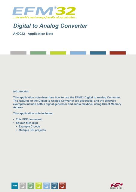
...the world's most energy friendly microcontrollers<br />
<strong>Digital</strong> <strong>to</strong> <strong>Analog</strong> <strong>Converter</strong><br />
<strong>AN0022</strong> - <strong>Application</strong> <strong>Note</strong><br />
Introduction<br />
This application note describes how <strong>to</strong> use the EFM32 <strong>Digital</strong> <strong>to</strong> <strong>Analog</strong> <strong>Converter</strong>.<br />
The features of the <strong>Digital</strong> <strong>to</strong> <strong>Analog</strong> <strong>Converter</strong> are described, and the software<br />
examples include both a signal genera<strong>to</strong>r and audio playback using Direct Memory<br />
Access.<br />
This application note includes:<br />
• This PDF document<br />
• Source files (zip)<br />
• Example C-code<br />
• Multiple IDE projects
1 <strong>Digital</strong> <strong>to</strong> <strong>Analog</strong> <strong>Converter</strong><br />
1.1 Introduction<br />
...the world's most energy friendly microcontrollers<br />
The EFM32 DAC is a 12 bit rail <strong>to</strong> rail <strong>Digital</strong> <strong>to</strong> <strong>Analog</strong> converter with either two single ended outputs,<br />
or one differential output. The maximum conversion rate is 500 ksamples/s at 12 bits resolution. One<br />
of the DAC's internal bandgap references or the VDD voltage can be selected as reference. The DAC<br />
may be used for a number of different applications such as sensor interfaces, voltage generation or<br />
sound/signal output.<br />
This application note shows general operation and usage of the DAC. In addition the sine genera<strong>to</strong>r<br />
mode is described and the different conversion modes are explained. The software examples include<br />
both an advanced signal genera<strong>to</strong>r and audio playback that both use DMA (Direct Memory Access) and<br />
the PRS (Peripheral Reflex System).<br />
1.2 Overview<br />
Figure 1.1. <strong>Digital</strong> <strong>to</strong> <strong>Analog</strong> <strong>Converter</strong> Overview<br />
CH0DATA<br />
Ch 0<br />
DACn_OUT0<br />
CH1DATA<br />
Ch 1<br />
DACn_OUT1<br />
1.25 V<br />
2.5 V<br />
VDD<br />
ADC<br />
REFSEL<br />
In Figure 1.1 (p. 2) , the two data registers and the reference selection register are shown in grey.<br />
The DAC has a single reference selection for both channels. The output can be routed <strong>to</strong> the ADC and<br />
output on a pin at the same time.<br />
2013-09-16 - an0022_Rev1.10 2 www.silabs.com
2 General Operation<br />
2.1 Clock Prescaling<br />
...the world's most energy friendly microcontrollers<br />
The DAC clock is supplied by a DAC-clock prescaler which divides the peripheral clock (HFPERCLK)<br />
by a fac<strong>to</strong>r of 2 n between 1 and 128. The resulting DAC_CLK is used by the converter core and the<br />
frequency is given by Equation 2.1 (p. 3) :<br />
Clock Prescaling<br />
f DAC_CLK = f HFPERCLK / 2 ^ PRESC (2.1)<br />
where f HFPERCLK is the HFPERCLK frequency. One conversion takes 2 DAC_CLK cycles and the<br />
DAC_CLK should not be set higher than 1 MHz. This is taken care of when using the emlib function<br />
for calculating the prescaler.<br />
Normally the PRESCALER runs continuously when either of the channels are enabled. When running<br />
with a prescaler setting higher than 0, there will be an unpredictable delay from the time the conversion<br />
was triggered <strong>to</strong> the time the actual conversion takes place. This is because the conversions is controlled<br />
by the prescaled clock and the conversion can arrive at any time during a prescaled clock (DAC_CLK)<br />
period. However, if the CH0PRESCRST bit in DACn_CTRL is set, the prescaler will be reset every time<br />
a conversion is triggered on channel 0. This leads <strong>to</strong> a predictable latency between channel 0 trigger<br />
and conversion.<br />
2.2 Output Selection<br />
The 2 single ended outputs of the DAC can either be used as two separate channels, or combined <strong>to</strong><br />
form one differential output channel by setting the DIFF bit in DACn_CTRL.<br />
2.2.1 Single Ended Mode<br />
When operating in single ended mode, the channel 0 output is on DACn_OUT0 and the channel 1 output<br />
is on DACn_OUT1. The output voltage can be calculated using Equation 2.2 (p. 3)<br />
Single Ended Output Voltage<br />
V OUT = V DACn_OUTx - V SS = V ref x CHxDATA/4096 (2.2)<br />
where CHxDATA is a 12-bit unsigned integer.<br />
2.2.2 Differential Mode<br />
When operating in differential mode, both DAC outputs are used for the differential voltage. The<br />
differential conversion uses DACn_CH0DATA as source. The positive output is on DACn_OUT1 and<br />
the negative output is on DACn_OUT0. Since the output can be negative, it is expected that the data is<br />
written in 2’s complement form with the MSB of the 12-bit value being the sign bit. The output voltage<br />
can be calculated using Equation 2.3 (p. 3) :<br />
Differential Output Voltage<br />
V OUT = V DACn_OUT1 - V DACn_OUT0 = V ref x CH0DATA/2048 (2.3)<br />
where CH0DATA is a 12-bit signed integer. The common mode voltage is V ref /2.<br />
2.3 Reference Selection<br />
Three internal voltage references are available and are selected by setting the REFSEL bits in<br />
DACn_CTRL:<br />
2013-09-16 - an0022_Rev1.10 3 www.silabs.com
...the world's most energy friendly microcontrollers<br />
• Internal 2.5V<br />
• Internal 1.25V<br />
• V DD<br />
The reference selection should only be changed while both channels are disabled. The references for<br />
the DAC need <strong>to</strong> be enabled for some time before they can be used. This is called the warm-up period,<br />
and starts when one of the channels is enabled. For a bandgap reference, this period is 5 DAC_CLK<br />
cycles while the V DD reference needs 1 DAC_CLK cycle. The DAC will time this period au<strong>to</strong>matically<br />
(given that the prescaler is set correctly) and delay any conversion triggers received during the warmup<br />
until the references have stabilized.<br />
The bias current of the bandgap reference and the DAC output buffer can be scaled by writing the<br />
BIASPROG and HALFBIAS bit fields of the DACn_BIASPROG register. To be sure the DAC has the<br />
characteristics stated in the datasheet within the specified frequency range, the default values for the<br />
bias currents should be used.<br />
2.4 Conversion Mode<br />
The DAC supports three different conversion modes, continuous, sample-hold and sample-off. By<br />
selecting sample-hold or sample-off mode the power consumption can be reduced compared <strong>to</strong><br />
continuous mode since the DAC is shut off between new samples or output refresh cycles.<br />
2.4.1 Continuous Mode<br />
In continuous mode the DAC channels will drive their outputs continuously with the data in the<br />
DACn_CHxDATA registers. This mode will maintain the output voltage and refresh is therefore not<br />
needed. Since the continuous mode makes the DAC convert constantly, this mode consumes the most<br />
power.<br />
2.4.2 Sample-Hold Mode<br />
In sample-hold mode, the DAC converts data on a triggered conversion and then holds the output at the<br />
converted voltage. When not converting between samples, the DAC core is turned off, which reduces<br />
the energy consumption. Because of holding element leakage, the output voltage will drift if the output<br />
is not refreshed by the DAC. The drift rate is specified in the datasheet.<br />
A refresh of the channel will happen when a new value is written <strong>to</strong> the DACn_CHxDATA register.<br />
Au<strong>to</strong>matic refresh can also be enabled by setting the bit REFREN in DACn_CHxCTRL. The refresh<br />
period can be selected by changing the REFRSEL value in the DACn_CTRL register. 4 different refresh<br />
periods can be selected, a longer period will be more energy efficient, while a shorter period gives less<br />
voltage drift.<br />
Since the refresh period is defined by a number of DAC clock cycles, the refresh interval will be<br />
dependent on the DAC clock speed.<br />
2.4.3 Sample-Off Mode<br />
In sample-off mode the DAC and the sample-hold element are turned completely off between samples,<br />
tristating the DAC output. This requires the DAC output voltage <strong>to</strong> be held externally. The references<br />
are also turned off between samples, which means that a new warm-up period is needed before each<br />
conversion. The DAC will time this period au<strong>to</strong>matically and delay any conversion triggers received<br />
during the warm- up until the references have stabilized.<br />
2.5 Conversion Start<br />
The DAC channel must be enabled before it can be used. When the channel is enabled, a conversion<br />
can be started by writing <strong>to</strong> the DACn_CHxDATA register. These data registers are also mapped in<strong>to</strong><br />
2013-09-16 - an0022_Rev1.10 4 www.silabs.com
...the world's most energy friendly microcontrollers<br />
a combined data register, DACn_COMBDATA, where the data values for both channels can be written<br />
simultaneously. Writing <strong>to</strong> this register will start a conversion on all enabled channels.<br />
If the PRSEN bit in DACn_CHxCTRL is set, a DAC conversion on channel x will not be started by data<br />
write, but when a positive one HFPERCLK cycle pulse is received on the PRS input selected by PRSSEL<br />
in DACn_CHxCTRL.<br />
The CH0DV and CH1DV bits in DACn_STATUS are set high when the corresponding channel contains<br />
data that has not yet been converted.<br />
2013-09-16 - an0022_Rev1.10 5 www.silabs.com
3 Advanced Features<br />
...the world's most energy friendly microcontrollers<br />
3.1 Sine Genera<strong>to</strong>r Mode<br />
The DAC contains an au<strong>to</strong>matic sine genera<strong>to</strong>r mode, which is enabled by setting the SINEMODE bit<br />
in the DACn_CTRL register. In this mode, the DAC data registers are overridden with conversion data<br />
taken from a hardware sine lookup table. The lookup table consist of 16 samples. When the OUTENPRS<br />
bit in DACn_CTRL is cleared, the sine genera<strong>to</strong>r will output the next sine-sample when a PRS conversion<br />
trigger pulse is received. This is illustrated in Figure 3.1 (p. 6) .<br />
Figure 3.1. Sine Genera<strong>to</strong>r Mode with PRS-triggered Samples<br />
One PRS HFCLK Pulse<br />
PRS pulse period changed<br />
CH0 PRS<br />
DACn_OUT0<br />
Sine Samples<br />
By having a timer supply the PRS pulses on compare or overflow the frequency of the sine wave can<br />
be accurately controlled.<br />
If the OUTENPRS bit is set, the PRS channels selected by PRSSEL in DACn_CH0CTRL and<br />
DACn_CH1CTRL switches on and off the sine wave (CH0 PRSSEL) and output driver (CH1 PRSSEL).<br />
The sine genera<strong>to</strong>r will now trigger new conversions by itself. If the channel 0 PRS line is low, a voltage<br />
of Vref/2 will be produced. When the line is high, the sine wave will be produced. The PRS line selected<br />
for channel 1 controls the output-driver which is tristated when the PRS line is low. This is illustrated<br />
in Figure 3.2 (p. 7) .<br />
The frequency when the OUTENPRS bit is set is given by Equation 3.1 (p. 6) :<br />
Sine Generation with OUTENPRS bit set<br />
f sine = f HFPERCLK / 32 x (PRESC + 1) (3.1)<br />
The sine wave will be output on channel 0. If the DIFF bit is set in DACn_CTRL, the sine wave will be<br />
output on both channels (if enabled), but inverted on the second channel (see Figure 3.2 (p. 7) ).<br />
<strong>Note</strong> that when OUTENPRS in DACn_CTRL is set, the sine output will be reset <strong>to</strong> 0 degrees when the<br />
PRS line selected by CH0PRSSEL is low.<br />
2013-09-16 - an0022_Rev1.10 6 www.silabs.com
Figure 3.2. Sine Generation with OUTENPRS bit set<br />
...the world's most energy friendly microcontrollers<br />
CH0 PRS<br />
CH1 PRS<br />
Vref<br />
DACn_OUT1<br />
Hi- Z<br />
Vref/ 2<br />
0<br />
Vref<br />
DACn_OUT0<br />
Hi- Z<br />
Vref/ 2<br />
0<br />
In Figure 3.2 (p. 7) , when the OUTENPRS bit in DACn_CH0CTRL is set, the PRS-lines selected<br />
by CH0PRSSEL and CH1PRSSEL enables the output driver and starts or s<strong>to</strong>ps the sine genera<strong>to</strong>r.<br />
3.2 Peripheral Reflex System and Interrupts<br />
Both DAC channels have separate interrupt flags (in DACn_IF) indicating that a conversion has finished<br />
on the channel and that new data can be written <strong>to</strong> the data registers. Setting one of these flags will result<br />
in a DAC interrupt request if the corresponding interrupt enable bit is set in DACn_IEN. All generated<br />
interrupt requests from the DAC will activate the same interrupt vec<strong>to</strong>r when enabled.<br />
The DAC has two PRS outputs which will carry a one cycle (HFPERCLK) high pulse when the<br />
corresponding channel has finished a conversion.<br />
3.3 Direct Memory Access<br />
In addition <strong>to</strong> the PRS output, the DAC sends out a DMA request when a conversion on a channel is<br />
complete. This request is cleared when the corresponding channel´s data register or the COMBDATA<br />
register is written.<br />
3.4 Calibration<br />
The DAC contains a calibration register, DACn_CAL, where calibration values for both offset and gain<br />
correction can be written. Offset calibration is done separately for each channel through the CHxOFFSET<br />
bitfields. Gain is calibrated in one common register field, GAIN.<br />
The calibration values are linked <strong>to</strong> the reference and when the reference is changed, the correct<br />
calibration values should be written <strong>to</strong> the calibration register. Gain and offset for the 1V25, 2V5 and<br />
VDD references are calibrated during production and the calibration values for these can be found in<br />
the Device Information page. The correct calibration values are loaded au<strong>to</strong>matically when using the<br />
emlib for configuring the DAC.<br />
The DAC can also be calibrated manually. Either the internal ADC or an external voltage meter can be<br />
used <strong>to</strong> measure the DAC output voltage. If the ADC is used, it should be calibrated first as described<br />
in the AN0021 - ADC application note. The procedure for calibrating the DAC is similar <strong>to</strong> the ADC<br />
calibration procedure.<br />
2013-09-16 - an0022_Rev1.10 7 www.silabs.com
...the world's most energy friendly microcontrollers<br />
• Offset is calibrated first by converting the value 0, and changing the calibration register until the output<br />
equals 0 V. The algorithm should take in<strong>to</strong> account that the offset might be far below 0, but the output<br />
will still be 0.<br />
• Gain should be calibrated after offset by converting the <strong>to</strong>p value: 2 12 -1 and adjusting the gain<br />
calibration register until the output almost equals the reference value (1-2 LSB's below) in order <strong>to</strong><br />
avoid overshoot.<br />
2013-09-16 - an0022_Rev1.10 8 www.silabs.com
4 Software Examples<br />
...the world's most energy friendly microcontrollers<br />
4.1 Programmable Voltage Source<br />
This example configures the DAC in continuous mode and converts a single value continuously. By<br />
entering EM1 the DAC operates independently. Since the DAC is operating in continuous mode, the<br />
output voltage will be stable even if the output is loaded. The fact that the DAC is continuously working<br />
will be reflected by the power consumption.<br />
4.2 Sample-Hold Mode with Au<strong>to</strong>matic Refresh<br />
This example basically does exactly the same thing as the first example, but now with the sample-hold<br />
mode which causes the DAC <strong>to</strong> be disabled between conversions. The internal output stage will hold<br />
the output value while the DAC is shut off for a number of cycles. The refresh rate which controls how<br />
often the DAC is woken up <strong>to</strong> refresh the holding element is adjustable.<br />
4.3 Sine Genera<strong>to</strong>r Mode with Timer<br />
This example demonstrates how <strong>to</strong> use a timer <strong>to</strong> send PRS-pulses which in turn triggers new DAC<br />
conversions. The DAC is configured in Sine Genera<strong>to</strong>r Mode. A sine wave with variable frequency is<br />
available on the DAC output pins. The frequency is adjusted by changing the timer overflow value. After<br />
configuration, energymode 1 is entered <strong>to</strong> save power.<br />
4.4 Signal Genera<strong>to</strong>r<br />
The Signal Genera<strong>to</strong>r shows how TIMER0, PRS, DMA and the DAC can be used in cooperation <strong>to</strong><br />
generate different glitch-free waveforms from tables in flash memory. The example code only works on<br />
the DK because it uses the joystick and the but<strong>to</strong>ns <strong>to</strong> change the signal parameters. It can be easily<br />
modified <strong>to</strong> work on other platforms than the DK, but without the user interface.<br />
The DMA is configured in ping pong mode <strong>to</strong> be able <strong>to</strong> supply new data <strong>to</strong> the DAC continuously without<br />
software intervention between memory-buffer changes. New DAC samples are triggered by a PRS-pulse<br />
from the Timer. The DAC sends DMA-requests immediately after a conversion <strong>to</strong> have a new data value<br />
ready for the next PRS-pulse.<br />
The signal genera<strong>to</strong>r can operate in both fixed and variable sampling frequency mode. In the fixed<br />
sampling frequency mode, the amount of samples used for each period of the signal is adjusted <strong>to</strong><br />
match the desired signal frequency. In variable sampling frequency mode the time between PRS-pulses<br />
is adjusted and each signal period is made up of a fixed number of samples. Because of the limited<br />
amount of look up table samples available for each cycle, the frequency in fixed sampling frequency<br />
mode can not be adjusted as accurately as in the variable sampling frequency case. The fixed sampling<br />
frequency case is illustrated in Figure 4.1 (p. 10) , while an example of variable sampling frequency<br />
can be seen in Figure 3.1 (p. 6) .<br />
2013-09-16 - an0022_Rev1.10 9 www.silabs.com
...the world's most energy friendly microcontrollers<br />
Figure 4.1. Fixed Sampling Frequency<br />
Fixed Sampling Intervals<br />
CH0 PRS<br />
DACn_OUT0<br />
Sine Samples<br />
Double Number of<br />
Samples<br />
The but<strong>to</strong>ns and joystick on the DK are used <strong>to</strong> configure offset, amplitude, frequency, signal type and<br />
<strong>to</strong> switch between fixed/variable sampling frequency. After pushing the AEM but<strong>to</strong>n on the DK <strong>to</strong> enable<br />
the switches and joystick for the application, the user can select different waveforms by pushing up or<br />
down on the joystick. Frequency is adjusted by pushing left or right, and amplitude/offset is adjusted<br />
with the but<strong>to</strong>ns. By pressing the center but<strong>to</strong>n of the joystick, the signal genera<strong>to</strong>r switches between<br />
fixed and variable sampling frequency.<br />
The code flow and operation is outlined below:<br />
• The main function enables and configures the DAC, Timer, PRS and DMA. It then fills the two ping<br />
pong memory buffers with the first waveform data. Then it enters a while loop that just enters EM1<br />
after each interrupt. The actual handling of the memory buffers are done in the DMA-finished interrupt<br />
routine.<br />
• A new sample is converted by the DAC on each new PRS-pulse from the Timer. The DAC then<br />
requests new data from the DMA, which immediately after a conversion fills the DAC data register<br />
with a new sample from the currently active buffer.<br />
• When the DMA has iterated through the currently active buffer it immediately switches <strong>to</strong> the alternate<br />
buffer which is ready with new samples.<br />
• The switch <strong>to</strong> the new buffer also triggers an interrupt. The interrupt routine reads user input from<br />
the but<strong>to</strong>ns and joystick and changes the signal parameters if new input is received. It then iterates<br />
through and fills the buffer that was just finished with new sample data. The sample data are calculated<br />
based on the correct waveform table and the current frequency/amplitude/offset settings. The last task<br />
done by the interrupt is <strong>to</strong> reactivate the newly filled buffer for the DMA.<br />
The ping pong operation of the DMA is illustrated in Figure 4.2 (p. 11) .<br />
2013-09-16 - an0022_Rev1.10 10 www.silabs.com
...the world's most energy friendly microcontrollers<br />
Figure 4.2. Ping Pong Operation of DMA<br />
DAC requests <strong>to</strong> DMA<br />
Request<br />
Request<br />
Request<br />
Request<br />
Primary Buffer<br />
Sample 1<br />
Sample 2<br />
Sample 3<br />
Sample 4<br />
DMA memory pointer<br />
incremented for each<br />
request<br />
Request<br />
Sample n<br />
dma_done_interrupt<br />
DMA controller switches <strong>to</strong><br />
next buffer immediately<br />
DAC requests <strong>to</strong> DMA<br />
Request<br />
Request<br />
Request<br />
Request<br />
Alternate Buffer<br />
Sample 1<br />
Sample 2<br />
Sample 3<br />
Sample 4<br />
DMA memory pointer<br />
incremented for each<br />
request<br />
Request<br />
Sample n<br />
dma_done_interrupt<br />
4.5 Audio Playback<br />
This example requires the DK with a FAT formatted microSD card that supports SPI communication. By<br />
default it looks for a file named "soundfile.wav" and plays this file at the sampling frequency specified in<br />
the wav-file. Both stereo and mono files are supported, but only 16 bit sample size. The example uses<br />
the same ping pong DMA transfer scheme as the signal genera<strong>to</strong>r, but the sample data are fetched<br />
from the microSD-card instead of tables in flash. The code flow is very similar, only adding microSDcard<br />
access and excluding user input.<br />
The audio out line on the DK consists of a line driver amplifier with a filter which works best at or above<br />
44.1kHz sampling frequency because of a designed cut-off frequency around 20kHz. There is no volume<br />
control therefore you should not connect headphones directly <strong>to</strong> the output. Computer speakers with<br />
volume control are a better choice.<br />
4.6 DAC Calibration<br />
If the EFM32 is operated at high/low temperatures it could be necessary <strong>to</strong> recalibrate the DAC <strong>to</strong> obtain<br />
the specified performance. The calibration values that are s<strong>to</strong>red in the Device Information Page are<br />
valid for room temperature, but a significant change in temperature could decrease the DAC accuracy.<br />
A calibration routine example that recalibrates the DAC using the internal ADC is supplied with this<br />
application note.<br />
2013-09-16 - an0022_Rev1.10 11 www.silabs.com
...the world's most energy friendly microcontrollers<br />
DAC calibration is performed in two steps, first the offset is calibrated by adjusting the DAC calibration<br />
register until a digital value of 0 gives 0 V on the output. The second step is gain calibration, now the<br />
calibration register is adjusted so that the maximum digital value gives an output voltage that is close<br />
or equal <strong>to</strong> the reference voltage selected. The calibration routine uses the ADC <strong>to</strong> calibrate the DAC.<br />
The internal connection between the DAC and the ADC is used, so no external connection between the<br />
ADC and DAC is necessary.<br />
Since the ADC is used <strong>to</strong> calibrate the DAC, it is important that the ADC is calibrated before it is used<br />
<strong>to</strong> calibrate the DAC. This calibration is included in the example, but it requires an external reference<br />
voltage <strong>to</strong> be applied <strong>to</strong> ADC input channel 4 (all channels can be used).<br />
2013-09-16 - an0022_Rev1.10 12 www.silabs.com
5 Revision His<strong>to</strong>ry<br />
...the world's most energy friendly microcontrollers<br />
5.1 Revision 1.10<br />
2013-09-03<br />
New cover layout<br />
5.2 Revision 1.09<br />
2013-05-08<br />
Added software projects for ARM-GCC and A<strong>to</strong>llic TrueStudio.<br />
Adapted signal genera<strong>to</strong>r software project <strong>to</strong> different user input on gecko vs. giant gecko development<br />
kits.<br />
5.3 Revision 1.08<br />
2012-11-12<br />
Adapted software projects <strong>to</strong> new kit-driver and bsp structure.<br />
5.4 Revision 1.07<br />
2012-08-14<br />
Added projects for Tiny and Giant Gecko STKs.<br />
Updated file paths for fatfs<br />
5.5 Revision 1.06<br />
2012-04-20<br />
Adapted software projects <strong>to</strong> new peripheral library naming and CMSIS_V3.<br />
5.6 Revision 1.05<br />
2011-11-17<br />
Updated IDE project paths with new kits direc<strong>to</strong>ry.<br />
5.7 Revision 1.04<br />
2011-05-18<br />
Updated projects <strong>to</strong> align with new bsp version.<br />
5.8 Revision 1.03<br />
2011-05-16<br />
Code update, low pass filter removed from DAC initialization structure.<br />
2013-09-16 - an0022_Rev1.10 13 www.silabs.com
...the world's most energy friendly microcontrollers<br />
5.9 Revision 1.02<br />
2011-04-07<br />
Changed error in DMA_ActivatePingPong() function calling<br />
5.10 Revision 1.01<br />
2010-11-16<br />
Updated chip init function <strong>to</strong> newest efm32lib version.<br />
Updated register defines in code <strong>to</strong> match newest efm32lib release.<br />
5.11 Revision 1.00<br />
2010-11-08<br />
Initial revision.<br />
2013-09-16 - an0022_Rev1.10 14 www.silabs.com
A Disclaimer and Trademarks<br />
A.1 Disclaimer<br />
...the world's most energy friendly microcontrollers<br />
<strong>Silicon</strong> Labora<strong>to</strong>ries intends <strong>to</strong> provide cus<strong>to</strong>mers with the latest, accurate, and in-depth documentation<br />
of all peripherals and modules available for system and software implementers using or intending <strong>to</strong> use<br />
the <strong>Silicon</strong> Labora<strong>to</strong>ries products. Characterization data, available modules and peripherals, memory<br />
sizes and memory addresses refer <strong>to</strong> each specific device, and "Typical" parameters provided can and<br />
do vary in different applications. <strong>Application</strong> examples described herein are for illustrative purposes<br />
only. <strong>Silicon</strong> Labora<strong>to</strong>ries reserves the right <strong>to</strong> make changes without further notice and limitation <strong>to</strong><br />
product information, specifications, and descriptions herein, and does not give warranties as <strong>to</strong> the<br />
accuracy or completeness of the included information. <strong>Silicon</strong> Labora<strong>to</strong>ries shall have no liability for<br />
the consequences of use of the information supplied herein. This document does not imply or express<br />
copyright licenses granted hereunder <strong>to</strong> design or fabricate any integrated circuits. The products must<br />
not be used within any Life Support System without the specific written consent of <strong>Silicon</strong> Labora<strong>to</strong>ries.<br />
A "Life Support System" is any product or system intended <strong>to</strong> support or sustain life and/or health, which,<br />
if it fails, can be reasonably expected <strong>to</strong> result in significant personal injury or death. <strong>Silicon</strong> Labora<strong>to</strong>ries<br />
products are generally not intended for military applications. <strong>Silicon</strong> Labora<strong>to</strong>ries products shall under no<br />
circumstances be used in weapons of mass destruction including (but not limited <strong>to</strong>) nuclear, biological<br />
or chemical weapons, or missiles capable of delivering such weapons.<br />
A.2 Trademark Information<br />
<strong>Silicon</strong> Labora<strong>to</strong>ries Inc., <strong>Silicon</strong> Labora<strong>to</strong>ries, the <strong>Silicon</strong> <strong>Labs</strong> logo, Energy Micro, EFM, EFM32, EFR,<br />
logo and combinations thereof, and others are the registered trademarks or trademarks of <strong>Silicon</strong><br />
Labora<strong>to</strong>ries Inc. ARM, CORTEX, Cortex-M3 and THUMB are trademarks or registered trademarks<br />
of ARM Holdings. Keil is a registered trademark of ARM Limited. All other products or brand names<br />
mentioned herein are trademarks of their respective holders.<br />
2013-09-16 - an0022_Rev1.10 15 www.silabs.com
B Contact Information<br />
...the world's most energy friendly microcontrollers<br />
<strong>Silicon</strong> Labora<strong>to</strong>ries Inc.<br />
400 West Cesar Chavez<br />
Austin, TX 78701<br />
Please visit the <strong>Silicon</strong> <strong>Labs</strong> Technical Support web page:<br />
http://www.silabs.com/support/pages/contacttechnicalsupport.aspx<br />
and register <strong>to</strong> submit a technical support request.<br />
2013-09-16 - an0022_Rev1.10 16 www.silabs.com
...the world's most energy friendly microcontrollers<br />
Table of Contents<br />
1. <strong>Digital</strong> <strong>to</strong> <strong>Analog</strong> <strong>Converter</strong> ......................................................................................................................... 2<br />
1.1. Introduction .................................................................................................................................... 2<br />
1.2. Overview ....................................................................................................................................... 2<br />
2. General Operation ..................................................................................................................................... 3<br />
2.1. Clock Prescaling ............................................................................................................................. 3<br />
2.2. Output Selection ............................................................................................................................. 3<br />
2.3. Reference Selection ........................................................................................................................ 3<br />
2.4. Conversion Mode ............................................................................................................................ 4<br />
2.5. Conversion Start ............................................................................................................................. 4<br />
3. Advanced Features .................................................................................................................................... 6<br />
3.1. Sine Genera<strong>to</strong>r Mode ...................................................................................................................... 6<br />
3.2. Peripheral Reflex System and Interrupts ............................................................................................. 7<br />
3.3. Direct Memory Access ..................................................................................................................... 7<br />
3.4. Calibration ..................................................................................................................................... 7<br />
4. Software Examples .................................................................................................................................... 9<br />
4.1. Programmable Voltage Source .......................................................................................................... 9<br />
4.2. Sample-Hold Mode with Au<strong>to</strong>matic Refresh ......................................................................................... 9<br />
4.3. Sine Genera<strong>to</strong>r Mode with Timer ....................................................................................................... 9<br />
4.4. Signal Genera<strong>to</strong>r ............................................................................................................................ 9<br />
4.5. Audio Playback ............................................................................................................................. 11<br />
4.6. DAC Calibration ............................................................................................................................ 11<br />
5. Revision His<strong>to</strong>ry ...................................................................................................................................... 13<br />
5.1. Revision 1.10 ............................................................................................................................... 13<br />
5.2. Revision 1.09 ............................................................................................................................... 13<br />
5.3. Revision 1.08 ............................................................................................................................... 13<br />
5.4. Revision 1.07 ............................................................................................................................... 13<br />
5.5. Revision 1.06 ............................................................................................................................... 13<br />
5.6. Revision 1.05 ............................................................................................................................... 13<br />
5.7. Revision 1.04 ............................................................................................................................... 13<br />
5.8. Revision 1.03 ............................................................................................................................... 13<br />
5.9. Revision 1.02 ............................................................................................................................... 14<br />
5.10. Revision 1.01 .............................................................................................................................. 14<br />
5.11. Revision 1.00 .............................................................................................................................. 14<br />
A. Disclaimer and Trademarks ....................................................................................................................... 15<br />
A.1. Disclaimer ................................................................................................................................... 15<br />
A.2. Trademark Information ................................................................................................................... 15<br />
B. Contact Information ................................................................................................................................. 16<br />
B.1. ................................................................................................................................................. 16<br />
2013-09-16 - an0022_Rev1.10 17 www.silabs.com
...the world's most energy friendly microcontrollers<br />
List of Figures<br />
1.1. <strong>Digital</strong> <strong>to</strong> <strong>Analog</strong> <strong>Converter</strong> Overview ......................................................................................................... 2<br />
3.1. Sine Genera<strong>to</strong>r Mode with PRS-triggered Samples ....................................................................................... 6<br />
3.2. Sine Generation with OUTENPRS bit set .................................................................................................... 7<br />
4.1. Fixed Sampling Frequency ...................................................................................................................... 10<br />
4.2. Ping Pong Operation of DMA .................................................................................................................. 11<br />
2013-09-16 - an0022_Rev1.10 18 www.silabs.com
...the world's most energy friendly microcontrollers<br />
List of Equations<br />
2.1. Clock Prescaling ..................................................................................................................................... 3<br />
2.2. Single Ended Output Voltage .................................................................................................................... 3<br />
2.3. Differential Output Voltage ........................................................................................................................ 3<br />
3.1. Sine Generation with OUTENPRS bit set .................................................................................................... 6<br />
2013-09-16 - an0022_Rev1.10 19 www.silabs.com