

Xcell on the Web - Xilinx
Xcell on the Web - Xilinx
Xcell on the Web - Xilinx

You also want an ePaper? Increase the reach of your titles
YUMPU automatically turns print PDFs into web optimized ePapers that Google loves.
20<br />
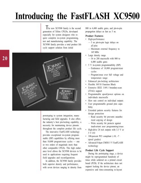
Introducing <strong>the</strong> FastFLASH XC9500<br />
The new XC9500 family is <strong>the</strong> sec<strong>on</strong>d<br />
generati<strong>on</strong> of <strong>Xilinx</strong> CPLDs, developed<br />
especially for system designers who require<br />
complete in-system programming,<br />
test and manufacturing capability. The<br />
XC9500 family provides a total product life<br />
cycle support soluti<strong>on</strong> from initial<br />
prototyping to system integrati<strong>on</strong>, manufacturing<br />
and field upgrades. It also offers<br />
<strong>the</strong> industry’s best pin-locking capability, a<br />
necessity for maintaining device pinouts<br />
throughout <strong>the</strong> complete product life cycle.<br />
The innovative FastFLASH technology<br />
provides excepti<strong>on</strong>al in-system programmable<br />
(ISP) capabilities by offering more<br />
than 10,000 program/erase cycles — <strong>on</strong>e<br />
or two orders of magnitude more than<br />
o<strong>the</strong>r comparable CPLDs. This high endurance<br />
level allows <strong>the</strong> XC9500 devices to be<br />
used in applicati<strong>on</strong>s requiring frequent<br />
field upgrades and rec<strong>on</strong>figurati<strong>on</strong>s.<br />
In additi<strong>on</strong>, <strong>the</strong> XC9500 family provides<br />
both superior density and performance,<br />
with seven devices ranging in density from<br />
800 to 6,400 usable gates, and pin-to-pin<br />
propagati<strong>on</strong> delays as fast as 5 ns.<br />
Product Features<br />
• High-performance<br />
— 5 ns pin-to-pin logic delays <strong>on</strong><br />
all pins<br />
— Maximum external frequency to<br />
145 MHz<br />
• Large density range<br />
— 36 to 288 macrocells with 800 to<br />
6,400 usable gates<br />
• 5 V in-system programmability (ISP)<br />
— Endurance of 10,000 program/erase<br />
cycles<br />
— Program/erase over full voltage and<br />
temperature range<br />
• Enhanced pin-locking architecture<br />
• Flexible 36V18 Functi<strong>on</strong> Block<br />
• Extensive IEEE 1149.1 boundary-scan<br />
(JTAG) support<br />
• Programmable speed/power opti<strong>on</strong>s <strong>on</strong><br />
individuals macrocells<br />
• Slew rate c<strong>on</strong>trol <strong>on</strong> individual outputs<br />
• User programmable ground pins capability<br />
• Extended pattern security features for<br />
design protecti<strong>on</strong><br />
— Read security bit prevents unauthorized<br />
copying of design<br />
— Write security bit protects against<br />
inadvertent user programming/erase<br />
• High-drive 24 mA outputs with 3.3 V or<br />
5 V I/O<br />
• 100-percent PCI compliant (-10, -7<br />
speed grades)<br />
• Advanced 0.6µm CMOS 5 V FastFLASH<br />
technology<br />
Product Life Cycle Support<br />
During <strong>the</strong> prototyping stage, a device<br />
might be reprogrammed hundreds of<br />
times while soldered <strong>on</strong> a printed circuit<br />
board (PCB). If <strong>the</strong> architecture does not<br />
support locking <strong>the</strong> device pinout, an<br />
expensive and time-c<strong>on</strong>suming re-layout


