

Xcell on the Web - Xilinx
Xcell on the Web - Xilinx
Xcell on the Web - Xilinx

Create successful ePaper yourself
Turn your PDF publications into a flip-book with our unique Google optimized e-Paper software.
30<br />
Write<br />
Operati<strong>on</strong>s<br />
Synchr<strong>on</strong>ous RAM Timing in <strong>the</strong><br />
The XC4000E FPGA’s synchr<strong>on</strong>ous<br />
memory mode simplifies <strong>the</strong> timing of <strong>the</strong><br />
memory interface and c<strong>on</strong>trbutes to increased<br />
utilizati<strong>on</strong> and performance (as<br />
compared to asynchr<strong>on</strong>ous timing<br />
schemes). With proper attenti<strong>on</strong> to address<br />
routing delays, synchr<strong>on</strong>ous RAMs<br />
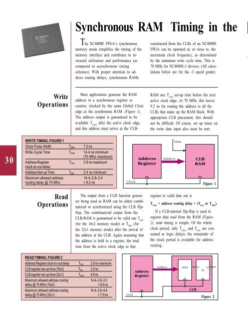
Most applicati<strong>on</strong>s generate <strong>the</strong> RAM<br />
address in a synchr<strong>on</strong>ous register or<br />
counter, clocked by <strong>the</strong> same Global Clock<br />
edge as <strong>the</strong> synchr<strong>on</strong>ous RAM (Figure 1).<br />
The address output is guaranteed to be<br />
available T CKO after <strong>the</strong> active clock edge,<br />
and this address must arrive at <strong>the</strong> CLB-<br />
c<strong>on</strong>structed from <strong>the</strong> CLBs of an XC4000E<br />
FPGA can be operated at, or close to, <strong>the</strong><br />
maximum clock frequency, as determined<br />
by <strong>the</strong> minimum write cycle time. This is<br />
70 MHz for XC4000E-3 devices. (All calculati<strong>on</strong>s<br />
below are for <strong>the</strong> -3 speed grade).<br />
RAM <strong>on</strong>e T ASS set-up time before <strong>the</strong> next<br />
active clock edge. At 70 MHz, this leaves<br />
9.2 ns for routing <strong>the</strong> address to all <strong>the</strong><br />
CLBs that make up <strong>the</strong> RAM block. With<br />
appropriate CLB placement, this should<br />
not be difficult. Of course, set up times <strong>on</strong><br />
<strong>the</strong> write data input also must be met.<br />
WRITE TIMING, FIGURE 1<br />
Clock Pulse Width T WPS 7.2 ns<br />
Write Cycle Time TWCS 14.4 ns minimum<br />
(70 MHz maximum)<br />
Address Register TCKO 2.8 ns maximum<br />
clock-to-out delay<br />
Address Set-up Time TASS 2.4 ns minimum<br />
Maximum allowed address 14.4–2.8–2.4<br />
routing delay @ 70 MHz = 9.2 ns Figure 1<br />
Read<br />
Operati<strong>on</strong>s<br />
The output from a CLB functi<strong>on</strong> generator<br />
being used as RAM can be ei<strong>the</strong>r combinatorial<br />
or synchr<strong>on</strong>ized using <strong>the</strong> CLB flipflop.<br />
The combinatorial output from <strong>the</strong><br />
CLB-RAM is guaranteed to be valid <strong>on</strong>e T ILO<br />
(for <strong>the</strong> 16x2 memory mode) or T IHO (for<br />
<strong>the</strong> 32x1 memory mode) after <strong>the</strong> arrival of<br />
<strong>the</strong> address at <strong>the</strong> CLB. Again assuming that<br />
<strong>the</strong> address is held in a register, <strong>the</strong> total<br />
time from <strong>the</strong> active clock edge at that<br />
READ TIMING, FIGURE 2<br />
Address Register clock-to-out delay TCKO 2.8 ns maximum<br />
CLB register set-up time (16x2) TICK 3.0 ns<br />
CLB register set-up time (32x1) TIHCK 4.6 ns<br />
Maximum allowed address routing 14.4–2.8–3.0<br />
delay @ 70 MHz (16x2) = 8.6 ns<br />
Maximum allowed address routing 14.4–2.8–4.6<br />
delay @ 70 MHz (32x1) = 7.0 ns<br />
register to valid data out is<br />
T CKO + address routing delay + (T ILO or T IHO ).<br />
If a CLB-internal flip-flop is used to<br />
register data read from <strong>the</strong> RAM (Figure<br />
2), read timing is simple. Of <strong>the</strong> whole<br />
clock period, <strong>on</strong>ly T CKO and T ICK are c<strong>on</strong>sumed<br />
as logic delays; <strong>the</strong> remainder of<br />
<strong>the</strong> clock period is available for address<br />
routing.<br />
Figure 2


