

Xcell on the Web - Xilinx
Xcell on the Web - Xilinx
Xcell on the Web - Xilinx

You also want an ePaper? Increase the reach of your titles
YUMPU automatically turns print PDFs into web optimized ePapers that Google loves.
34<br />
LOW LOW<br />
POWER POWER<br />
Minimizing Power C<strong>on</strong>sumpti<strong>on</strong><br />
in FPGA Designs<br />
In general, <strong>the</strong> CMOS technology used<br />
to produce FPGAs is a low-power technology.<br />
Virtually all power c<strong>on</strong>sumpti<strong>on</strong> results<br />
from <strong>the</strong> dynamic charging and discharging<br />
of internal capacitive nodes and<br />
capacitive loads <strong>on</strong> <strong>the</strong> device outputs.<br />
Here are some techniques that can be<br />
used to minimize power c<strong>on</strong>sumpti<strong>on</strong> in<br />
an FPGA design:<br />
• Chip outputs dissipate a lot of power.<br />
Use as few as possible, and have <strong>the</strong>m<br />
switch as infrequently as possible.<br />
Although <strong>the</strong>re is no need to three-state<br />
outputs unnecessarily, d<strong>on</strong>’t allow an<br />
output to change c<strong>on</strong>tinuously if <strong>the</strong><br />
external circuitry is ignoring <strong>the</strong> data.<br />
• Similarly, d<strong>on</strong>’t allow internal FPGA<br />
nodes to toggle unnecessarily. Clock<br />
enable functi<strong>on</strong>s <strong>on</strong> flip-flops often can<br />
be used to “turn off” inactive porti<strong>on</strong>s<br />
of a synchr<strong>on</strong>ous circuit.<br />
• Use APR or PPR (or even XDE) to maximize<br />
<strong>the</strong> performance of <strong>the</strong> design,<br />
even if <strong>the</strong> resulting performance is far<br />
in excess of requirements. Power dissi-<br />
User-Defined Schmitt Triggers<br />
pati<strong>on</strong> is proporti<strong>on</strong>al to capacitance,<br />
and routing capacitance is <strong>the</strong> main<br />
cause of low performance. Circuits that<br />
are able to run faster can do so because<br />
of lower routing capacitance. C<strong>on</strong>sequently,<br />
<strong>the</strong>y dissipate less power at<br />
any given clock frequency.<br />
• For XC3000A/XC3100A designs, use<br />
ACLK for global clocking, and floorplan<br />
to minimize <strong>the</strong> number of vertical<br />
clock segments used. This minimizes<br />
<strong>the</strong> power associated with clock<br />
distributi<strong>on</strong>.<br />
For very power-sensitive applicati<strong>on</strong>s,<br />
power c<strong>on</strong>sumpti<strong>on</strong> can be dramatically<br />
reduced by using <strong>the</strong> 3.3 V Zero+ XC2000L<br />
and XC3000L FPGA families. These devices<br />
were designed to provide very low quiescent<br />
current c<strong>on</strong>sumpti<strong>on</strong>, and c<strong>on</strong>sume<br />
less than half <strong>the</strong> dynamic power of <strong>the</strong>ir<br />
5 V counterparts. Also, remember that <strong>the</strong><br />
XC2000 and XC3000 FPGAs feature a<br />
power-down mode, wherein <strong>the</strong> FPGA’s<br />
c<strong>on</strong>figurati<strong>on</strong> is preserved, but all o<strong>the</strong>r<br />
circuitry is powered down. ◆<br />
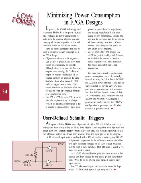
All inputs to <strong>Xilinx</strong> FPGAs have a hysteresis of 100 to 200 mV. It helps avoid noise<br />
propagati<strong>on</strong> from slowly rising or falling input signals. Users requiring more hysteresis can<br />
design <strong>the</strong>ir own Schmitt trigger circuits easily with <strong>on</strong>ly two resistors. However, it uses<br />
<strong>on</strong>e additi<strong>on</strong>al output pin, driven (n<strong>on</strong>-inverted) from <strong>the</strong> input pin, as in <strong>the</strong> diagram.<br />
A 10 kΩ serial input resistor combined with a 100 kΩ feedback resistor gives 500 mV<br />
of hysteresis. (Hysteresis is <strong>the</strong> difference between <strong>the</strong> effective<br />
input threshold voltages <strong>on</strong> <strong>the</strong> Low-to-High transiti<strong>on</strong><br />
and <strong>the</strong> High-to-Low transiti<strong>on</strong>. That difference is equal to V CC<br />
times <strong>the</strong> resistor ratio.)<br />
A 1 kΩ/10 kΩ combinati<strong>on</strong> gives <strong>the</strong> same hysteresis, but<br />
reduces <strong>the</strong> delay caused by <strong>the</strong> pin-to-ground capacitance<br />
from 100 ns to 10 ns. On <strong>the</strong> o<strong>the</strong>r hand, it requires more<br />
input current.<br />
For TTL-threshold inputs, <strong>the</strong> hysteresis should be kept<br />
below 1 V; for CMOS inputs, it can be up to 2 V. ◆


