Deposition of PZT thin films with - Advanced Materials Letters
Deposition of PZT thin films with - Advanced Materials Letters
Deposition of PZT thin films with - Advanced Materials Letters

You also want an ePaper? Increase the reach of your titles
YUMPU automatically turns print PDFs into web optimized ePapers that Google loves.
Research Article Adv. Mat. Lett. 2012, 3(2), 102-106 ADVANCED MATERIALS <strong>Letters</strong><br />
Introduction<br />
Lead zirconium titanate (<strong>PZT</strong>) <strong>thin</strong> <strong>films</strong> <strong>with</strong> the<br />
morphotropic phase boundary (MPB) composition is<br />
extensively used for Micro Electro Mechanical System<br />
(MEMS) applications due to high piezo characteristics<br />
<strong>of</strong>fered by them. For MEMS applications, the in-plane<br />
transverse piezo coefficient, e31 * is the most important<br />
parameter to be considered [1, 2]. The factors which<br />
influence e31 * are film thickness, film texture and<br />
compositional gradient across the film thickness [3, 4]. In<br />
microactuators, <strong>PZT</strong> <strong>films</strong> are typically 0.5-2.0 m in<br />
thickness. Thicker <strong>films</strong> are prone to have higher porosities<br />
and therefore lower dielectric breakdown strength. In <strong>thin</strong><br />
<strong>films</strong> the piezoelectric characteristics are significantly<br />
influenced by the contribution from domain wall movement<br />
[5, 6]. However, there is considerable scatter in data in the<br />
literature <strong>with</strong> respect to this extrinsic contribution to<br />
piezoelectric strain. It has been recently shown that <strong>PZT</strong><br />
<strong>thin</strong> <strong>films</strong> <strong>with</strong> MPB composition having {110}-preferred<br />
orientation exhibited high values <strong>of</strong> e31 * [7]. It is therefore<br />
<strong>of</strong> interest to compare the extent <strong>of</strong> extrinsic contributions<br />
to e31 * in textured <strong>thin</strong> <strong>films</strong> <strong>of</strong> <strong>PZT</strong> having MPB<br />
compositions. For MEMS applications like microbending<br />
actuators, high frequency filters, micropumps and pressure<br />
sensors, development <strong>of</strong> dense, crack-free piezoelectric<br />
<strong>films</strong> integrated on silicon substrates is essential [8, 9]. Of<br />
the various methods employed to deposit <strong>PZT</strong> <strong>thin</strong> <strong>films</strong>,<br />
chemical-solution deposition (CSD) <strong>of</strong>fers several<br />
advantages such as precise stoichiometry, lower processing<br />
temperatures and economy. Therefore, in the present study,<br />
we report fabrication <strong>of</strong> <strong>PZT</strong> <strong>thin</strong> <strong>films</strong> by CSD method and<br />
study the influence <strong>of</strong> preferred crystallographic orientation<br />
on e31 *<br />
Experimental<br />
Highly stable precursor solution <strong>of</strong> <strong>PZT</strong> was synthesized by<br />
a hybrid Metallo-Organic Decomposition (MOD) and solgel<br />
process adapting the procedure as discussed in our<br />
earlier work [10, 11]. The reactants, lead acetate (Merck,<br />
India) and zirconium acetyl acetone (Merck, India) were<br />
refluxed in 2-ethyl hexanoic acid (Sigma Aldrich, India).<br />
The substituted acetic acid and the excess 2- ethylhexanoic<br />
acid were removed through distillation and the brownish<br />
residue was dissolved in isopropyl alcohol containing<br />
titanium isopropoxide (Sigma Aldrich, India) in the<br />
presence <strong>of</strong> chelating agent diethanolamine (Sigma<br />
Aldrich, India) to yield a stable precursor solution. The<br />
solution was spin coated on to platinised silicon substrate<br />
[(111)Pt/Ti/SiO2/Si; Inostek, Korea], dried at 110 0 C for<br />
10min and then annealed at 650 0 C for 20 min after<br />
subjecting to an intermediate soaking for 10 min at 400 0 C.<br />
The coating and thermal treatment cycles were repeated to<br />
get {111}-oriented <strong>films</strong> <strong>of</strong> thickness 2.0 m. Before the<br />
deposition <strong>of</strong> <strong>PZT</strong> <strong>thin</strong> film, SrTiO3 (ST) layer having<br />
50nm thickness was used as the seeding layer. Different<br />
buffer layers like TiO2, and PbTiO3 were employed to get<br />
{001}, and {110}-preferred orientations respectively [12,<br />
13]. When TiO2 layer was used, SrTiO3 layer as described<br />
above was coated over it. The crystallographic orientation<br />
and phase <strong>of</strong> these deposited <strong>films</strong> were determined using<br />
x- ray diffractometer (XRD; Model: D55005, Bruker,<br />
Germany). Gold top electrodes (dia. ~0.35mm) were<br />
deposited by vacuum evaporation using a vacuum coater<br />
(Model: 12A4D, Hind High Vacuum, India). Dielectric and<br />
ferroelectric characteristics were determined using an<br />
Impedance analyzer (Model: 4294A, Agilent Technologies,<br />
USA) and Piezoelectric evaluation system (Model: TF<br />
Analyser 2000, aixACCT, Germany) respectively. Fatigue<br />
was studied using the piezoelectric evaluation system. For<br />
the measurement <strong>of</strong> the piezoelectric properties, rectangular<br />
specimens <strong>of</strong> dimensions (5.5 x 1.5) mm 2 were diced out<br />
from the substrates. The transverse piezoelectric properties<br />
<strong>of</strong> the <strong>PZT</strong> <strong>thin</strong> <strong>films</strong> were evaluated using unimorph<br />
cantilevers <strong>of</strong> <strong>PZT</strong>/Pt/Ti/SiO2/Si. The details <strong>of</strong> the<br />
measurements have been described in the previous reports<br />
[14, 15]. Application <strong>of</strong> sine wave voltage between upper<br />
and bottom electrodes generates the deflection by the<br />
transverse inverse piezoelectric effect, and the tip<br />
displacement was measured using a laser Doppler<br />
vibrometer (Model: AT-3500, Graphtec, Japan) and a laser<br />
interferometer (Model: AT-1100, Graphtec, Japan).<br />
Microstructural analysis <strong>of</strong> the film was recorded using a<br />
High Resolution Scanning Electron Microscope (HRSEM,<br />
Model FEI Quanta FEG 200, USA). Compositional<br />
analysis <strong>of</strong> <strong>thin</strong> <strong>films</strong> was carried out by energy dispersive<br />
analysis <strong>of</strong> x-rays (EDX) equipped <strong>with</strong> scanning electron<br />
microscope (Model: Genesis Apex 2, Ametek, Japan).<br />
Results and discussion<br />
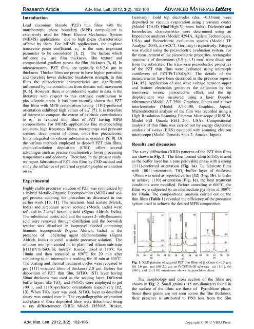
The x-ray diffraction (XRD) patterns <strong>of</strong> the <strong>PZT</strong> <strong>thin</strong> <strong>films</strong><br />
are shown in Fig. 1. The <strong>films</strong> formed when SrTiO3 is used<br />
as the buffer layer has a pure perovskite phase <strong>with</strong> a strong<br />
{111}-preferred orientation (Fig. 1a). To fabricate <strong>films</strong><br />
<strong>with</strong> {001}-orientation, TiO2 buffer layer <strong>of</strong> thickness<br />
~30nm was used as reported earlier [12] (Fig. 1b). In order<br />
to achieve {110}-orientation (Fig. 1c), the heat treatment<br />
conditions were modified. Before annealing at 600 0 C, the<br />
<strong>films</strong> were subjected to an intermediate pyrolysis at 300 0 C<br />
for 10min. The compositional analysis carried out on the<br />
<strong>thin</strong> <strong>films</strong> (Table 1) revealed the efficiency <strong>of</strong> the precursor<br />
system used to achieve the desired MPB composition.<br />
Fig. 1. XRD patterns <strong>of</strong> textured <strong>PZT</strong> <strong>thin</strong> <strong>films</strong> <strong>of</strong> thickness (i) 0.5 m;<br />
(ii) 1.0 m, and (iii) 2.0 m on Pt/Ti/SiO2/Si substrate (a) {111}, (b)<br />
{001}, and (c) {110} orientation :shows the pyrochlore phase.<br />
The morphology and cross section <strong>of</strong> the <strong>films</strong> are<br />
shown in Fig. 2. Small grains (~15 nm diameter) found in<br />
the surface <strong>of</strong> the <strong>films</strong> are those <strong>of</strong> Pyrochlore phase.<br />
Since these grains are not seen across the film thickness,<br />
their presence is attributed to PbO loss from the film<br />
Adv. Mat. Lett. 2012, 3(2), 102-106 Copyright © 2012 VBRI Press