Synthesis of carbon nanowires by SHI irradiation of fullerene C70 ...
Synthesis of carbon nanowires by SHI irradiation of fullerene C70 ...
Synthesis of carbon nanowires by SHI irradiation of fullerene C70 ...

Create successful ePaper yourself
Turn your PDF publications into a flip-book with our unique Google optimized e-Paper software.
Introduction<br />
Electrically conducting <strong>nanowires</strong> are potential candidates<br />
for application in flat panel display devices due to their<br />
interesting field emission properties [1–2]. An array <strong>of</strong><br />
parallel conducting <strong>nanowires</strong> in some insulating matrix is a<br />
good substitute for electron emitters in order to increase the<br />
pixel density in display devices. Several methods have been<br />
developed for the fabrication <strong>of</strong> <strong>nanowires</strong> arrays including<br />
catalytic growth [3], template methods [4,5], Langmuir<br />
Blodgett and electrospinning [6]. The important aspect for<br />
the creation <strong>of</strong> <strong>nanowires</strong> is the development <strong>of</strong> new<br />
methods which can provide large scale and controllable<br />
production <strong>of</strong> these <strong>nanowires</strong>, especially for aligned<br />
<strong>nanowires</strong>. The electron beam lithography can help in the<br />
formation <strong>of</strong> catalyst sites for aligned production <strong>of</strong><br />
<strong>nanowires</strong>, but this serial technique is too slow for scalable<br />
mass production.<br />
Ion beam methods are interesting because <strong>of</strong> its unique<br />
feature <strong>of</strong> depositing large electronic energy (for swift<br />
heavy ions) in a confined cylindrical nanozone in a<br />
controlled fashion. Ion beam <strong>irradiation</strong> is known to be a<br />
valuable and innovative tool for engineering and<br />
modification <strong>of</strong> materials at nano/atomic scale. Swift heavy<br />
ions (ions having velocities close to or higher than the<br />
orbital electron velocity) passing through materials lose<br />
energy along their path dominantly to the electronic<br />
subsystem and each ion induces damages in the material<br />
within diameters <strong>of</strong> several nanometers width. Carbon<br />
<strong>nanowires</strong>/nanochannels have successfully been<br />
synthesized using swift heavy ion <strong>irradiation</strong> in <strong>fullerene</strong><br />
C60 and some polymer thin films [7-9]. In a comparative<br />
study <strong>of</strong> structural stability <strong>of</strong> <strong>fullerene</strong> C60 and <strong>C70</strong> with<br />
swift heavy ion <strong>irradiation</strong>, it has been shown that <strong>fullerene</strong><br />
<strong>C70</strong> molecule is marginally stable than <strong>fullerene</strong> C60 against<br />
swift heavy ion <strong>irradiation</strong> [10]. The radius <strong>of</strong> ion track was<br />
found to be higher for <strong>fullerene</strong> C60 than that <strong>of</strong> <strong>C70</strong> for<br />
same electronic energy loss. Also the polymerization <strong>of</strong><br />
<strong>fullerene</strong> C60 at low fluences has been reported many times<br />
[11-12] which was a major cause for the mismatch between<br />
the fluence and ion track areal density. There is no such<br />
polymerization has been reported so far in <strong>C70</strong> and therefore<br />
<strong>C70</strong> is another interesting material to form <strong>carbon</strong> <strong>nanowires</strong><br />
using swift heavy ion <strong>irradiation</strong> technique. Therefore, swift<br />
heavy ion <strong>irradiation</strong> has been used in present work to<br />
synthesize conducing <strong>carbon</strong> <strong>nanowires</strong> in <strong>fullerene</strong> <strong>C70</strong><br />
matrix. To the best <strong>of</strong> our knowledge, first time conducting<br />
<strong>nanowires</strong> are synthesized in <strong>fullerene</strong> <strong>C70</strong> films <strong>by</strong> our<br />
group. Fullerene, having resistivity almost like insulators<br />
becomes conducting due to its transformation into<br />
amorphous <strong>carbon</strong> within ion track region [13-16] and in<br />
this manner, conduction <strong>nanowires</strong> <strong>of</strong> amorphous <strong>carbon</strong><br />
can be formed in insulating <strong>fullerene</strong> matrix.<br />
Experimental<br />
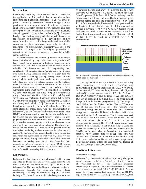
Fullerene <strong>C70</strong> thin films with a thickness <strong>of</strong> ~200 nm were<br />
deposited on 50 nm thick Au layers on glass substrate. The<br />
need to deposit Au layer between glass substrate and<br />
<strong>fullerene</strong> <strong>C70</strong> film was to facilitate the characterization <strong>of</strong><br />
conducting channels <strong>by</strong> conducting atomic force<br />
microscopy (C-AFM), as shown in Fig. 1. Therefore,<br />
initially a 50 nm Au films were deposited on glass substrate<br />
Singhal, Tripathi and Avasthi<br />
<strong>by</strong> resistive heating and above it, <strong>fullerene</strong> <strong>C70</strong> film was<br />
deposited <strong>by</strong> sublimation <strong>of</strong> <strong>C70</strong> pellet. The pellet was made<br />
from <strong>C70</strong> powder (Alfa Aesar 99.9 %) <strong>by</strong> applying suitable<br />
pressure on it in a 3 mm thick dye. The base pressure in the<br />
chamber before and after the evaporation was 7 x 10 -7 and<br />
3 x 10 -6 torr respectively. The deposition was performed <strong>by</strong><br />
sublimation <strong>of</strong> <strong>C70</strong> pellet at a rate <strong>of</strong> ~ 1.0 nm/sec and <strong>by</strong><br />
passing a current <strong>of</strong> 170 A in a W boat. A Quartz crystal<br />
oscillator was used to measure the thickness <strong>of</strong> the film<br />
during deposition. A small area <strong>of</strong> the Au film was masked<br />
so that it can be used as a contact for C-AFM<br />
measurements.<br />
Fig. 1. Schematic showing the arrangements for the measurements <strong>of</strong><br />
current across the <strong>nanowires</strong><br />
The <strong>C70</strong> thin films were irradiated with 100 MeV Ag<br />
ions at fluences <strong>of</strong> 1x10 9 , 3x10 9 , and 1x10 10 ions/cm 2 using<br />
15 UD tandem Pelletron accelerator at IUAC, New Delhi.<br />
In the case <strong>of</strong> 100 MeV Ag ions, the electronic (Se) and<br />
nuclear (Sn) energy losses in <strong>C70</strong> are ~ 1.2 x 10 3 eV/Å and ~<br />
15.4 eV/Å respectively and the range <strong>of</strong> Ag ions in <strong>C70</strong> is<br />
15.6 m as calculated <strong>by</strong> SRIM 2003 (The Stopping and<br />
Range <strong>of</strong> Ions in Matter) programme [17]. The range is<br />
much higher than the thickness <strong>of</strong> the film (~ 200 nm) so<br />
that all the ions are buried inside the substrate after<br />
depositing energy into the <strong>fullerene</strong> film. The electronic<br />
energy loss in the entire thickness <strong>of</strong> the film is uniform, as<br />
estimated <strong>by</strong> the SRIM simulation. The fluences were kept<br />
low, so as to avoid the overlap <strong>of</strong> the ion tracks. The ion<br />
beam was scanned in area <strong>of</strong> 1 x 1 cm 2 <strong>by</strong> an<br />
electromagnetic scanner. The C-AFM measurements were<br />
performed on the irradiated and pristine samples using the<br />
instrument Nanoscope III a SPM. The I-V measurements in<br />
C-AFM mode were also performed on the irradiated<br />
samples. Micro-Raman data <strong>of</strong> as-deposited film was<br />
recorded with a Renishaw in-Via Raman microscope using<br />
Ar ion laser excitation at 514 nm and at room temperature.<br />
To avoid any heating effect, the laser beam was focused at<br />
very low power (< 2 mW, 20 X objective).<br />
Results and discussion<br />
Raman spectroscopy<br />
Fullerene <strong>C70</strong> molecule is <strong>of</strong> reduced symmetry (D5h point<br />
group) compared to <strong>fullerene</strong> C60 and therefore the number<br />
<strong>of</strong> vibrational modes <strong>of</strong> this molecule increases<br />
dramatically. For pure <strong>C70</strong> at room temperature, 53 Raman<br />
active modes are predicted (12 A1' +22 E2' +19 E1") from<br />
group theory and various first principle theories [18-19].<br />
Fig. 2 depicts the typical Raman spectra <strong>of</strong> a pure <strong>C70</strong> thin<br />
Adv. Mat. Lett. 2013, 4(6), 413-417 Copyright © 2013 VBRI press 414