Synthesis of carbon nanowires by SHI irradiation of fullerene C70 ...
Synthesis of carbon nanowires by SHI irradiation of fullerene C70 ...
Synthesis of carbon nanowires by SHI irradiation of fullerene C70 ...

Create successful ePaper yourself
Turn your PDF publications into a flip-book with our unique Google optimized e-Paper software.
fluences and compared them with those calculated<br />
theoretically <strong>by</strong> taking the value <strong>of</strong> ion track diameter from<br />
our previous work [16]. These values are given in Table 1.<br />
Experimental value for number <strong>of</strong> tracks is the average<br />
value taken over 3 - 4 different areas <strong>of</strong> 2D current images.<br />
There is some mismatch between theoretical and<br />
experimental values for number <strong>of</strong> ion tracks, which may be<br />
due to the following reasons: (i) a small mismatch is<br />
possible because <strong>of</strong> the fluence uncertainty (maximux up to<br />
20%) as ion beam current can have some small variation<br />
during the <strong>irradiation</strong> time period, (ii) since the ion hits<br />
randomly, it is possible that some ion tracks are either<br />
overlapping or probed simultaneously due to close<br />
proximity <strong>of</strong> two tracks, (iii) the finite size <strong>of</strong> tip may have<br />
influence, (iv) possibility <strong>of</strong> lateral conduction with the<br />
neighbouring tracks.<br />
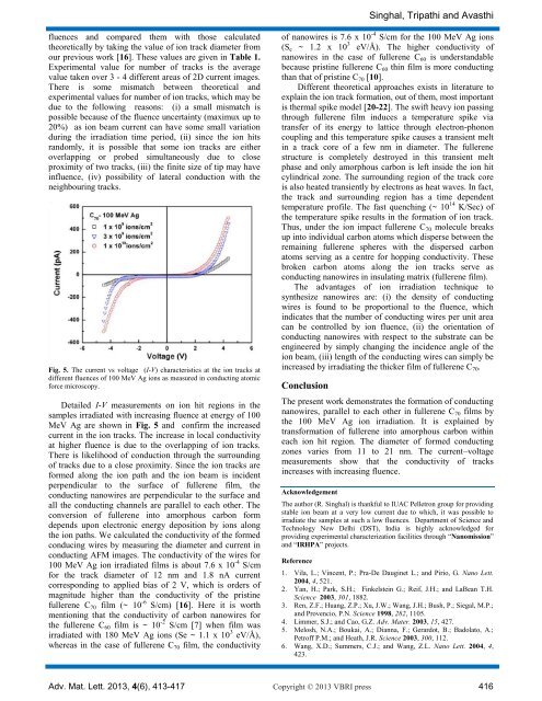
Fig. 5. The current vs voltage (I-V) characteristics at the ion tracks at<br />
different fluences <strong>of</strong> 100 MeV Ag ions as measured in conducting atomic<br />
force microscopy.<br />
Detailed I-V measurements on ion hit regions in the<br />
samples irradiated with increasing fluence at energy <strong>of</strong> 100<br />
MeV Ag are shown in Fig. 5 and confirm the increased<br />
current in the ion tracks. The increase in local conductivity<br />
at higher fluence is due to the overlapping <strong>of</strong> ion tracks.<br />
There is likelihood <strong>of</strong> conduction through the surrounding<br />
<strong>of</strong> tracks due to a close proximity. Since the ion tracks are<br />
formed along the ion path and the ion beam is incident<br />
perpendicular to the surface <strong>of</strong> <strong>fullerene</strong> film, the<br />
conducting <strong>nanowires</strong> are perpendicular to the surface and<br />
all the conducting channels are parallel to each other. The<br />
conversion <strong>of</strong> <strong>fullerene</strong> into amorphous <strong>carbon</strong> form<br />
depends upon electronic energy deposition <strong>by</strong> ions along<br />
the ion paths. We calculated the conductivity <strong>of</strong> the formed<br />
conducing wires <strong>by</strong> measuring the diameter and current in<br />
conducting AFM images. The conductivity <strong>of</strong> the wires for<br />
100 MeV Ag ion irradiated films is about 7.6 x 10 -4 S/cm<br />
for the track diameter <strong>of</strong> 12 nm and 1.8 nA current<br />
corresponding to applied bias <strong>of</strong> 2 V, which is orders <strong>of</strong><br />
magnitude higher than the conductivity <strong>of</strong> the pristine<br />
<strong>fullerene</strong> <strong>C70</strong> film (~ 10 -6 S/cm) [16]. Here it is worth<br />
mentioning that the conductivity <strong>of</strong> <strong>carbon</strong> <strong>nanowires</strong> for<br />
the <strong>fullerene</strong> C60 film is ~ 10 -2 S/cm [7] when film was<br />
irradiated with 180 MeV Ag ions (Se ~ 1.1 x 10 3 eV/Å),<br />
whereas in the case <strong>of</strong> <strong>fullerene</strong> <strong>C70</strong> film, the conductivity<br />
Singhal, Tripathi and Avasthi<br />
<strong>of</strong> <strong>nanowires</strong> is 7.6 x 10 -4 S/cm for the 100 MeV Ag ions<br />
(Se ~ 1.2 x 10 3 eV/Å). The higher conductivity <strong>of</strong><br />
<strong>nanowires</strong> in the case <strong>of</strong> <strong>fullerene</strong> C60 is understandable<br />
because pristine <strong>fullerene</strong> C60 thin film is more conducting<br />
than that <strong>of</strong> pristine <strong>C70</strong> [10].<br />
Different theoretical approaches exists in literature to<br />
explain the ion track formation, out <strong>of</strong> them, most important<br />
is thermal spike model [20-22]. The swift heavy ion passing<br />
through <strong>fullerene</strong> film induces a temperature spike via<br />
transfer <strong>of</strong> its energy to lattice through electron-phonon<br />
coupling and this temperature spike causes a transient melt<br />
in a track core <strong>of</strong> a few nm in diameter. The <strong>fullerene</strong><br />
structure is completely destroyed in this transient melt<br />
phase and only amorphous <strong>carbon</strong> is left inside the ion hit<br />
cylindrical zone. The surrounding region <strong>of</strong> the track core<br />
is also heated transiently <strong>by</strong> electrons as heat waves. In fact,<br />
the track and surrounding region has a time dependent<br />
temperature pr<strong>of</strong>ile. The fast quenching (~ 10 14 K/Sec) <strong>of</strong><br />
the temperature spike results in the formation <strong>of</strong> ion track.<br />
Thus, under the ion impact <strong>fullerene</strong> <strong>C70</strong> molecule breaks<br />
up into individual <strong>carbon</strong> atoms which disperse between the<br />
remaining <strong>fullerene</strong> spheres with the dispersed <strong>carbon</strong><br />
atoms serving as a centre for hopping conductivity. These<br />
broken <strong>carbon</strong> atoms along the ion tracks serve as<br />
conducting <strong>nanowires</strong> in insulating matrix (<strong>fullerene</strong> film).<br />
The advantages <strong>of</strong> ion <strong>irradiation</strong> technique to<br />
synthesize <strong>nanowires</strong> are: (i) the density <strong>of</strong> conducting<br />
wires is found to be proportional to the fluence, which<br />
indicates that the number <strong>of</strong> conducting wires per unit area<br />
can be controlled <strong>by</strong> ion fluence, (ii) the orientation <strong>of</strong><br />
conducting <strong>nanowires</strong> with respect to the substrate can be<br />
engineered <strong>by</strong> simply changing the incidence angle <strong>of</strong> the<br />
ion beam, (iii) length <strong>of</strong> the conducting wires can simply be<br />
increased <strong>by</strong> irradiating the thicker film <strong>of</strong> <strong>fullerene</strong> <strong>C70</strong>.<br />
Conclusion<br />
The present work demonstrates the formation <strong>of</strong> conducting<br />
<strong>nanowires</strong>, parallel to each other in <strong>fullerene</strong> <strong>C70</strong> films <strong>by</strong><br />
the 100 MeV Ag ion <strong>irradiation</strong>. It is explained <strong>by</strong><br />
transformation <strong>of</strong> <strong>fullerene</strong> into amorphous <strong>carbon</strong> within<br />
each ion hit region. The diameter <strong>of</strong> formed conducting<br />
zones varies from 11 to 21 nm. The current–voltage<br />
measurements show that the conductivity <strong>of</strong> tracks<br />
increases with increasing fluence.<br />
Acknowledgement<br />
The author (R. Singhal) is thankful to IUAC Pelletron group for providing<br />
stable ion beam at a very low current due to which, it was possible to<br />
irradiate the samples at such a low fluences. Department <strong>of</strong> Science and<br />
Technology New Delhi (DST), India is highly acknowledged for<br />
providing experimental characterization facilities through “Nanomission”<br />
and “IRHPA” projects.<br />
Reference<br />
1. Vila, L.; Vincent, P.; Pra-De Dauginet L.; and Pirio, G. Nano Lett.<br />
2004, 4, 521.<br />
2. Yan, H.; Park, S.H.; Finkelstein G.; Reif, J.H.; and LaBean T.H.<br />
Science 2003, 301, 1882.<br />
3. Ren, Z.F.; Huang, Z.P.; Xu, J.W.; Wang, J.H.; Bush, P.; Siegal, M.P.;<br />
and Provencio, P.N. Science 1998, 282, 1105.<br />
4. Limmer, S.J.; and Cao, G.Z. Adv. Mater. 2003, 15, 427.<br />
5. Melosh, N.A.; Boukai, A.; Dianna, F.; Gerardot, B.; Badolato, A.;<br />
Petr<strong>of</strong>f P.M.; and Heath, J.R. Science 2003, 300, 112.<br />
6. Wang, X.D.; Summers, C.J.; and Wang, Z.L. Nano Lett. 2004, 4,<br />
423.<br />
Adv. Mat. Lett. 2013, 4(6), 413-417 Copyright © 2013 VBRI press 416