Effect of copper on composition, structural and optical properties of ...
Effect of copper on composition, structural and optical properties of ...
Effect of copper on composition, structural and optical properties of ...

Create successful ePaper yourself
Turn your PDF publications into a flip-book with our unique Google optimized e-Paper software.
Film preparati<strong>on</strong><br />
The depositi<strong>on</strong> <str<strong>on</strong>g>of</str<strong>on</strong>g> <str<strong>on</strong>g>copper</str<strong>on</strong>g> <strong>and</strong> ZnTe were d<strong>on</strong>e in two<br />
separate depositi<strong>on</strong> cycles. The depositi<strong>on</strong> were carried out<br />
in vacuum better than 10 -5 m.bar, inside a 12 inch vacuum<br />
chamber (HINDHIVAC 12A4D). Initially <str<strong>on</strong>g>copper</str<strong>on</strong>g> (99.99%,<br />
Aldrich) films <str<strong>on</strong>g>of</str<strong>on</strong>g> thickness (250 Å) were deposited over the<br />
well-cleaned glass substrates by vacuum evaporati<strong>on</strong><br />
technique. Then ZnTe (99.99%, Aldrich) films <str<strong>on</strong>g>of</str<strong>on</strong>g><br />
thicknesses (650, 1400 <strong>and</strong> 3300Å) were deposited over the<br />
pre-deposited <str<strong>on</strong>g>copper</str<strong>on</strong>g> films (250 Å) at room temperature. A<br />
rotary drive was employed to maintain uniformity in film<br />
thickness <strong>and</strong> to get well diffusi<strong>on</strong> <str<strong>on</strong>g>of</str<strong>on</strong>g> <str<strong>on</strong>g>copper</str<strong>on</strong>g> into ZnTe the<br />
samples were annealed in a hot air oven at 100˚C for 2<br />
hours.<br />
Measurements<br />
Thickness <str<strong>on</strong>g>of</str<strong>on</strong>g> the films was measured by quartz crystal<br />
m<strong>on</strong>itor (“Hind Hivac” Digital Thickness M<strong>on</strong>tor Model–<br />
DTM–101), <strong>and</strong> verified by multiple beam interferometer<br />
(MBI) technique by forming Fizeau fringes [21]. Energy<br />
Dispersive Analysis <str<strong>on</strong>g>of</str<strong>on</strong>g> X-rays (EDAX) (JOEL 840<br />
SEM/EDAX) was employed for the c<strong>on</strong>firmati<strong>on</strong> <str<strong>on</strong>g>of</str<strong>on</strong>g><br />
compositi<strong>on</strong> <str<strong>on</strong>g>of</str<strong>on</strong>g> thin films. The <strong>structural</strong> aspects <str<strong>on</strong>g>of</str<strong>on</strong>g> the<br />
films were analyzed, using X-ray diffractometer with<br />
filtered CuKα radiati<strong>on</strong> (λ = 1.5418 Å). The <strong>optical</strong><br />
transmittance spectra <str<strong>on</strong>g>of</str<strong>on</strong>g> these films were recorded using a<br />
UV–VIS-NIR spectrophotometer (Jasco Corp., V-570) in<br />
the range 200 – 2500 nm with 1 nm resoluti<strong>on</strong> at room<br />
temperature.<br />
Table 1. Atomic percentage <str<strong>on</strong>g>of</str<strong>on</strong>g> Zn, Te <strong>and</strong> Cu for <str<strong>on</strong>g>copper</str<strong>on</strong>g> doped ZnTe thin<br />
films for thicknesses 650 Å <strong>and</strong> 3300Å.<br />
Element 650 Å 3300 Å<br />
Results <strong>and</strong> discussi<strong>on</strong><br />
EDAX analysis<br />
Zn 59.33 59.03<br />
Te 17.76 40.97<br />
Cu 22.91 0.00<br />
The analyzed atomic percentage values <str<strong>on</strong>g>of</str<strong>on</strong>g> elements Zn, Te<br />
<strong>and</strong> Cu in the above films are presented in Table 1. From<br />
this Table, it is c<strong>on</strong>cluded that tellurium is replaced by<br />
<str<strong>on</strong>g>copper</str<strong>on</strong>g>. Due to this reas<strong>on</strong> the atomic percentage <str<strong>on</strong>g>of</str<strong>on</strong>g><br />
tellurium is decreased in ZnTe film <str<strong>on</strong>g>of</str<strong>on</strong>g> thickness 650 Å<br />
deposited <strong>on</strong> the pre-deposited <str<strong>on</strong>g>copper</str<strong>on</strong>g> film. But at higher<br />
ZnTe film thickness (3300 Å), the EDAX analysis shows<br />
zero atomic percentage <str<strong>on</strong>g>of</str<strong>on</strong>g> <str<strong>on</strong>g>copper</str<strong>on</strong>g>. From this, it is<br />
c<strong>on</strong>cluded that all the <str<strong>on</strong>g>copper</str<strong>on</strong>g> atoms were diffused into the<br />
ZnTe films without desorpti<strong>on</strong> from the substrate during the<br />
ZnTe depositi<strong>on</strong>. This is also c<strong>on</strong>firmed by XRD analysis.<br />
XRD analysis<br />
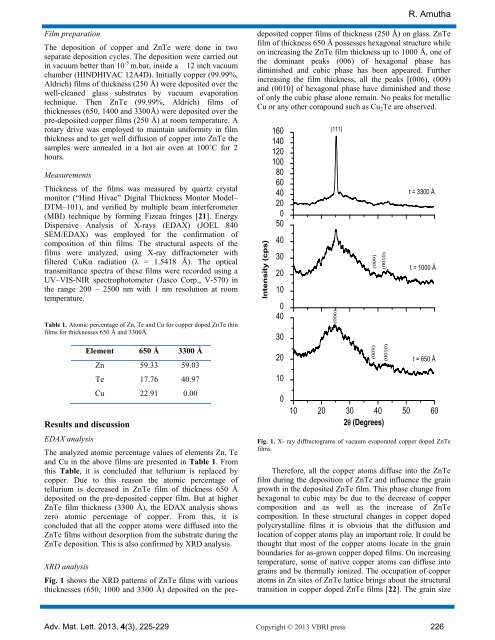
Fig. 1 shows the XRD patterns <str<strong>on</strong>g>of</str<strong>on</strong>g> ZnTe films with various<br />
thicknesses (650, 1000 <strong>and</strong> 3300 Å) deposited <strong>on</strong> the pre-<br />
R. Amutha<br />
deposited <str<strong>on</strong>g>copper</str<strong>on</strong>g> films <str<strong>on</strong>g>of</str<strong>on</strong>g> thickness (250 Å) <strong>on</strong> glass. ZnTe<br />
film <str<strong>on</strong>g>of</str<strong>on</strong>g> thickness 650 Å possesses hexag<strong>on</strong>al structure while<br />
<strong>on</strong> increasing the ZnTe film thickness up to 1000 Å, <strong>on</strong>e <str<strong>on</strong>g>of</str<strong>on</strong>g><br />
the dominant peaks (006) <str<strong>on</strong>g>of</str<strong>on</strong>g> hexag<strong>on</strong>al phase has<br />
diminished <strong>and</strong> cubic phase has been appeared. Further<br />
increasing the film thickness, all the peaks [(006), (009)<br />
<strong>and</strong> (0010] <str<strong>on</strong>g>of</str<strong>on</strong>g> hexag<strong>on</strong>al phase have diminished <strong>and</strong> those<br />
<str<strong>on</strong>g>of</str<strong>on</strong>g> <strong>on</strong>ly the cubic phase al<strong>on</strong>e remain. No peaks for metallic<br />
Cu or any other compound such as Cu2Te are observed.<br />
10 20 30 40 50 60<br />
2 (Degrees)<br />
Adv. Mat. Lett. 2013, 4(3), 225-229 Copyright © 2013 VBRI press 226<br />
Intensity (cps)<br />
160<br />
140<br />
120<br />
100<br />
80<br />
60<br />
40<br />
20<br />
0<br />
50<br />
40<br />
30<br />
20<br />
10<br />
0<br />
40<br />
30<br />
20<br />
10<br />
0<br />
(006)<br />
(111)<br />
(009)<br />
(009)<br />
(0010)<br />
(0010)<br />
t = 3300 Å<br />
t = 1000 Å<br />
t = 650 Å<br />
Fig. 1. X- ray diffractograms <str<strong>on</strong>g>of</str<strong>on</strong>g> vacuum evaporated <str<strong>on</strong>g>copper</str<strong>on</strong>g> doped ZnTe<br />
films.<br />
Therefore, all the <str<strong>on</strong>g>copper</str<strong>on</strong>g> atoms diffuse into the ZnTe<br />
film during the depositi<strong>on</strong> <str<strong>on</strong>g>of</str<strong>on</strong>g> ZnTe <strong>and</strong> influence the grain<br />
growth in the deposited ZnTe film. This phase change from<br />
hexag<strong>on</strong>al to cubic may be due to the decrease <str<strong>on</strong>g>of</str<strong>on</strong>g> <str<strong>on</strong>g>copper</str<strong>on</strong>g><br />
compositi<strong>on</strong> <strong>and</strong> as well as the increase <str<strong>on</strong>g>of</str<strong>on</strong>g> ZnTe<br />
compositi<strong>on</strong>. In these <strong>structural</strong> changes in <str<strong>on</strong>g>copper</str<strong>on</strong>g> doped<br />
polycrystalline films it is obvious that the diffusi<strong>on</strong> <strong>and</strong><br />
locati<strong>on</strong> <str<strong>on</strong>g>of</str<strong>on</strong>g> <str<strong>on</strong>g>copper</str<strong>on</strong>g> atoms play an important role. It could be<br />
thought that most <str<strong>on</strong>g>of</str<strong>on</strong>g> the <str<strong>on</strong>g>copper</str<strong>on</strong>g> atoms locate in the grain<br />
boundaries for as-grown <str<strong>on</strong>g>copper</str<strong>on</strong>g> doped films. On increasing<br />
temperature, some <str<strong>on</strong>g>of</str<strong>on</strong>g> native <str<strong>on</strong>g>copper</str<strong>on</strong>g> atoms can diffuse into<br />
grains <strong>and</strong> be thermally i<strong>on</strong>ized. The occupati<strong>on</strong> <str<strong>on</strong>g>of</str<strong>on</strong>g> <str<strong>on</strong>g>copper</str<strong>on</strong>g><br />
atoms in Zn sites <str<strong>on</strong>g>of</str<strong>on</strong>g> ZnTe lattice brings about the <strong>structural</strong><br />
transiti<strong>on</strong> in <str<strong>on</strong>g>copper</str<strong>on</strong>g> doped ZnTe films [22]. The grain size