Effect of copper on composition, structural and optical properties of ...
Effect of copper on composition, structural and optical properties of ...
Effect of copper on composition, structural and optical properties of ...

Create successful ePaper yourself
Turn your PDF publications into a flip-book with our unique Google optimized e-Paper software.
where T0 is the transmittance <strong>and</strong> t the thickness <str<strong>on</strong>g>of</str<strong>on</strong>g> the film.<br />
( h) 2 (eV/cm) 2<br />
( h) 2 (eV/cm) 2<br />
( h) 2 (eV/cm) 2<br />
1.0x10 16<br />
5.0x10 15<br />
t = 6 5 0 Å<br />
0.0<br />
0.0 0.4 0.8 1.2 1.6 2.0 2.4 2.8<br />
4x10 15<br />
3x10 15<br />
2x10 15<br />
1x10 15<br />
5x10 14<br />
4x10 14<br />
3x10 14<br />
2x10 14<br />
1x10 14<br />
(a)<br />
(b)<br />
h ( e V )<br />
t = 1 0 0 0 Å<br />
0<br />
0.0 0.4 0.8 1.2 1.6 2.0 2.4 2.8<br />
(c)<br />
h ( e V )<br />
t = 3 3 0 0 Å<br />
0<br />
0.0 0.4 0.8 1.2 1.6 2.0 2.4 2.8<br />
h ( e V )<br />
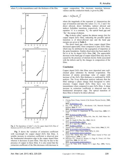
Fig. 4. The dependence <str<strong>on</strong>g>of</str<strong>on</strong>g> (αhυ) 2 vs hυ for <str<strong>on</strong>g>copper</str<strong>on</strong>g> doped ZnTe films <str<strong>on</strong>g>of</str<strong>on</strong>g><br />
thickness (a) 650 Å, (b) 1000 Å <strong>and</strong> c) 3300 Å.<br />
Fig. 3 shows the variati<strong>on</strong> <str<strong>on</strong>g>of</str<strong>on</strong>g> extincti<strong>on</strong> coefficient<br />
with wavelength for <str<strong>on</strong>g>copper</str<strong>on</strong>g> doped ZnTe thin films. A<br />
notable increase in extincti<strong>on</strong> coefficient is observed near<br />
the fundamental absorpti<strong>on</strong> edge in the <str<strong>on</strong>g>copper</str<strong>on</strong>g> doped films<br />
whereas it decreases in pure films. This may be due to the<br />
presence <str<strong>on</strong>g>of</str<strong>on</strong>g> <str<strong>on</strong>g>copper</str<strong>on</strong>g> in those films. It is also noted that the<br />
extincti<strong>on</strong> coefficient <str<strong>on</strong>g>of</str<strong>on</strong>g> the film decreases with decrease in<br />
R. Amutha<br />
<str<strong>on</strong>g>copper</str<strong>on</strong>g> compositi<strong>on</strong>. The electr<strong>on</strong>ic transiti<strong>on</strong> between<br />
valence <strong>and</strong> the c<strong>on</strong>ducti<strong>on</strong> b<strong>and</strong>s, is given by [35]-<br />
P<br />
αhυ = A hυ-E g<br />
where the magnitude <str<strong>on</strong>g>of</str<strong>on</strong>g> the exp<strong>on</strong>ent ‘p’ characterizes the<br />
type <str<strong>on</strong>g>of</str<strong>on</strong>g> transiti<strong>on</strong> <strong>and</strong> takes the values 1/2, 3/2, 2 <strong>and</strong> 3 for<br />
direct allowed, direct forbidden, indirect allowed <strong>and</strong><br />
indirect forbidden transiti<strong>on</strong>s respectively. In the above<br />
equati<strong>on</strong> ‘A’ is a c<strong>on</strong>stant, ‘Eg’ the <strong>optical</strong> b<strong>and</strong> gap <strong>and</strong><br />
‘ hυ ’ the energy <str<strong>on</strong>g>of</str<strong>on</strong>g> phot<strong>on</strong>.<br />
Fig. 4 shows (αhυ) 2 against the phot<strong>on</strong> energy (hυ) for<br />
<str<strong>on</strong>g>copper</str<strong>on</strong>g> doped ZnTe films, indicating the possible <strong>optical</strong><br />
transiti<strong>on</strong> is <str<strong>on</strong>g>of</str<strong>on</strong>g> direct-allowed type <strong>and</strong> the b<strong>and</strong> gap<br />
energies are given in Table 2.<br />
The direct b<strong>and</strong> gap values these <str<strong>on</strong>g>copper</str<strong>on</strong>g> doped films<br />
decreased appreciably when compared to pure ZnTe films,<br />
which may be attributed to the segregati<strong>on</strong> <str<strong>on</strong>g>of</str<strong>on</strong>g> impurities at<br />
the grain boundaries. Similar observati<strong>on</strong> has been made by<br />
Pal et al for In doped ZnTe films [36]. The appreciable<br />
decrease in the b<strong>and</strong> gap <str<strong>on</strong>g>of</str<strong>on</strong>g> <str<strong>on</strong>g>copper</str<strong>on</strong>g> doped films may also be<br />
caused by the presence <str<strong>on</strong>g>of</str<strong>on</strong>g> internal electric fields associated<br />
with the defects <strong>and</strong> by the changes in compositi<strong>on</strong> <str<strong>on</strong>g>of</str<strong>on</strong>g> the<br />
films.<br />
C<strong>on</strong>clusi<strong>on</strong><br />
Copper doped ZnTe thin films were deposited <strong>on</strong>to wellcleaned<br />
glass substrates by thermal evaporati<strong>on</strong>. The<br />
decrease <str<strong>on</strong>g>of</str<strong>on</strong>g> atomic percentage value <str<strong>on</strong>g>of</str<strong>on</strong>g> <str<strong>on</strong>g>copper</str<strong>on</strong>g> with<br />
increase <str<strong>on</strong>g>of</str<strong>on</strong>g> the ZnTe film thickness is c<strong>on</strong>firmed by EDX<br />
analysis. The X-ray diffracti<strong>on</strong> analysis indicates that the<br />
films undergo a phase change from hexag<strong>on</strong>al to cubic<br />
structure. Copper doped ZnTe films have very low<br />
transmittance when compared to pure ZnTe films. A sharp<br />
increase in extincti<strong>on</strong> coefficient is observed near the<br />
fundamental absorpti<strong>on</strong> edge. The <strong>optical</strong> transiti<strong>on</strong> <str<strong>on</strong>g>of</str<strong>on</strong>g><br />
these films is found to be direct allowed.<br />
Reference<br />
1. Cho<strong>on</strong>g Hyun Chung. Journal <str<strong>on</strong>g>of</str<strong>on</strong>g> the Korean Physical Society. 1969,<br />
2, 462.<br />
DOI: 10.3938/jkps.1.112<br />
2. Rao, G.K.; Bangera, K.V.; Shivakumar. G.K. Materials Research<br />
Bulletin. 2010, 45, 1357.<br />
DOI: 10.1016/j.materresbull.2010.06.050<br />
3. Baratii, A.; Klein, A.; Jaegermann, W. Thin Solid Films. 2009, 517,<br />
2149<br />
DOI: 10.1016/j.tsf.2008.10.078<br />
4. Mazumdar, N.; Sarma, R.; Sarma, B.K.; Das, H.L. Bull. Mater. Sci.<br />
2006, 29(1) 11.<br />
5. Aven, M.; Segall, B. Phys. Rev. 1963, 130, 81.<br />
DOI: 10.1103/PhysRev.130.81<br />
6. Aven, M. J. Appl. Phys. 1967, 38, 4421.<br />
DOI: 10.1063/1.1709141<br />
7. Thomas, D.G.; Sadowski, E.A. J. Phys. Chem. Solids. 1964, 25, 395.<br />
DOI: 10.1016/0022-3697(64)90005-8<br />
8. Smith, F.T.J. J. Phys. Chem. Solids. 1971, 32, 2201.<br />
DOI: 10.1016/S0022-3697(71)80398-0<br />
9. Kalita, P.K.; Sarma, B.K.; Das, H.L. Indian Journal <str<strong>on</strong>g>of</str<strong>on</strong>g> Pure <strong>and</strong><br />
Applied Physics. 1999, 37, 885.<br />
10. BaEtzner, D.L.; Wendt, R.; Romeo, A.; Zogg, H.; Tiwari, A.N. Thin<br />
Solid Films. 2000, 361-362, 463.<br />
DOI: 10.1016/S0040-6090(99)00842-1<br />
11. Rioux, D.; Niles, D.W.; Hochst, H. J. Appl. Phys. 1993, 73(12),<br />
8381.<br />
Adv. Mat. Lett. 2013, 4(3), 225-229 Copyright © 2013 VBRI press 228