Intel 45nm Process Overview - UCSB CAD & Test
Intel 45nm Process Overview - UCSB CAD & Test
Intel 45nm Process Overview - UCSB CAD & Test

Create successful ePaper yourself
Turn your PDF publications into a flip-book with our unique Google optimized e-Paper software.
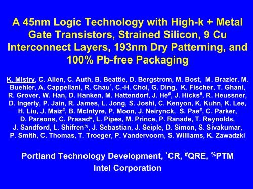
A <strong>45nm</strong> Logic Technology with High-k + Metal<br />
Gate Transistors, Strained Silicon, 9 Cu<br />
Interconnect Layers, 193nm Dry Patterning, and<br />
100% Pb-free Packaging<br />
K. Mistry, C. Allen, C. Auth, B. Beattie, D. Bergstrom, M. Bost, M. Brazier, M.<br />
Buehler, A. Cappellani, R. Chau * , C.-H. Choi, G. Ding, K. Fischer, T. Ghani,<br />
R. Grover, W. Han, D. Hanken, M. Hattendorf, J. He # , J. Hicks # , R. Heussner,<br />
D. Ingerly, P. Jain, R. James, L. Jong, S. Joshi, C. Kenyon, K. Kuhn, K. Lee,<br />
H. Liu, J. Maiz # , B. McIntyre, P. Moon, J. Neirynck, S. Pae # , C. Parker,<br />
D. Parsons, C. Prasad # , L. Pipes, M. Prince, P. Ranade, T. Reynolds,<br />
J. Sandford, L. Shifren % , J. Sebastian, J. Seiple, D. Simon, S. Sivakumar,<br />
P. Smith, C. Thomas, T. Troeger, P. Vandervoorn, S. Williams, K. Zawadzki<br />
Portland Technology Development, * CR, # QRE, % PTM<br />
<strong>Intel</strong> Corporation
Outline<br />
• Introduction<br />
• <strong>Process</strong> Features<br />
• Transistors<br />
• Interconnects<br />
• Manufacturing<br />
• Conclusions<br />
2
Introduction<br />
• SiON scaling running out of atoms<br />
• Poly depletion limits inversion T OX scaling<br />
Electrical (Inv) Tox (nm)<br />
10<br />
1<br />
Poly<br />
SiON<br />
Silicon<br />
350nm 250nm 180nm 130nm 90nm 65nm<br />
1000<br />
100<br />
10<br />
1<br />
0.1<br />
0.01<br />
Gate Leakage (Rel.)<br />
3
High-k + Metal Gate Benefits<br />
• High-k gate dielectric<br />
– Reduced gate leakage<br />
– T OX scaling<br />
• Metal gates<br />
– Eliminate polysilicon depletion<br />
– Resolves V T pinning and poor mobility<br />
for high-k dielectrics<br />
4
High-k + Metal Gate Challenges<br />
• High-k gate dielectric<br />
– Poor mobility, V T pinning due to soft<br />
optical phonons<br />
– Poor reliability<br />
• Metal gates<br />
– Dual bandedge workfunctions<br />
– Thermal stability<br />
– Integration scheme<br />
5
Outline<br />
• Introduction<br />
• <strong>Process</strong> Features<br />
• Transistors<br />
• Interconnects<br />
• Manufacturing<br />
• Conclusions<br />
6
<strong>Process</strong> Features<br />
• 45 nm Groundrules<br />
• 193 nm Dry Lithography<br />
• High-K + Metal Gate Transistors<br />
• 3 RD Generation Strained Silicon<br />
• Trench Contacts with Local Routing<br />
• 9 Cu Interconnect Layers<br />
• 100% Lead-free Packaging<br />
7
<strong>Process</strong> Features<br />
• 45 nm Groundrules<br />
• 193 nm Dry Lithography<br />
• High-K + Metal Gate Transistors<br />
• 3 RD Generation Strained Silicon<br />
• Trench Contacts with Local Routing<br />
• 9 Cu Interconnect Layers<br />
• 100% Lead-free Packaging<br />
8
<strong>45nm</strong> Design Rules<br />
Layer Pitch (nm) Thick (nm) Aspect Ratio<br />
Isolation 200 200<br />
Contacted Gate 160 60<br />
--<br />
Metal 1 160 144<br />
1.8<br />
Metal 2 160 144<br />
1.8<br />
Metal 3 160 144<br />
1.8<br />
Metal 4 240 216<br />
1.8<br />
Metal 5 280 252<br />
1.8<br />
Metal 6 360 324<br />
1.8<br />
Metal 7 560 504 1.8<br />
Metal 8 810 720 1.8<br />
Metal 9 30.5μm 7μm<br />
0.4<br />
~0.7x linear scaling from 65nm<br />
--<br />
9
Contacted Gate Pitch<br />
• Transistor gate pitch of 160 nm continues<br />
0.7x per generation scaling<br />
Contacted Gate Pitch (nm)<br />
1000<br />
100<br />
Pitch<br />
250nm 180nm 130nm 90nm 65nm <strong>45nm</strong><br />
Technology Node<br />
0.7x every<br />
2 years<br />
Tightest contacted gate pitch reported for 45 nm generation
SRAM Cells<br />
• 0.346 μm 2 and 0.382 μm 2 SRAM cells<br />
– Optimize density and power/performance<br />
SRAM Cell Size ( μm 2 )<br />
10<br />
1<br />
0.1<br />
250nm 180nm 130nm 90nm 65nm <strong>45nm</strong><br />
Technology Node<br />
0.5x every<br />
2 years<br />
Transistor density doubles every two years<br />
11
SRAM Array Density<br />
• SRAM array density achieves 1.9 Mb/mm 2<br />
SRAM Array Density (Mb/mm 2 )<br />
– Includes row/column drivers and other circuitry<br />
10.0<br />
1.0<br />
0.1<br />
1.9 Mb/mm 2<br />
90nm 65nm <strong>45nm</strong><br />
Array density scales at ~2X per generation<br />
12
Outline<br />
• Introduction<br />
• <strong>Process</strong> Features<br />
• Transistors<br />
• Interconnects<br />
• Manufacturing<br />
• Conclusions<br />
13
Transistor <strong>Process</strong> Flow<br />
• Key considerations<br />
– Integrate hafnium-based high-k dielectric,<br />
dual metal gate electrodes, strained silicon<br />
– Thermal stability of metal gate electrodes<br />
• High-k First, Metal Gate Last<br />
– Metal gate deposition after high temperature<br />
anneals<br />
– Integrated with strained silicon process<br />
– Transistor mask count same as 65nm<br />
14
Transistor <strong>Process</strong> Flow<br />
Dummy<br />
Polysilicon<br />
n-ext n-ext p-ext p-ext<br />
STI<br />
High-k High-k<br />
p-well N-well<br />
Standard process except for ALD high-k<br />
15a
Transistor <strong>Process</strong> Flow<br />
N+ N+<br />
ILD0<br />
STI<br />
SiGe<br />
p-well N-well<br />
e-SiGe & S/D, Thermal anneal, ILD0 deposition<br />
SiGe<br />
15b
Transistor <strong>Process</strong> Flow<br />
N+ N+<br />
STI<br />
SiGe<br />
p-well N-well<br />
Poly Opening Polish<br />
SiGe<br />
15c
Transistor <strong>Process</strong> Flow<br />
N+ N+<br />
STI<br />
SiGe<br />
p-well N-well<br />
Dummy Poly removal<br />
SiGe<br />
15d
Transistor <strong>Process</strong> Flow<br />
N+ N+<br />
STI<br />
SiGe<br />
p-well N-well<br />
PMOS WF Metal deposition<br />
SiGe<br />
15e
Transistor <strong>Process</strong> Flow<br />
N+ N+<br />
STI<br />
SiGe<br />
p-well N-well<br />
PMOS WF Metal patterning<br />
SiGe<br />
15f
Transistor <strong>Process</strong> Flow<br />
N+ N+<br />
STI<br />
SiGe<br />
p-well N-well<br />
NMOS WF Metal deposition<br />
SiGe<br />
15g
Transistor <strong>Process</strong> Flow<br />
N+ N+<br />
Al fill<br />
STI<br />
SiGe<br />
p-well N-well<br />
Metal Gate trenches filled with low resistance Al<br />
SiGe<br />
15h
Transistor <strong>Process</strong> Flow<br />
N+ N+<br />
STI<br />
SiGe<br />
p-well N-well<br />
Metal Gate Polish<br />
SiGe<br />
15i
Transistor <strong>Process</strong> Flow<br />
N+ N+<br />
Low Resistance Al Fill<br />
NMOS WF PMOS WF<br />
STI<br />
SiGe<br />
High-k High-k<br />
p-well N-well<br />
SiGe<br />
High-k + Metal gate transistor formation complete<br />
15j
Transistor Features<br />
• 35 nm min. gate length<br />
• 160 nm contacted gate<br />
pitch<br />
• 1.0 nm EOT Hi-K<br />
• Dual workfunction<br />
metal gate electrodes<br />
• 3 RD generation of<br />
strained silicon<br />
16
Gate Leakage<br />
• Gate leakage is reduced >25X for NMOS<br />
and 1000X for PMOS<br />
Normalized Gate Leakage<br />
100<br />
10<br />
1<br />
0.1<br />
0.01<br />
0.001<br />
HiK+MG <strong>45nm</strong><br />
HiK+MG <strong>45nm</strong><br />
0.0001<br />
0.00001<br />
PMOS<br />
NMOS<br />
-1.2 -1 -0.8 -0.6 -0.4 -0.2 0 0.2 0.4 0.6 0.8 1 1.2<br />
65nm: Bai, 2004 IEDM<br />
SiON/Poly 65nm<br />
VGS (V)<br />
SiON/Poly 65nm<br />
17
Threshold Voltage (V)<br />
0.50<br />
0.45<br />
0.40<br />
0.35<br />
0.30<br />
0.25<br />
0.20<br />
0.15<br />
0.10<br />
0.05<br />
0.00<br />
Optimal Workfunction Metals<br />
• Excellent V T rolloff and DIBL<br />
|VDS|= 0.05V<br />
|VDS|= 1.0V<br />
30 35 40 45 50 55 60<br />
LGATE (nm)<br />
NMOS -0.05<br />
PMOS<br />
Threshold Voltage (V)<br />
0.00<br />
-0.10<br />
-0.15<br />
-0.20<br />
-0.25<br />
-0.30<br />
-0.35<br />
-0.40<br />
-0.45<br />
-0.50<br />
|VDS|= 0.05V<br />
|VDS|= 1.0V<br />
30 35 40 45 50 55 60<br />
LGATE (nm)<br />
18
3 RD Generation Strained Silicon<br />
• Increased Ge<br />
fraction<br />
– 90 nm: 17% Ge<br />
– 65 nm: 23% Ge<br />
– 45 nm: 30% Ge<br />
• SiGe closer to<br />
channel<br />
19
IOFF (nA/μm)<br />
NMOS I DSAT vs. I OFF<br />
1000<br />
100<br />
10<br />
1<br />
VDD = 1.0V<br />
90 nm<br />
90nm: Mistry 2004 VLSI<br />
65nm: Tyagi, 2005 IEDM<br />
65 nm<br />
0.8 0.9 1.0 1.1 1.2 1.3 1.4 1.5 1.6<br />
IDSAT (mA/μm)<br />
1.36 mA/μm at I OFF = 100 nA/μm<br />
12% better than 65 nm<br />
160 nm<br />
20
IOFF (nA/μm)<br />
PMOS I DSAT vs. I OFF<br />
1000<br />
100<br />
10<br />
1<br />
VDD = 1.0V<br />
90 nm<br />
65 nm<br />
90nm: Mistry 2004 VLSI<br />
65nm: Tyagi, 2005 IEDM<br />
0.4 0.5 0.6 0.7 0.8 0.9 1.0 1.1 1.2 1.3<br />
IDSAT (mA/μm)<br />
1.07 mA/μm at I OFF = 100 nA/μm<br />
51% better than 65 nm<br />
160 nm<br />
21
Transistor Performance vs. Gate Pitch<br />
IDSAT (mA/μm)<br />
1.6<br />
1.4<br />
1.2<br />
1.0<br />
0.8<br />
0.6<br />
0.4<br />
0.2<br />
0.0<br />
1000<br />
1.0V, 100 nA/μm<br />
90nm: Mistry, 2004 VLSI<br />
65nm: Tyagi, 2005 IEDM<br />
Gate Pitch<br />
(Generation)<br />
NMOS<br />
PMOS<br />
320nm<br />
(90nm)<br />
220nm<br />
(65nm)<br />
Contacted Gate Pitch (nm)<br />
160nm<br />
(<strong>45nm</strong>)<br />
Simultaneous performance and density improvement<br />
100<br />
22
Ring Oscillator Performance<br />
DELAY PER STAGE (pS)<br />
9<br />
8<br />
7<br />
6<br />
5<br />
4<br />
3<br />
Fanout = 2<br />
65nm @ 1.2V<br />
<strong>45nm</strong> @1.1V<br />
10 100 1000 10000<br />
IOFFN + IOFFP (nA/um)<br />
FO=2 delay of 5.1 ps at I OFFN = I OFFP = 100 nA/μm<br />
23% better than 65 nm at the same leakage<br />
23
Transistor Reliability Challenges<br />
• Defect types in SiO 2 have been studied<br />
for decades<br />
• New defect types for high-k need to be<br />
suppressed<br />
• T INV scaled ~0.7X relative to 65 nm<br />
– Need to support 30% higher E-field<br />
24
Transistor Reliability - TDDB<br />
TDDB (sec)<br />
1.E+09<br />
1.E+08<br />
1.E+07<br />
1.E+06<br />
1.E+05<br />
1.E+04<br />
1.E+03<br />
1.E+02<br />
SiON/Poly<br />
65nm<br />
65nm: Bai, 2004 IEDM<br />
<strong>45nm</strong><br />
HK+MG<br />
4 6 8 10 12 14 16<br />
Field (MV/cm)<br />
<strong>45nm</strong> High-k + Metal Gate supports 30% higher E-field<br />
25
Transistor Reliability: Bias Temperature<br />
PMOS NBTI<br />
Vt increase (mV)<br />
45 nm Hi-k + MG supports<br />
50% higher E-field<br />
50<br />
40<br />
30<br />
20<br />
10<br />
0<br />
SiON/Poly<br />
65nm<br />
Vt increase (mV)<br />
5 7 9 11 13<br />
SiO2 equivalent EField (MV/cm)<br />
50<br />
40<br />
30<br />
20<br />
10<br />
0<br />
SiON/Poly<br />
65nm<br />
PMOS NBTI<br />
<strong>45nm</strong> HK+MG<br />
5 7 9 11 13<br />
SiO2 equivalent EField (MV/cm)<br />
NMOS PBTI<br />
<strong>45nm</strong> HK+MG<br />
NMOS PBTI<br />
45 nm Hi-k + MG supports<br />
15% higher E-field<br />
65nm: Bai, 2004 IEDM<br />
26
Outline<br />
• Introduction<br />
• <strong>Process</strong> Features<br />
• Transistors<br />
• Interconnects<br />
• Manufacturing<br />
• Conclusions<br />
27
Interconnects<br />
• Metal 1-3 pitches<br />
match transistor<br />
pitch<br />
• Graduated upper<br />
level pitches<br />
optimize density &<br />
performance<br />
• Lower layer SiCN<br />
etch stop layer<br />
thinned 50% relative<br />
to 65 nm<br />
• Extensive use of<br />
low-k ILD<br />
CDO<br />
CDO<br />
CDO<br />
CDO<br />
CDO<br />
CDO<br />
CDO<br />
SiO 2<br />
MT8<br />
MT7<br />
MT6<br />
MT5<br />
MT4<br />
MT3<br />
MT2<br />
MT1<br />
28
Metal 9: ReDistribution Layer (RDL)<br />
• Metal 9 RDL: 7um thick with polymer ILD<br />
MT8<br />
MT7<br />
– Improved on-die power distribution<br />
Metal 9<br />
Cu Bump<br />
7 μm<br />
Polymer ILD<br />
29
100% Lead Free Packaging<br />
• Environmental benefit, lower SER<br />
Cu Pad<br />
Pb/Sn Solder<br />
Pb Bump<br />
90 nm<br />
Cu Pad<br />
Pb/Sn Solder<br />
Cu Bump<br />
65 nm<br />
Cu Pad<br />
Sn/Ag/Cu Solder<br />
Cu Bump<br />
45 nm<br />
30
Outline<br />
• Introduction<br />
• <strong>Process</strong> Features<br />
• Transistors<br />
• Interconnects<br />
• Manufacturing<br />
• Conclusions<br />
31
153Mb SRAM <strong>Test</strong> Vehicle<br />
• <strong>Process</strong> learning vehicle demonstrates<br />
– High yield<br />
– High performance<br />
– Stable low voltage operation<br />
0.346 μm2 SRAM Cell<br />
>1 billion transistors<br />
Fully functional Jan’06<br />
1.3V |***************************** .<br />
1.2V |************************** .<br />
1.1V |************************* .<br />
1.0V |********************** .<br />
0.9V |**************** . .<br />
2GHz<br />
3.8GHz<br />
4.7GHz<br />
0.8V |****** . . .<br />
+---------+---------+---------+<br />
1.8GHz 2.3GHz 3.2GHz 5.3GHz<br />
32
Multiple Microprocessors<br />
Single Core<br />
Dual Core<br />
Quad Core<br />
33
Defect Reduction Trend<br />
• Mature yield demonstrated 2 years after 65 nm<br />
Defect<br />
Density<br />
(log scale)<br />
130 nm 90 nm 65 nm 45 nm<br />
2000 2001 2002 2003 2004 2005 2006 2007 2008
Defect Reduction Trend<br />
• Mature yield demonstrated 2 years after 65 nm<br />
• Matched yield in 2 ND Fab – Copy Exactly!<br />
Defect<br />
Density<br />
(log scale)<br />
130 nm 90 nm 65 nm 45 nm<br />
F32<br />
2000 2001 2002 2003 2004 2005 2006 2007 2008
Conclusions<br />
• A 45 nm technology is described with<br />
– Design rules supporting ~2X improvement in transistor density<br />
– 193nm dry lithography at critical layers for low cost<br />
– Trench contacts supporting local routing<br />
– 8 standard Cu interconnect layers with extensive use of low-k<br />
– Thick Metal 9 Cu RDL with polymer ILD<br />
• High-k + Metal gate transistors implemented for the first<br />
time in a high volume manufacturing process<br />
– Integrated with 3 RD generation strained silicon<br />
– Achieve record drive currents at low I OFF and tight gate pitch<br />
• The technology is already in high volume manufacturing<br />
– High yields demonstrated on SRAM and 3 microprocessors<br />
– High yields demonstrated in two 300mm fabs<br />
35
Acknowledgements<br />
• The authors gratefully acknowledge the<br />
many people in the following<br />
organizations at <strong>Intel</strong> who contributed<br />
to this work:<br />
– Portland Technology Development<br />
– Quality and Reliability Engineering<br />
– <strong>Process</strong> & Technology Modeling<br />
– Assembly & <strong>Test</strong> Technology Development<br />
36
For further information on <strong>Intel</strong>'s silicon technology,<br />
please visit our Technology & Research page at<br />
www.intel.com/technology<br />
37