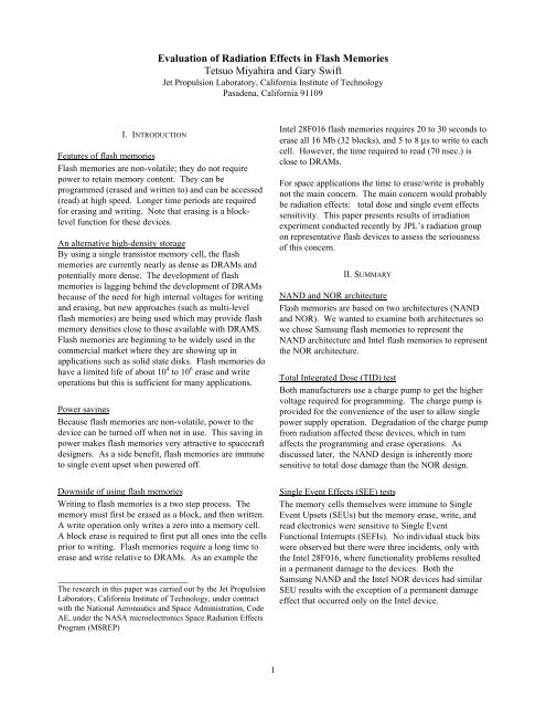
Evaluation of Radiation Effects in Flash Memories Tetsuo Miyahira ...
Evaluation of Radiation Effects in Flash Memories Tetsuo Miyahira ...
Evaluation of Radiation Effects in Flash Memories Tetsuo Miyahira ...

Create successful ePaper yourself
Turn your PDF publications into a flip-book with our unique Google optimized e-Paper software.
I. INTRODUCTION<br />
<strong>Evaluation</strong> <strong>of</strong> <strong>Radiation</strong> <strong>Effects</strong> <strong>in</strong> <strong>Flash</strong> <strong>Memories</strong><br />
<strong>Tetsuo</strong> <strong>Miyahira</strong> and Gary Swift<br />
Jet Propulsion Laboratory, California Institute <strong>of</strong> Technology<br />
Pasadena, California 91109<br />
Features <strong>of</strong> flash memories<br />
<strong>Flash</strong> memories are non-volatile; they do not require<br />
power to reta<strong>in</strong> memory content. They can be<br />
programmed (erased and written to) and can be accessed<br />
(read) at high speed. Longer time periods are required<br />
for eras<strong>in</strong>g and writ<strong>in</strong>g. Note that eras<strong>in</strong>g is a blocklevel<br />
function for these devices.<br />
An alternative high-density storage<br />
By us<strong>in</strong>g a s<strong>in</strong>gle transistor memory cell, the flash<br />
memories are currently nearly as dense as DRAMs and<br />
potentially more dense. The development <strong>of</strong> flash<br />
memories is lagg<strong>in</strong>g beh<strong>in</strong>d the development <strong>of</strong> DRAMs<br />
because <strong>of</strong> the need for high <strong>in</strong>ternal voltages for writ<strong>in</strong>g<br />
and eras<strong>in</strong>g, but new approaches (such as multi-level<br />
flash memories) are be<strong>in</strong>g used which may provide flash<br />
memory densities close to those available with DRAMS.<br />
<strong>Flash</strong> memories are beg<strong>in</strong>n<strong>in</strong>g to be widely used <strong>in</strong> the<br />
commercial market where they are show<strong>in</strong>g up <strong>in</strong><br />
applications such as solid state disks. <strong>Flash</strong> memories do<br />
have a limited life <strong>of</strong> about 10 4 to 10 6 erase and write<br />
operations but this is sufficient for many applications.<br />
Power sav<strong>in</strong>gs<br />
Because flash memories are non-volatile, power to the<br />
device can be turned <strong>of</strong>f when not <strong>in</strong> use. This sav<strong>in</strong>g <strong>in</strong><br />
power makes flash memories very attractive to spacecraft<br />
designers. As a side benefit, flash memories are immune<br />
to s<strong>in</strong>gle event upset when powered <strong>of</strong>f.<br />
Downside <strong>of</strong> us<strong>in</strong>g flash memories<br />
Writ<strong>in</strong>g to flash memories is a two step process. The<br />
memory must first be erased as a block, and then written.<br />
A write operation only writes a zero <strong>in</strong>to a memory cell.<br />
A block erase is required to first put all ones <strong>in</strong>to the cells<br />
prior to writ<strong>in</strong>g. <strong>Flash</strong> memories require a long time to<br />
erase and write relative to DRAMs. As an example the<br />
_____________________________<br />
The research <strong>in</strong> this paper was carried out by the Jet Propulsion<br />
Laboratory, California Institute <strong>of</strong> Technology, under contract<br />
with the National Aeronautics and Space Adm<strong>in</strong>istration, Code<br />
AE, under the NASA microelectronics Space <strong>Radiation</strong> <strong>Effects</strong><br />
Program (MSREP)<br />
1<br />
Intel 28F016 flash memories requires 20 to 30 seconds to<br />
erase all 16 Mb (32 blocks), and 5 to 8 μs to write to each<br />
cell. However, the time required to read (70 nsec.) is<br />
close to DRAMs.<br />
For space applications the time to erase/write is probably<br />
not the ma<strong>in</strong> concern. The ma<strong>in</strong> concern would probably<br />
be radiation effects: total dose and s<strong>in</strong>gle event effects<br />
sensitivity. This paper presents results <strong>of</strong> irradiation<br />
experiment conducted recently by JPL’s radiation group<br />
on representative flash devices to assess the seriousness<br />
<strong>of</strong> this concern.<br />
II. SUMMARY<br />
NAND and NOR architecture<br />
<strong>Flash</strong> memories are based on two architectures (NAND<br />
and NOR). We wanted to exam<strong>in</strong>e both architectures so<br />
we chose Samsung flash memories to represent the<br />
NAND architecture and Intel flash memories to represent<br />
the NOR architecture.<br />
Total Integrated Dose (TID) test<br />
Both manufacturers use a charge pump to get the higher<br />
voltage required for programm<strong>in</strong>g. The charge pump is<br />
provided for the convenience <strong>of</strong> the user to allow s<strong>in</strong>gle<br />
power supply operation. Degradation <strong>of</strong> the charge pump<br />
from radiation affected these devices, which <strong>in</strong> turn<br />
affects the programm<strong>in</strong>g and erase operations. As<br />
discussed later, the NAND design is <strong>in</strong>herently more<br />
sensitive to total dose damage than the NOR design.<br />
S<strong>in</strong>gle Event <strong>Effects</strong> (SEE) tests<br />
The memory cells themselves were immune to S<strong>in</strong>gle<br />
Event Upsets (SEUs) but the memory erase, write, and<br />
read electronics were sensitive to S<strong>in</strong>gle Event<br />
Functional Interrupts (SEFIs). No <strong>in</strong>dividual stuck bits<br />
were observed but there were three <strong>in</strong>cidents, only with<br />
the Intel 28F016, where functionality problems resulted<br />
<strong>in</strong> a permanent damage to the devices. Both the<br />
Samsung NAND and the Intel NOR devices had similar<br />
SEU results with the exception <strong>of</strong> a permanent damage<br />
effect that occurred only on the Intel device.
III. NAND and NOR architecture<br />
The diagram entitled “NAND and NOR Architecture”<br />
contrasts the basic cell structure <strong>of</strong> both the Samsung<br />
NAND and the Intel NOR flash memories. The cell<br />
structure is very similar to a MOS transistor except for<br />
the float<strong>in</strong>g gate. By add<strong>in</strong>g or remov<strong>in</strong>g charge on this<br />
float<strong>in</strong>g gate one can turn on or <strong>of</strong>f the transistor. A<br />
positive charge on the float<strong>in</strong>g gate relative to the source<br />
turns on the device and a negative charge turns it <strong>of</strong>f.<br />
Because the float<strong>in</strong>g gate is electrically isolated, it reta<strong>in</strong>s<br />
its charge <strong>in</strong>def<strong>in</strong>itely and hence the cell’s non-volatility.<br />
For both the Intel and Samsung devices, eras<strong>in</strong>g is done<br />
by the mechanism <strong>of</strong> Fowler-Nordheim tunnel<strong>in</strong>g. For<br />
both device types, the control gate is grounded. In the<br />
case <strong>of</strong> the Samsung device, programm<strong>in</strong>g voltage is<br />
applied to the substrate, but for the Intel device,<br />
programm<strong>in</strong>g voltage is applied to the source. The<br />
electric field generated causes electrons to tunnel away<br />
from the float<strong>in</strong>g gate mak<strong>in</strong>g it more positive and<br />
turn<strong>in</strong>g the transistor on.<br />
Samsung devices also use a form <strong>of</strong> tunnel<strong>in</strong>g for writ<strong>in</strong>g<br />
<strong>of</strong> <strong>in</strong>dividual float<strong>in</strong>g gates. For writ<strong>in</strong>g, the P-well and<br />
the N-Substrate are grounded and programm<strong>in</strong>g voltage<br />
is applied to the control gate. The voltage on the control<br />
gate is capacitively coupled to the float<strong>in</strong>g gate, which<br />
creates an electric field that causes electrons to tunnel<br />
from the P-well to the float<strong>in</strong>g gate mak<strong>in</strong>g it more<br />
negative turn<strong>in</strong>g <strong>of</strong>f the transistor.<br />
For Intel devices, Channel Hot Electron (CHE) <strong>in</strong>jection<br />
is used to program <strong>in</strong>dividual transistors. For this<br />
approach the source is grounded; the control gate has<br />
programm<strong>in</strong>g voltage (Vpp) applied to it while the dra<strong>in</strong><br />
gets approximately half <strong>of</strong> the programm<strong>in</strong>g voltage<br />
applied to it. The voltage on the control gate is<br />
capacitively coupled to the float<strong>in</strong>g gate. This turns the<br />
transistor on and causes the current (electrons) to flow<br />
from the source to dra<strong>in</strong>. Some <strong>of</strong> these electrons will<br />
have sufficient energy (~3.1eV) to pass through the oxide<br />
charg<strong>in</strong>g the float<strong>in</strong>g gate. Electrons deposited on the<br />
float<strong>in</strong>g gate charge the gate negatively and turns <strong>of</strong>f the<br />
transistor.<br />
Both manufacturers use charge pumps to get the higher<br />
voltages required to program (erase and write) the<br />
memory cells. As mentioned earlier, the charge pump is<br />
sensitive to radiation damage. The Intel 28F016 devices<br />
allow programm<strong>in</strong>g to be done with or without the<br />
charge pump. In the latter case, programm<strong>in</strong>g voltage is<br />
applied us<strong>in</strong>g an external supply. This flexibility allowed<br />
us to evaluate the radiation tolerance <strong>of</strong> the charge pump<br />
by contrast<strong>in</strong>g both options: us<strong>in</strong>g the charge pump and<br />
bypass<strong>in</strong>g the charge pump. Unfortunately, Intel has<br />
2<br />
elim<strong>in</strong>ated the option <strong>of</strong> externally supply<strong>in</strong>g<br />
programm<strong>in</strong>g power <strong>in</strong> its higher density (32 Mb or<br />
greater) parts.<br />
As <strong>in</strong> any MOS device, trapped charge <strong>in</strong> the oxide will<br />
cause a shift <strong>in</strong> the threshold voltage. The trapped<br />
charge from erase and write operations limits the number<br />
<strong>of</strong> erase/write operations allowable by these devices. The<br />
additional effect <strong>of</strong> trapped charges from ioniz<strong>in</strong>g<br />
radiation will also cause the device to fail. To date there<br />
is little data on the comb<strong>in</strong>ed effect <strong>of</strong> the two failure<br />
mechanisms.<br />
The NAND architecture typically uses eight or sixteen<br />
cells that are stacked <strong>in</strong> series with a common bit l<strong>in</strong>e.<br />
While this arrangement allows for a more compact<br />
design, it does cause the device to be more sensitive to<br />
radiation damage s<strong>in</strong>ce radiation-<strong>in</strong>duced leakage will<br />
add together.<br />
IV. TID RESULTS<br />
TID failure <strong>of</strong> Intel and Samsung flash memories<br />
The data displayed <strong>in</strong> chart entitled “Total Dose Failure<br />
Levels” is the result <strong>of</strong> test<strong>in</strong>g on six test devices from the<br />
two manufacturers. The devices were irradiated with<br />
Co 60 at room temperature at a rate <strong>of</strong> 25 rads/sec. The<br />
devices were statically biased with both Vpp and Vdd at<br />
5V.<br />
As this graph <strong>in</strong>dicates, the Intel NOR flash memory did<br />
not fail until 100 krad(Si) when tested bypass<strong>in</strong>g the<br />
<strong>in</strong>ternal charge pump. An external supply was used to<br />
supply programm<strong>in</strong>g voltage for this mode. However<br />
when the Intel device was tested us<strong>in</strong>g the <strong>in</strong>ternal<br />
charge pump, they failed at ~24 krads. The Samsung<br />
NAND flash memory which had no provision for<br />
bypass<strong>in</strong>g the charge pump failed at ~10 krads. Based on<br />
the results from the Intel tests, with and without the<br />
charge pump, it is clear that the charge pump has a<br />
significant effect on radiation hardness. The data also<br />
suggest that the NAND architecture is more susceptible<br />
to TID damage than the NOR architecture.<br />
Time to erase us<strong>in</strong>g <strong>in</strong>ternal charge pump vs. us<strong>in</strong>g<br />
external supply<br />
The plot entitled “Time Required to Erase only” <strong>in</strong>cludes<br />
data from Intel devices because Samsung devices had no<br />
provisions for bypass<strong>in</strong>g the charge pump. When the<br />
Intel flash memories were tested with the charge pump<br />
bypassed, the data showed no degradation <strong>in</strong> erase time<br />
up to 30 krad(Si). When the <strong>in</strong>ternal charge pump was<br />
used, the time to erase <strong>in</strong>creased from 30 seconds at pre-
irradiation to 143 seconds at 12 krads for the worst <strong>of</strong> the<br />
six test devices.<br />
Supply current (Idd) degradation<br />
In the plot entitled “Supply Current (Idd)” shows that Idd<br />
for the Samsung device began to rise rapidly at about 8<br />
krads and the device failed functionally at about ~10<br />
krads. Idd for the Intel device began to rise rapidly at<br />
about 20 krads and the device failed functionally at<br />
~24 krads.<br />
V. SEU RESULTS<br />
SEU Tests<br />
Unpowered mode. The purpose <strong>of</strong> this test was to<br />
determ<strong>in</strong>e if the float<strong>in</strong>g gate would upset with heavy<br />
ions. <strong>Flash</strong> memories use an embedded microcontroller<br />
to improve erase/write times. The device was left<br />
unpowered, dur<strong>in</strong>g irradiation, to prevent upsets <strong>in</strong> the<br />
microcontroller, which <strong>in</strong> turn could cause an upsets <strong>in</strong><br />
the memory cells. The memory was loaded with a known<br />
pattern prior to the test and left unpowered while be<strong>in</strong>g<br />
irradiated with heavy ions. After the irradiation, the<br />
device was powered and tested to see if there were any<br />
changes to the pattern. No cell upset occurred when<br />
tested <strong>in</strong> this mode even up to an effective LET <strong>of</strong> 120<br />
MeV-cm 2 /mg.<br />
Static mode. For this mode, the flash memory was<br />
powered but there was no active address<strong>in</strong>g tak<strong>in</strong>g place<br />
dur<strong>in</strong>g irradiation. Most <strong>of</strong> the test<strong>in</strong>g was done us<strong>in</strong>g<br />
this mode. Before the irradiation, the device was loaded<br />
with a known pattern and at the completion <strong>of</strong> the<br />
irradiation, the device was tested to see if the memory<br />
content had changed. When test<strong>in</strong>g <strong>in</strong> this mode,<br />
functional <strong>in</strong>terrupts (SEFIs) would occur that <strong>in</strong> most<br />
cases required power cycl<strong>in</strong>g (turn<strong>in</strong>g Vdd <strong>of</strong>f and then on<br />
aga<strong>in</strong>) to clear the error condition. We were able to<br />
identify seven error modes (lockup conditions). Besides<br />
the seven error modes, three Intel devices had<br />
catastrophic high current condition that occurred dur<strong>in</strong>g<br />
functionality test after the irradiation was completed. We<br />
did not experience this catastrophic high current<br />
condition with the Samsung memories.<br />
We had no visibility <strong>of</strong> functionality dur<strong>in</strong>g irradiation,<br />
because we were not address<strong>in</strong>g the test device when<br />
tested <strong>in</strong> the static mode. Each irradiation run therefore<br />
became a pass or fail test. In order to determ<strong>in</strong>e a cross<br />
section, we selected fluence so that some <strong>of</strong> the runs<br />
resulted <strong>in</strong> a SEFI and some did not. Cross section was<br />
determ<strong>in</strong>ed by add<strong>in</strong>g the number <strong>of</strong> SEFIs then divid<strong>in</strong>g<br />
by the total fluence (passes as well as fails). The plot <strong>of</strong><br />
3<br />
the cross section as a function <strong>of</strong> LET for the Intel<br />
28F016SV is shown on the graph entitled “Cross Section<br />
for Complex Functional Upset Modes.” The error bars<br />
are large because we did not know at what po<strong>in</strong>t dur<strong>in</strong>g<br />
the irradiation the SEFI occurred or if more than one<br />
SEFI occurred dur<strong>in</strong>g that run.<br />
Read mode and erase/write mode. Most <strong>of</strong> the time<br />
was spent test<strong>in</strong>g <strong>in</strong> the static mode. The results from<br />
tests <strong>in</strong> read and erase/write modes were too limited to<br />
<strong>in</strong>clude <strong>in</strong> this paper. We will address these modes<br />
further <strong>in</strong> future tests.<br />
Isolat<strong>in</strong>g the memory array<br />
We used a copper shield to mask <strong>of</strong>f the microcontroller.<br />
The diagram entitled “Chip Micrograph” shows the area<br />
that was masked from the heavy ions. This was done to<br />
see if memory upsets would still occur. We got mixed<br />
results from this test, possibly because the sens<strong>in</strong>g and<br />
high voltage circuitry was <strong>in</strong>terspersed with the memory<br />
array, and could not be masked. With the Intel<br />
28F016SA memories, we observed no errors. The<br />
28F016SV (smart voltage) devices, however, did appear<br />
to exhibit memory errors at very high LET. However,<br />
the cross section was very low, and it is likely that the<br />
apparent memory errors are caused by the response <strong>of</strong> the<br />
more complex SV microcontroller. Accord<strong>in</strong>g to the<br />
manufacturer, the SV and SA memory cell technologies<br />
are identical and should have behaved similarly.<br />
VI. PLAN FOR FOLLOW ON TESTS<br />
X2000 Project<br />
X2000 Project is driv<strong>in</strong>g the flash memory survey. There<br />
are currently five missions proposed for X2000 project<br />
(Europa, Pluto, Solar Probe, Champollion, and a Mars<br />
mission). The <strong>Radiation</strong> <strong>Effects</strong> Group at JPL is<br />
primarily concerned with the Europa spacecraft because<br />
<strong>of</strong> its severe radiation environment. The Europa<br />
spacecraft is expected to be exposed to mostly electron<br />
dose <strong>of</strong> about four megarad(Si), beh<strong>in</strong>d 100 mils <strong>of</strong><br />
alum<strong>in</strong>um. Design trade studies <strong>in</strong>dicate that it is<br />
possible to shield to about 40 krad(Si) <strong>in</strong> order to ga<strong>in</strong> the<br />
advantages <strong>of</strong> us<strong>in</strong>g commercial flash and /or DRAMS as<br />
opposed to us<strong>in</strong>g an all radiation hardened SRAM. If we<br />
are able to f<strong>in</strong>d a suitable flash memory, the X2000<br />
modular architecture needs at least one giga-bit and<br />
would like eight giga-bits <strong>of</strong> flash memory for each<br />
spacecraft. The follow-on flash memory evaluation will<br />
be done <strong>in</strong> three steps, as described below.<br />
S<strong>in</strong>gle Event Latchup (SEL) test and cursory S<strong>in</strong>gle<br />
Event Upset (SEU) tests
The first test is planned for first quarter <strong>of</strong> FY99.<br />
(October/November time frame). We are <strong>in</strong> the process<br />
<strong>of</strong> purchas<strong>in</strong>g flash memories from several<br />
manufacturers, <strong>in</strong>clud<strong>in</strong>g denser Samsung and Intel<br />
devices (32 Mb or larger). The Intel devices to be tested<br />
are a new multi-level technology where each transistor<br />
stores two bits.<br />
TID test on most <strong>of</strong> the devices<br />
We plan to test all <strong>of</strong> the devices that were tested for<br />
latchup, unless the SEL data shows a significant reason<br />
to omit the device from the test matrix<br />
Detailed SEU evaluation<br />
We plan to select two devices based on the SEL and TID<br />
test results and perform a detailed SEU evaluation us<strong>in</strong>g<br />
a new test system currently <strong>in</strong> development. A new test<br />
system currently be<strong>in</strong>g developed will be capable <strong>of</strong><br />
captur<strong>in</strong>g detailed <strong>in</strong>formation on each upset and/or SEFI<br />
under s<strong>of</strong>tware control.<br />
New PCI-based test system<br />
The new test system is much faster than the current<br />
system and will allow one to scan through the memory<br />
more quickly and therefore provide a more complete SEU<br />
evaluation. The new system is based on the 33 MHz, 32bit<br />
PCI bus <strong>in</strong>stead <strong>of</strong> the 8 MHz, 16-bit ISA bus, which<br />
the current system uses. It is expected that an order <strong>of</strong><br />
magnitude <strong>in</strong>crease <strong>in</strong> performance will be ga<strong>in</strong>ed.<br />
VII. Conclusions<br />
TID conclusions<br />
• NOR architecture is <strong>in</strong>herently more robust.<br />
• Internal charge pump is particularly susceptible.<br />
• Parameters most sensitive to damage are erase/write<br />
time.<br />
• When the charge pump is bypassed the operat<strong>in</strong>g<br />
current is the most sensitive parameter.<br />
SEL conclusions<br />
• There are enough commercial manufacturers that<br />
some will have SEL immunity.<br />
SEU conclusions<br />
• The memory cells are robust.<br />
• “Smarter” control logic <strong>in</strong>creases SEU error modes<br />
and susceptibility.<br />
• With the exception <strong>of</strong> the catastrophic high current<br />
condition that occurred only with the Intel devices,<br />
4<br />
devices from both manufacturers had similar SEU<br />
results.<br />
Unfortunately COTS is driv<strong>in</strong>g the market towards more<br />
radiation sensitivity.<br />
• External program supply option is be<strong>in</strong>g elim<strong>in</strong>ated.<br />
• Inherently more sensitive NAND architecture is<br />
be<strong>in</strong>g used by more manufacturers.<br />
• Control logic is becom<strong>in</strong>g “smarter” add<strong>in</strong>g more<br />
registers and, thus, SEU susceptibility.<br />
VIII. Acknowledgements<br />
Significant efforts and contributions to this paper by<br />
other (past and present) members <strong>of</strong> JPL’s <strong>Radiation</strong><br />
<strong>Effects</strong> Group are gratefully acknowledged: Larry<br />
Edmonds, Steve Guert<strong>in</strong>, Allan Johnston, Choon Lee,<br />
Don Nichols, Duc Nguyen, Michael O’Connor, Bernie<br />
Rax, Luis Selva, Harvey Schwartz, and Mike Wiedeman.<br />
IX. References<br />
[1] D. N. Nguyen, C. I. Lee, and A. H. Johnston, “Total<br />
Ioniz<strong>in</strong>g Dose <strong>Effects</strong> on <strong>Flash</strong> <strong>Memories</strong>,” 1998 IEEE<br />
<strong>Radiation</strong> <strong>Effects</strong> Data Workshop, p. 100.<br />
[2] H. R. Schwartz and D. K. Nichols, “S<strong>in</strong>gle-Event<br />
Upset <strong>in</strong> <strong>Flash</strong> <strong>Memories</strong>,” IEEE Transactions on<br />
Nuclear Science, Vol. 44, p. 2315.
NAND and NOR Architectures<br />
5