Evaluation of Radiation Effects in Flash Memories Tetsuo Miyahira ...
Evaluation of Radiation Effects in Flash Memories Tetsuo Miyahira ...
Evaluation of Radiation Effects in Flash Memories Tetsuo Miyahira ...

You also want an ePaper? Increase the reach of your titles
YUMPU automatically turns print PDFs into web optimized ePapers that Google loves.
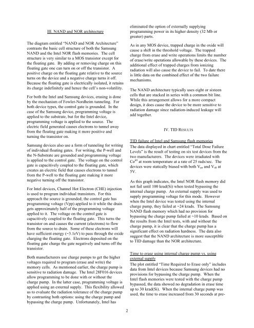
III. NAND and NOR architecture<br />
The diagram entitled “NAND and NOR Architecture”<br />
contrasts the basic cell structure <strong>of</strong> both the Samsung<br />
NAND and the Intel NOR flash memories. The cell<br />
structure is very similar to a MOS transistor except for<br />
the float<strong>in</strong>g gate. By add<strong>in</strong>g or remov<strong>in</strong>g charge on this<br />
float<strong>in</strong>g gate one can turn on or <strong>of</strong>f the transistor. A<br />
positive charge on the float<strong>in</strong>g gate relative to the source<br />
turns on the device and a negative charge turns it <strong>of</strong>f.<br />
Because the float<strong>in</strong>g gate is electrically isolated, it reta<strong>in</strong>s<br />
its charge <strong>in</strong>def<strong>in</strong>itely and hence the cell’s non-volatility.<br />
For both the Intel and Samsung devices, eras<strong>in</strong>g is done<br />
by the mechanism <strong>of</strong> Fowler-Nordheim tunnel<strong>in</strong>g. For<br />
both device types, the control gate is grounded. In the<br />
case <strong>of</strong> the Samsung device, programm<strong>in</strong>g voltage is<br />
applied to the substrate, but for the Intel device,<br />
programm<strong>in</strong>g voltage is applied to the source. The<br />
electric field generated causes electrons to tunnel away<br />
from the float<strong>in</strong>g gate mak<strong>in</strong>g it more positive and<br />
turn<strong>in</strong>g the transistor on.<br />
Samsung devices also use a form <strong>of</strong> tunnel<strong>in</strong>g for writ<strong>in</strong>g<br />
<strong>of</strong> <strong>in</strong>dividual float<strong>in</strong>g gates. For writ<strong>in</strong>g, the P-well and<br />
the N-Substrate are grounded and programm<strong>in</strong>g voltage<br />
is applied to the control gate. The voltage on the control<br />
gate is capacitively coupled to the float<strong>in</strong>g gate, which<br />
creates an electric field that causes electrons to tunnel<br />
from the P-well to the float<strong>in</strong>g gate mak<strong>in</strong>g it more<br />
negative turn<strong>in</strong>g <strong>of</strong>f the transistor.<br />
For Intel devices, Channel Hot Electron (CHE) <strong>in</strong>jection<br />
is used to program <strong>in</strong>dividual transistors. For this<br />
approach the source is grounded; the control gate has<br />
programm<strong>in</strong>g voltage (Vpp) applied to it while the dra<strong>in</strong><br />
gets approximately half <strong>of</strong> the programm<strong>in</strong>g voltage<br />
applied to it. The voltage on the control gate is<br />
capacitively coupled to the float<strong>in</strong>g gate. This turns the<br />
transistor on and causes the current (electrons) to flow<br />
from the source to dra<strong>in</strong>. Some <strong>of</strong> these electrons will<br />
have sufficient energy (~3.1eV) to pass through the oxide<br />
charg<strong>in</strong>g the float<strong>in</strong>g gate. Electrons deposited on the<br />
float<strong>in</strong>g gate charge the gate negatively and turns <strong>of</strong>f the<br />
transistor.<br />
Both manufacturers use charge pumps to get the higher<br />
voltages required to program (erase and write) the<br />
memory cells. As mentioned earlier, the charge pump is<br />
sensitive to radiation damage. The Intel 28F016 devices<br />
allow programm<strong>in</strong>g to be done with or without the<br />
charge pump. In the latter case, programm<strong>in</strong>g voltage is<br />
applied us<strong>in</strong>g an external supply. This flexibility allowed<br />
us to evaluate the radiation tolerance <strong>of</strong> the charge pump<br />
by contrast<strong>in</strong>g both options: us<strong>in</strong>g the charge pump and<br />
bypass<strong>in</strong>g the charge pump. Unfortunately, Intel has<br />
2<br />
elim<strong>in</strong>ated the option <strong>of</strong> externally supply<strong>in</strong>g<br />
programm<strong>in</strong>g power <strong>in</strong> its higher density (32 Mb or<br />
greater) parts.<br />
As <strong>in</strong> any MOS device, trapped charge <strong>in</strong> the oxide will<br />
cause a shift <strong>in</strong> the threshold voltage. The trapped<br />
charge from erase and write operations limits the number<br />
<strong>of</strong> erase/write operations allowable by these devices. The<br />
additional effect <strong>of</strong> trapped charges from ioniz<strong>in</strong>g<br />
radiation will also cause the device to fail. To date there<br />
is little data on the comb<strong>in</strong>ed effect <strong>of</strong> the two failure<br />
mechanisms.<br />
The NAND architecture typically uses eight or sixteen<br />
cells that are stacked <strong>in</strong> series with a common bit l<strong>in</strong>e.<br />
While this arrangement allows for a more compact<br />
design, it does cause the device to be more sensitive to<br />
radiation damage s<strong>in</strong>ce radiation-<strong>in</strong>duced leakage will<br />
add together.<br />
IV. TID RESULTS<br />
TID failure <strong>of</strong> Intel and Samsung flash memories<br />
The data displayed <strong>in</strong> chart entitled “Total Dose Failure<br />
Levels” is the result <strong>of</strong> test<strong>in</strong>g on six test devices from the<br />
two manufacturers. The devices were irradiated with<br />
Co 60 at room temperature at a rate <strong>of</strong> 25 rads/sec. The<br />
devices were statically biased with both Vpp and Vdd at<br />
5V.<br />
As this graph <strong>in</strong>dicates, the Intel NOR flash memory did<br />
not fail until 100 krad(Si) when tested bypass<strong>in</strong>g the<br />
<strong>in</strong>ternal charge pump. An external supply was used to<br />
supply programm<strong>in</strong>g voltage for this mode. However<br />
when the Intel device was tested us<strong>in</strong>g the <strong>in</strong>ternal<br />
charge pump, they failed at ~24 krads. The Samsung<br />
NAND flash memory which had no provision for<br />
bypass<strong>in</strong>g the charge pump failed at ~10 krads. Based on<br />
the results from the Intel tests, with and without the<br />
charge pump, it is clear that the charge pump has a<br />
significant effect on radiation hardness. The data also<br />
suggest that the NAND architecture is more susceptible<br />
to TID damage than the NOR architecture.<br />
Time to erase us<strong>in</strong>g <strong>in</strong>ternal charge pump vs. us<strong>in</strong>g<br />
external supply<br />
The plot entitled “Time Required to Erase only” <strong>in</strong>cludes<br />
data from Intel devices because Samsung devices had no<br />
provisions for bypass<strong>in</strong>g the charge pump. When the<br />
Intel flash memories were tested with the charge pump<br />
bypassed, the data showed no degradation <strong>in</strong> erase time<br />
up to 30 krad(Si). When the <strong>in</strong>ternal charge pump was<br />
used, the time to erase <strong>in</strong>creased from 30 seconds at pre-