online .pdf paper (for personal use only) - Chair of Materials Science ...
online .pdf paper (for personal use only) - Chair of Materials Science ...
online .pdf paper (for personal use only) - Chair of Materials Science ...

Create successful ePaper yourself
Turn your PDF publications into a flip-book with our unique Google optimized e-Paper software.
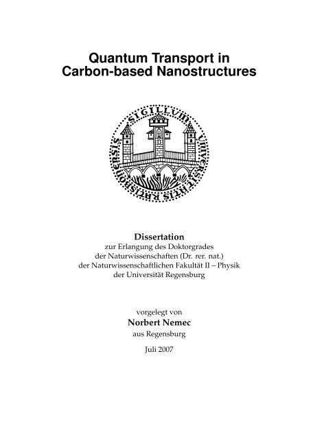
Quantum Transport in<br />
Carbon-based Nanostructures<br />
Dissertation<br />
zur Erlangung des Doktorgrades<br />
der Naturwissenschaften (Dr. rer. nat.)<br />
der Naturwissenschaftlichen Fakultät II – Physik<br />
der Universität Regensburg<br />
vorgelegt von<br />
Norbert Nemec<br />
aus Regensburg<br />
Juli 2007
Die Arbeit wurde angeleitet von:<br />
Pr<strong>of</strong>. Gianaurelio Cuniberti<br />
Gutachter:<br />
Pr<strong>of</strong>. Gianaurelio Cuniberti<br />
Pr<strong>of</strong>. Milena Grifoni
Contents<br />
Introduction 9<br />
1. Carbon-based nanostructures 13<br />
1.1. Hybridization <strong>of</strong> carbon orbitals . . . . . . . . . . . . . . . . . . . . . . . . 14<br />
1.2. Graphite . . . . . . . . . . . . . . . . . . . . . . . . . . . . . . . . . . . . . . 18<br />
1.3. Graphene . . . . . . . . . . . . . . . . . . . . . . . . . . . . . . . . . . . . . . 20<br />
1.3.1. Isolation by exfoliation . . . . . . . . . . . . . . . . . . . . . . . . . . 21<br />
1.3.2. Synthesis by epitaxial growth . . . . . . . . . . . . . . . . . . . . . . 22<br />
1.3.3. Geometry . . . . . . . . . . . . . . . . . . . . . . . . . . . . . . . . . 22<br />
1.4. Graphene nanoribbons . . . . . . . . . . . . . . . . . . . . . . . . . . . . . . 24<br />
1.5. Carbon nanotubes . . . . . . . . . . . . . . . . . . . . . . . . . . . . . . . . . 26<br />
1.5.1. Synthesis methods . . . . . . . . . . . . . . . . . . . . . . . . . . . . 28<br />
1.5.2. Single-wall carbon nanotubes . . . . . . . . . . . . . . . . . . . . . . 30<br />
1.5.3. Multiwall carbon nanotubes . . . . . . . . . . . . . . . . . . . . . . . 32<br />
1.6. Fullerenes . . . . . . . . . . . . . . . . . . . . . . . . . . . . . . . . . . . . . 32<br />
2. Electronic structure 35<br />
2.1. The tight-binding approximation . . . . . . . . . . . . . . . . . . . . . . . . 36<br />
2.1.1. Obtaining a tight-binding Hamiltonian . . . . . . . . . . . . . . . . 37<br />
2.1.2. Single orbital tight-binding approximation <strong>of</strong> graphitic structures . 38<br />
2.1.3. Slater-Koster parameterization <strong>of</strong> carbon structures . . . . . . . . . 40<br />
2.2. Band structure <strong>of</strong> graphene . . . . . . . . . . . . . . . . . . . . . . . . . . . 40<br />
2.2.1. Graphene with full basis set . . . . . . . . . . . . . . . . . . . . . . . 42<br />
2.3. Band structure <strong>of</strong> single-wall carbon nanotubes . . . . . . . . . . . . . . . . 43<br />
2.4. Band structure <strong>of</strong> graphene nanoribbons . . . . . . . . . . . . . . . . . . . . 46<br />
2.5. Beyond tight-binding: Density functional theory . . . . . . . . . . . . . . . 46<br />
3. Theory <strong>of</strong> quantum transport 51<br />
3.1. Mesoscopic length scales . . . . . . . . . . . . . . . . . . . . . . . . . . . . . 52<br />
3.2. The transport regimes . . . . . . . . . . . . . . . . . . . . . . . . . . . . . . 57<br />
3.3. Landauer transport <strong>for</strong>malism . . . . . . . . . . . . . . . . . . . . . . . . . . 58<br />
3.4. The quantum mechanical transmission . . . . . . . . . . . . . . . . . . . . . 59<br />
3.4.1. Transmission through single molecules . . . . . . . . . . . . . . . . 62<br />
3.4.2. Transmission <strong>of</strong> periodic systems . . . . . . . . . . . . . . . . . . . . 63<br />
3.4.3. Systems with periodic leads . . . . . . . . . . . . . . . . . . . . . . . 65<br />
3.4.4. Tunneling contacts . . . . . . . . . . . . . . . . . . . . . . . . . . . . 66<br />
3.4.5. Resonant tunneling and Fabry-Pérot physics . . . . . . . . . . . . . 67<br />
3.4.6. Structureless leads . . . . . . . . . . . . . . . . . . . . . . . . . . . . 69<br />
3.5. Beyond coherent transport: interactions and decoherence . . . . . . . . . . 70<br />
5
Contents<br />
4. Electrical contacts to nanotubes and -ribbons 73<br />
4.1. Conventional contact models . . . . . . . . . . . . . . . . . . . . . . . . . . 74<br />
4.1.1. Carbon nanotube electrodes . . . . . . . . . . . . . . . . . . . . . . . 75<br />
4.1.2. Structureless electrodes . . . . . . . . . . . . . . . . . . . . . . . . . 76<br />
4.1.3. Atomically modeled electrodes . . . . . . . . . . . . . . . . . . . . . 76<br />
4.2. Extended contacts . . . . . . . . . . . . . . . . . . . . . . . . . . . . . . . . . 76<br />
4.2.1. Analytic model . . . . . . . . . . . . . . . . . . . . . . . . . . . . . . 79<br />
4.2.2. Generalization to arbitrary injection energies . . . . . . . . . . . . . 84<br />
4.2.3. Non-diagonal contacts . . . . . . . . . . . . . . . . . . . . . . . . . . 86<br />
4.2.4. Realistic contacts to carbon nanotubes and graphene nanoribbons . 86<br />
4.2.5. Three-terminal setup and Fabry-Pérot physics . . . . . . . . . . . . 89<br />
4.2.6. Non-epitaxial contacts . . . . . . . . . . . . . . . . . . . . . . . . . . 91<br />
4.2.7. Material related calculations . . . . . . . . . . . . . . . . . . . . . . 91<br />
4.3. Ferromagnetic contacts and spin transport . . . . . . . . . . . . . . . . . . . 96<br />
4.3.1. Modeling ferromagnetic leads . . . . . . . . . . . . . . . . . . . . . 97<br />
4.3.2. Magnetoresistance <strong>of</strong> an ordered nanotube . . . . . . . . . . . . . . 99<br />
4.3.3. Effects <strong>of</strong> disorder . . . . . . . . . . . . . . . . . . . . . . . . . . . . 99<br />
5. Disorder and defects 103<br />
5.1. Anderson model <strong>for</strong> disorder . . . . . . . . . . . . . . . . . . . . . . . . . . 105<br />
5.2. The elastic mean free path . . . . . . . . . . . . . . . . . . . . . . . . . . . . 106<br />
5.3. Strong localization . . . . . . . . . . . . . . . . . . . . . . . . . . . . . . . . 109<br />
5.4. Vacancies and defects . . . . . . . . . . . . . . . . . . . . . . . . . . . . . . . 111<br />
5.5. Graphene nanoribbons . . . . . . . . . . . . . . . . . . . . . . . . . . . . . . 114<br />
6. Multilayer graphene and carbon nanotubes 117<br />
6.1. Commensurability . . . . . . . . . . . . . . . . . . . . . . . . . . . . . . . . 118<br />
6.2. Modeling the interlayer coupling . . . . . . . . . . . . . . . . . . . . . . . . 120<br />
6.3. Bilayer graphene . . . . . . . . . . . . . . . . . . . . . . . . . . . . . . . . . 122<br />
6.4. Double-wall carbon nanotubes . . . . . . . . . . . . . . . . . . . . . . . . . 124<br />
6.4.1. Commensurate double-wall tubes . . . . . . . . . . . . . . . . . . . 125<br />
6.4.2. Incommensurate double-wall tubes . . . . . . . . . . . . . . . . . . 127<br />
6.5. Telescopic carbon nanotubes . . . . . . . . . . . . . . . . . . . . . . . . . . . 129<br />
6.5.1. Armchair telescopic tubes . . . . . . . . . . . . . . . . . . . . . . . . 129<br />
6.5.2. Zigzag telescopic tubes . . . . . . . . . . . . . . . . . . . . . . . . . 132<br />
6.5.3. Model <strong>of</strong> telescopic quantum wires . . . . . . . . . . . . . . . . . . 132<br />
7. Magnetoelectronic structure and fractality 137<br />
7.1. Peierls substitution . . . . . . . . . . . . . . . . . . . . . . . . . . . . . . . . 139<br />
7.2. H<strong>of</strong>stadter butterfly . . . . . . . . . . . . . . . . . . . . . . . . . . . . . . . . 140<br />
7.3. Butterfly and anomalous Landau levels <strong>of</strong> graphene . . . . . . . . . . . . . 142<br />
7.4. Butterfly <strong>of</strong> single-wall nanotubes . . . . . . . . . . . . . . . . . . . . . . . 144<br />
7.5. Graphene nanoribbons . . . . . . . . . . . . . . . . . . . . . . . . . . . . . . 147<br />
7.6. Periodic gauge . . . . . . . . . . . . . . . . . . . . . . . . . . . . . . . . . . . 147<br />
7.7. Bilayer graphene . . . . . . . . . . . . . . . . . . . . . . . . . . . . . . . . . 149<br />
7.8. Butterfly <strong>of</strong> double-wall nanotubes . . . . . . . . . . . . . . . . . . . . . . . 151<br />
Conclusions and perspectives 155<br />
Appendices 159<br />
6
Contents<br />
A. Decimation techniques 159<br />
A.1. The fundamental equation <strong>of</strong> decimation . . . . . . . . . . . . . . . . . . . 159<br />
A.1.1. Application to Green functions: Bipartite systems . . . . . . . . . . 160<br />
A.2. Tripartite systems . . . . . . . . . . . . . . . . . . . . . . . . . . . . . . . . . 161<br />
A.3. Finite block tridiagonal systems . . . . . . . . . . . . . . . . . . . . . . . . . 162<br />
A.3.1. Thoughts about efficiency . . . . . . . . . . . . . . . . . . . . . . . . 164<br />
A.4. Periodic systems . . . . . . . . . . . . . . . . . . . . . . . . . . . . . . . . . . 165<br />
A.4.1. Simple iterative scheme . . . . . . . . . . . . . . . . . . . . . . . . . 166<br />
A.4.2. Renormalization-decimation algorithm . . . . . . . . . . . . . . . . 167<br />
A.4.3. Umerski algorithm . . . . . . . . . . . . . . . . . . . . . . . . . . . . 169<br />
B. Analytic derivations 171<br />
B.1. Supersymmetric spectrum <strong>of</strong> graphene . . . . . . . . . . . . . . . . . . . . 171<br />
B.2. The linear-chain model <strong>of</strong> extended contacts . . . . . . . . . . . . . . . . . 174<br />
B.2.1. Transmission calculations . . . . . . . . . . . . . . . . . . . . . . . . 174<br />
B.2.2. Inverse based on Chebyshev polynomials . . . . . . . . . . . . . . . 176<br />
B.2.3. Surface <strong>of</strong> semi-infinite linear chain . . . . . . . . . . . . . . . . . . 177<br />
B.2.4. Transmission <strong>of</strong> the model system . . . . . . . . . . . . . . . . . . . 178<br />
B.3. The elastic mean free path in carbon nanotubes . . . . . . . . . . . . . . . . 179<br />
C. Numerical implementations 183<br />
C.1. Programming language, libraries and tools . . . . . . . . . . . . . . . . . . 183<br />
C.2. Handling <strong>of</strong> physical units . . . . . . . . . . . . . . . . . . . . . . . . . . . . 184<br />
C.3. Constructing chiral carbon nanotubes . . . . . . . . . . . . . . . . . . . . . 185<br />
C.4. Construction <strong>of</strong> a periodic Hamiltonian . . . . . . . . . . . . . . . . . . . . 188<br />
C.5. Tight-binding interlayer Hamiltonian . . . . . . . . . . . . . . . . . . . . . 189<br />
C.6. Decimation <strong>of</strong> a finite block tridiagonal system . . . . . . . . . . . . . . . . 191<br />
C.7. Renormalization decimation algorithm . . . . . . . . . . . . . . . . . . . . 192<br />
C.8. Periodic gauge . . . . . . . . . . . . . . . . . . . . . . . . . . . . . . . . . . . 193<br />
D. Reprints <strong>of</strong> publications 195<br />
Phys. Status Solidi B 243, 179 (2005) . . . . . . . . . . . . . . . . . . . . . . . . . 196<br />
Phys. Rev. Lett. 96, 076802 (2006) . . . . . . . . . . . . . . . . . . . . . . . . . . . 200<br />
Phys. Rev. B 74, 165411 (2006) . . . . . . . . . . . . . . . . . . . . . . . . . . . . . 204<br />
Phys. Rev. B 75, 201404(R) (2007) . . . . . . . . . . . . . . . . . . . . . . . . . . . 217<br />
Bibliography 221<br />
Acknowledgments 239<br />
7
Contents<br />
8
Introduction<br />
Carbon is the most versatile <strong>of</strong> all elements. It is the structural backbone<br />
<strong>of</strong> all organic molecules and thereby <strong>of</strong> life itself. Pure carbon is found in<br />
nature both as diamond, the hardest material known to mankind, crystal<br />
clear and insulating, or graphite, an excellent lubricant, steel black and<br />
conducting, both differing <strong>only</strong> by the arrangement <strong>of</strong> the carbon atoms<br />
in the crystal structure.<br />
Besides these two natural <strong>for</strong>ms, a whole new class <strong>of</strong> artificial pure<br />
carbon materials has been discovered over the past twenty years: small<br />
spherical molecules called fullerenes (1985), tubular fibers called carbon<br />
nanotubes (1991), monoatomic sheets called graphene (2005), and many<br />
more structures <strong>of</strong> various geometric shapes at a scale <strong>of</strong> nanometers.<br />
The physical properties <strong>of</strong> these materials are promising: fibers stronger<br />
and lighter than steel, Kevlar or spider silk, electrical conductors better<br />
than silver or copper, semiconductors with a tunable band gap. These and<br />
many more visions have been realized and demonstrated in the laboratory<br />
and are about to enter the market.<br />
This development would have been impossible without the progress<br />
that was made in parallel in directly observing and manipulating nanoscale<br />
structures with atomic precision. Complex electronic devices can be<br />
built using single carbon nanotubes and individual molecules, measuring<br />
currents electron by electron.<br />
The technological interest in miniaturization has continued unbroken<br />
<strong>for</strong> decades. Electronic circuits are becoming smaller, faster, cheaper<br />
and more energy efficient at constant rate. Currently, the semiconductor<br />
industry is preparing to start mass production in 45 nm technology. The<br />
roadmap <strong>for</strong> submicroelectronic device fabrication is already laid out<br />
until 2018, when the individual devices on a computer chip are expected<br />
to reach a size <strong>of</strong> 16 nm. This would correspond to a width <strong>of</strong> just about<br />
60 silicon atoms.<br />
It is unclear how long silicon will actually be the adequate material<br />
to keep up with this trend. The precision in production, the long-term<br />
stability, the need <strong>for</strong> chemical doping and finally the laws <strong>of</strong> quantum<br />
9
Introduction<br />
mechanics itself are all factors that are likely to present a hard wall to the<br />
ongoing trend <strong>of</strong> miniaturization.<br />
Carbon nanotubes can be produced reliably at a thickness <strong>of</strong> less than<br />
1 nm, are thermally stable up to 2800 ◦ C, can be either metallic or semiconducting<br />
depending on their structure alone, without need <strong>for</strong> chemical<br />
modification and their quantum electronic properties are well defined.<br />
However, the technological importance <strong>of</strong> carbon nanostructures goes<br />
beyond that <strong>of</strong> a new material <strong>for</strong> building traditional devices. Intrinsically<br />
new concepts have been proved: Electromechanical nanomachines<br />
and chemical sensors have been built from carbon nanotubes, and the<br />
extremely long spin coherence make nanotubes a prominent candidate<br />
<strong>for</strong> spintronic applications.<br />
Graphene is a very recent addition to the family <strong>of</strong> available carbon<br />
nanomaterials, carrying perhaps even more technological potential than<br />
carbon nanotubes. As a flat sheet, graphene holds the promise <strong>of</strong> allowing<br />
the lithographic production <strong>of</strong> complex structures. Its spin coherence is<br />
equally excellent as in nanotubes. Its unique electronic structure is so<br />
fundamentally different from anything that was known be<strong>for</strong>e, that many<br />
<strong>of</strong> implications may not even have been considered yet.<br />
This thesis presents our results <strong>of</strong> the investigation <strong>of</strong> several core issues<br />
<strong>of</strong> quantum transport properties and electronic structure <strong>of</strong> carbon<br />
nanostructures, namely, carbon nanotubes and graphene, based on the<br />
<strong>use</strong> <strong>of</strong> numerical and analytical tools. The understanding <strong>of</strong> electrical<br />
contacts is <strong>of</strong> immediate importance to any experimental ef<strong>for</strong>t in optimizing<br />
charge injection. Defects and disorder are crucial ingredients in<br />
any attempt to capture physical reality in a theoretical model. The interlayer<br />
coupling in multilayer structures has been a field <strong>of</strong> hot debate<br />
<strong>for</strong> several years among experimentalists as well as theoreticians and the<br />
magnetoelectronic structure, closely linked to the anomalous quantum<br />
Hall effect observed in graphene, is one <strong>of</strong> the best examples demonstrating<br />
the extraordinary electronic properties <strong>of</strong> these novel materials.<br />
The outline <strong>of</strong> this thesis is organized as follows:<br />
Chap. 1: Carbon materials A general introduction <strong>of</strong> basic carbon<br />
nanostructures is given, including a brief sketch <strong>of</strong> the history<br />
<strong>of</strong> their discoveries and the most important methods <strong>of</strong> production.<br />
Chap. 2: Electronic structure The models <strong>of</strong> electronic structure are<br />
introduced and the most general electronic properties <strong>of</strong> sp 2 -<br />
hybridized carbon structures derived from them.<br />
10
Chap. 3: Quantum transport The theory <strong>of</strong> coherent quantum transport<br />
in mesoscopic systems is introduced. An overview <strong>of</strong> the various<br />
mesoscopic length scales and their competition in different regimes<br />
<strong>of</strong> transport is given. The Landauer theory <strong>of</strong> coherent quantum<br />
transport is derived and demonstrated on a number <strong>of</strong> characteristic<br />
model cases that display many <strong>of</strong> the core features also present in<br />
carbon nanostructures.<br />
Chap. 4: Contacts A model <strong>for</strong> realistic contacts to a carbon nanotube<br />
in a typical experimental transport measurement setup is studied in<br />
detail. A very general dependency is found between contact length,<br />
coupling strength and contact transparency. The result is demonstrated<br />
to be qualitatively robust against various kinds <strong>of</strong> disorder<br />
and independent <strong>of</strong> details <strong>of</strong> the modeling. The quantitative result<br />
is combined with the results from ab initio calculations to derive<br />
clear predictions <strong>for</strong> experiment.<br />
Chap. 5: Disorder and defects The regimes <strong>of</strong> diffusive transport and<br />
strong localization are studied <strong>for</strong> carbon nanotubes and graphene<br />
nanoribbons with homogeneous model disorder or randomly<br />
distributed point defects. The elastic mean free path and the localization<br />
length are derived perturbatively and compared with the<br />
numerical results.<br />
Chap. 6: Multilayer structures Commensurate and incommensurate<br />
double-wall nanotubes and graphene bilayers are investigated.<br />
The bipartite systems are demonstrated to be determined by approximate<br />
symmetries if the interlayer coupling is chosen smooth<br />
enough. Telescopic nanotubes are studied <strong>for</strong> their resonant transport<br />
properties. A minimal model is solved and <strong>use</strong>d to explain the<br />
resonances.<br />
Chap. 7: Magnetoelectronics The electronic structure <strong>of</strong> carbon nanostructures<br />
in external magnetic fields is computed nonperturbatively<br />
and visualized in H<strong>of</strong>stadter butterfly plots. A periodic gauge<br />
is developed that allows the handling <strong>of</strong> graphene bilayers at arbitrary<br />
relative positions. The general structure <strong>of</strong> the butterfly plots<br />
is discussed and the anomalous Landau level structure <strong>of</strong> graphene<br />
is analyzed <strong>for</strong> graphene bilayers and double-wall nanotubes.<br />
11
Introduction<br />
Part <strong>of</strong> the work presented in this thesis has already been published in<br />
the following international journal articles (see reprints in App. D):<br />
[1] Spin transport in disordered single-wall carbon nanotubes contacted to<br />
ferromagnetic leads, S. Krompiewski, N. Nemec, and G. Cuniberti [Phys.<br />
Status Solidi B 243, 179 (2006)]<br />
[2] Contact Dependence <strong>of</strong> Carrier Injection in Carbon Nanotubes:<br />
An Ab Initio Study, N. Nemec, D. Tománek, and G. Cuniberti [Phys. Rev.<br />
Lett. 96, 076802 (2006)]<br />
[3] H<strong>of</strong>stadter butterflies <strong>of</strong> carbon nanotubes: Pseud<strong>of</strong>ractality<br />
<strong>of</strong> the magnetoelectronic spectrum,<br />
N. Nemec and G. Cuniberti [Phys. Rev. B 74, 165411 (2006)]<br />
[4] H<strong>of</strong>stadter Butterflies <strong>of</strong> Bilayer Graphene,<br />
N. Nemec and G. Cuniberti [Phys. Rev. B 75, 201404 (2007)]<br />
Part <strong>of</strong> the work presented in Sec. 6.5 <strong>of</strong> this thesis has been included<br />
in the diploma thesis by D. Darau [5].<br />
12
Chapter 1.<br />
Carbon-based nanostructures<br />
Carbon occupies a special position in the periodic table <strong>of</strong> chemical elements.<br />
Due to the ability <strong>of</strong> each carbon atom to <strong>for</strong>m up to four strong<br />
covalent bonds to neighboring atoms, carbon can build up a huge variety<br />
<strong>of</strong> complex networks <strong>for</strong>ming the structural backbone <strong>of</strong> the infinite<br />
variety <strong>of</strong> organic molecules which are the material building blocks <strong>of</strong><br />
life itself. All <strong>of</strong> these organic molecules have in common that additional<br />
chemical ingredients (most comm<strong>only</strong> hydrogen and oxygen) are<br />
necessary to terminate the carbon network and to stabilize the molecule.<br />
For a long time, it was believed that the list <strong>of</strong> pure carbon structures<br />
was restricted to the two crystalline modifications diamond and graphite.<br />
Only with the discovery <strong>of</strong> fullerenes in 1985 [149], it became clear<br />
that pure carbon itself also has the potential to <strong>for</strong>m alternative stable<br />
structures and with the identification <strong>of</strong> carbon nanotubes in 1991 [123],<br />
the list <strong>of</strong> observed and proposed carbon nanostructures began to grow<br />
at high pace, soon including single- and double- and multiwall tubes,<br />
multiwall fullerenes, horns, foam and many others. One <strong>of</strong> the most recent<br />
additions to this list was given by the successful isolation <strong>of</strong> single<br />
sheets <strong>of</strong> graphene [194], completing the set <strong>of</strong> zero-, one-, two and three<br />
dimensional crystal structures <strong>of</strong> pure carbon.<br />
Without doubt, the general rise <strong>of</strong> nanotechnology was mainly initiated<br />
by the development <strong>of</strong> imaging and manipulation techniques that allow<br />
us today to clearly observe and even directly act on structures at atomic<br />
scales. With optical microscopy, the wave length <strong>of</strong> light strictly limits<br />
the possible resolution to more than a hundred nanometers. Scanning or<br />
tunneling electron microscopy (SEM/TEM) in principle allows to break<br />
this barrier, but with charged particles, the possibilities <strong>for</strong> observation<br />
are rather limited. Only with the development <strong>of</strong> the scanning tunneling<br />
microscope (STM) by G. Binnig and H. Rohrer in 1981 [35] it became<br />
possible to non-destructively observe structures down to the level <strong>of</strong><br />
single atoms. With the atomic <strong>for</strong>ce microscope (AFM) introduced 1986 by<br />
13
Chapter 1. Carbon-based nanostructures<br />
Figure 1.1.: The shape <strong>of</strong> the relevant orbitals <strong>of</strong> Carbon in their real,<br />
unhybridized <strong>for</strong>m. Displayed are the isosurfaces at positive and negative<br />
sign. (Images taken from Ref. [69])<br />
the same team [34] the direct manipulation <strong>of</strong> such structures also became<br />
possible. With these tools at hand, processes at a scale that had be<strong>for</strong>e been<br />
accessible <strong>only</strong> through indirect methods, could be controlled and studied<br />
with growing precision. This allowed the individual identification and<br />
exploration <strong>of</strong> a great variety <strong>of</strong> pure carbon structures, that would have<br />
been impossible to discern using traditional methods.<br />
In this chapter, we will review the various structures <strong>for</strong>med from pure<br />
sp 2 -hybridized carbon and the basic results about their electronic structure<br />
that will be <strong>use</strong>d throughout this thesis.<br />
1.1. Hybridization <strong>of</strong> carbon orbitals<br />
Carbon (chemical symbol C) has the atomic number 6. Two <strong>of</strong> its electrons<br />
are in the 1s orbital as core electrons. The remaining four electrons reside<br />
in the 2s and 2p orbitals and are available to <strong>for</strong>m chemical bonds. As<br />
the two 2s orbitals are energetically slightly lower then the 2p orbitals, the<br />
<strong>for</strong>mer are filled in the ground state by two electrons, while the other two<br />
electrons reside in 2p orbitals. The energy difference, however, is small<br />
enough, that both sets <strong>of</strong> orbitals can easily <strong>for</strong>m hybrid bonds in various<br />
ways:<br />
The electronic wave function <strong>of</strong> an atom is typically derived as eigenstates<br />
<strong>of</strong> the angular momentum operator in one selected orientation, say,<br />
the z direction. In spherical coordinates, these can be expressed as:<br />
rϑϕ|1s = f1s (r)<br />
rϑϕ|2s = f2s (r)<br />
rϑϕ|2p 0 = f2p (r) sin ϑ<br />
rϑϕ|2p ±1 = f2p (r) cos ϑe ±iϕ<br />
14
1.1. Hybridization <strong>of</strong> carbon orbitals<br />
Figure 1.2.: The three hybridized <strong>for</strong>ms <strong>of</strong> carbon in chemical compounds:<br />
sp hybridization occurs <strong>only</strong> in some typically rather reactive organic compounds,<br />
the alkynes. sp 2 hybridization leads to planar structures like graphite<br />
layers, sp 3 -hybridized carbon atoms <strong>for</strong>m sterical structures like the diamond<br />
crystal. (Images taken from Ref. [69])<br />
where the radial functions f are known analytically <strong>for</strong> the hydrogen<br />
atom, involving the Laguerre polynomials. For atoms with several electrons,<br />
they are qualitatively the same, but the actual shape is known <strong>only</strong><br />
approximately.<br />
As the 2p orbitals are energetically degenerate, they can be linearly<br />
combined in a different way, yielding purely real wave functions:<br />
<br />
2px =<br />
<br />
2py =<br />
<br />
2pz = 2p 0 <br />
1 <br />
√ 2p +1<br />
2<br />
+ −1<br />
2p <br />
i <br />
√ 2p +1<br />
2<br />
− −1<br />
2p <br />
These three orbitals have the identical geometrical shape in three different<br />
orientations. See Fig. 1.1 <strong>for</strong> their comm<strong>only</strong> known visualization.<br />
15
Chapter 1. Carbon-based nanostructures<br />
When <strong>for</strong>ming chemical bonds, carbon is not limited to these atomic<br />
energy eigenstates but tends to merge the energetically close 2s and 2p orbitals,<br />
<strong>for</strong>ming linear combinations in various ways:<br />
16<br />
• Hybridizing the 2s with one 2p orbital gives a set <strong>of</strong> two sp orbitals<br />
in diametrically opposed directions:<br />
<br />
2spa =<br />
<br />
2spb =<br />
1 <br />
√ |2s〉 + 2py<br />
2<br />
1 <br />
√ |2s〉 − 2py<br />
2<br />
Though relevant in organic molecules, this hybridization is not<br />
prevalent in pure carbon structures.<br />
• Far more relevant is the hybridization <strong>of</strong> the 2s orbital with two different<br />
2p orbitals resulting in three equivalent sp 2 orbitals arranged<br />
in plane at an angle <strong>of</strong> 120 ◦ :<br />
<br />
2<br />
2spa =<br />
<br />
2<br />
2spb =<br />
<br />
2<br />
2spc =<br />
1<br />
√ <br />
√ 2 |2s〉 + 2 2px<br />
6<br />
<br />
1<br />
√ √ <br />
√ 2 |2s〉 − 2px + 3 2py<br />
6<br />
<br />
1<br />
√ √ <br />
√ 2 |2s〉 − 2px − 3 2py<br />
6<br />
<br />
These orbitals are capable <strong>of</strong> <strong>for</strong>ming strong covalent bonds with<br />
other carbon atoms resulting in planar structures. The remaining,<br />
unhybridized pz orbital is perpendicular to the plane and may join<br />
with parallel pz orbitals <strong>of</strong> neighboring atoms, <strong>for</strong>ming a strongly<br />
delocalized π orbital that is responsible <strong>for</strong> the electronic properties<br />
<strong>of</strong> the resulting structures. By convention, this remaining atomic<br />
orbital in an sp 2 -hybridized carbon structure is itself referred to as<br />
π orbital.<br />
• Finally, a hybridization <strong>of</strong> the 2s with all three 2p orbitals is also possible,<br />
yielding four equivalent sp 3 orbitals, oriented in a tetrahedral
1.1. Hybridization <strong>of</strong> carbon orbitals<br />
arrangement at an angle <strong>of</strong> ∼ 109 ◦ (tetrahedral angle):<br />
<br />
3<br />
2spa =<br />
<br />
3<br />
2spb =<br />
<br />
3<br />
2spc =<br />
<br />
3<br />
2spd =<br />
1<br />
√ √ <br />
√ 3 |2s〉 + 9 2pz<br />
12<br />
<br />
1<br />
√ √ √ <br />
√ 3 |2s〉 − 1 2pz + 8 2px<br />
12<br />
<br />
1<br />
√ √ √ √ <br />
√ 3 |2s〉 − 1 2pz − 2 2px + 6 2py<br />
12<br />
<br />
1<br />
√ √ √ √ <br />
√ 3 |2s〉 − 1 2pz − 2 2px − 6 2py<br />
12<br />
<br />
These orbitals <strong>for</strong>m strong covalent bonds with neighboring atoms<br />
but are electronically inactive due to their low energy.<br />
Pure-carbon materials can be classified in two major groups given by the<br />
hybridization: diamond is a tetrahedral structure with each atom bound<br />
via four equivalent sp 3 orbitals <strong>for</strong>ming σ-bonds with its neighbors. Generally,<br />
this kind <strong>of</strong> bond leads to an extremely stiff geometry and a large<br />
gap between valence and conduction electrons. Thus, diamond is hard,<br />
transparent and insulating.<br />
Graphite, on the other hand, has a layer structure. Each layer is a monoatomic<br />
sheet <strong>of</strong> carbon atoms arranged in a honeycomb structure. Each<br />
atom has three in-plane neighbors to which it <strong>for</strong>ms equivalent σ-bonds<br />
via sp 2 -hybridized orbitals. The remaining π orbital is free to combine<br />
with those <strong>of</strong> all other atoms into a completely delocalized π band similar<br />
to the delocalized orbital known from aromatic molecules. The layers are<br />
held together by weak van der Waals <strong>for</strong>ces allowing them to slide against<br />
each other with minimal friction.<br />
A single layer graphitic structure is called graphene. Beginning at its<br />
two-dimensional structure it is possible to derive the geometry <strong>of</strong> a whole<br />
family <strong>of</strong> materials. (See Fig. 1.3).<br />
The in-plane σ-bonds <strong>of</strong> sp 2 -hybridized carbon are stiff against longitudinal<br />
<strong>for</strong>ces but s<strong>of</strong>t <strong>for</strong> angular de<strong>for</strong>mations. In a single layer <strong>of</strong> graphene<br />
this is the ca<strong>use</strong> <strong>for</strong> the observed rippling [179]. More generally, this<br />
flexibility opens the door <strong>for</strong> the large range <strong>of</strong> stable graphitic nanostructures.<br />
The electronic properties <strong>of</strong> sp 2 -hybridized carbon materials<br />
are generally determined by the delocalized π orbital. Unlike the strongly<br />
bonding σ orbitals, the π orbitals are generally near to the Fermi energy,<br />
leading to the conducting or semiconducting properties <strong>of</strong> graphitic materials<br />
and opening the path to a wealth <strong>of</strong> potential applications in future<br />
nanoelectronics.<br />
17
Chapter 1. Carbon-based nanostructures<br />
Figure 1.3.: Theoretical construction <strong>of</strong> various carbon structures. Starting<br />
from planar graphene in two dimensions, it can be rolled up to quasizero-dimensional<br />
fullerenes or quasi-one-dimensional nanotubes. Stacks<br />
<strong>of</strong> graphene sheets are graphite. (Image taken from Ref. [93])<br />
1.2. Graphite<br />
Graphite is the chemically most stable allotrope <strong>of</strong> pure carbon. It is found<br />
in nature as a polycrystal with fairly small grains up to a few micrometers.<br />
It is mechanically very s<strong>of</strong>t and electrically conducting. Single crystals<br />
have a highly anisotropic conductivity due to its layer structure: the inplane<br />
conductivity is much larger than the conductivity perpendicular<br />
to the layers. Individual layers slide easily against each other, making<br />
graphene an excellent, technologically important lubricant. Though it is,<br />
in principle, the purest <strong>for</strong>m <strong>of</strong> coal, it is hard to ignite and is there<strong>for</strong>e<br />
not usually <strong>use</strong>d as an energy source.<br />
18
Geometry<br />
1.2. Graphite<br />
Figure 1.4.: Natural graphite (image<br />
originates from “Minerals in Your World”<br />
project, a cooperative ef<strong>for</strong>t between the<br />
United States Geological Survey and the<br />
Mineral In<strong>for</strong>mation Institute)<br />
The first description <strong>of</strong> the hexagonal, layered crystal structure <strong>of</strong> graphene<br />
was given by A. W. Hull in 1917 [121], based on x-ray diffraction. Few<br />
years later, J. D. Bernal could identify the individual planar layers [30],<br />
completing the picture that we have today. Graphite consists <strong>of</strong> parallel<br />
graphene sheets spaced by dinterlayer = 3.34 Å, stacked in an alternative<br />
series (ABAB, comm<strong>only</strong> called Bernal stacking, see Fig. 1.5).<br />
Figure 1.5.: Structure <strong>of</strong> natural graphite (Bernal stacking): Two layers<br />
repeat in alternating positions A and B. One half <strong>of</strong> the atoms are aligned<br />
on top <strong>of</strong> each other, the other half is aligned with the plaquette centers <strong>of</strong><br />
the neighboring layers.<br />
A modification <strong>of</strong> this structure is rhombohedral graphite with the stacking<br />
order ABCABC. It has been shown that natural graphite <strong>of</strong>ten contains a<br />
certain amount in rhombohedral stacking, so, even though this <strong>for</strong>m has<br />
never been isolated, it still has inspired a number <strong>of</strong> theoretical works [106,<br />
19
Chapter 1. Carbon-based nanostructures<br />
Figure 1.6.: STM (left) and AFM (right) image <strong>of</strong> a graphite surface. While<br />
the AFM images each atom equally, the STM is sensitive to whether an<br />
atom is on top <strong>of</strong> another atom or a hole in the second layer. This way, the<br />
Bernal stacking <strong>of</strong> the top two layers is indirectly confirmed. (Image taken<br />
from Ref. [115])<br />
47, 57], especially as an intermediate state in the transition from graphite<br />
to diamond [139, 84].<br />
A further modification is turbostratic graphite where the individual layers<br />
are rotated by random angles against each other. Such structures<br />
arise from mechanical de<strong>for</strong>mation <strong>of</strong> graphite. In this case, the crystalline<br />
nature <strong>of</strong> graphite is lost and quasi-crystalline properties are to be<br />
expected.<br />
1.3. Graphene<br />
Single layer graphene—the latest addition to the family <strong>of</strong> experimentally<br />
realized carbon nanomaterials [194]—is actually the most basic building<br />
block <strong>for</strong> the theoretical understanding <strong>of</strong> all other sp 2 -hybridized carbon<br />
structures: graphite, as a stack <strong>of</strong> graphene sheets, or nanotubes and<br />
fullerenes as rolled-up graphene. Two-dimensional crystals were long<br />
believed not to exist in nature, based on theoretical reasoning saying that<br />
quantum mechanical length fluctuation <strong>of</strong> individual bonds would add<br />
up logarithmically over distance, destroying the long-range order that<br />
defines a crystal [211, 178]. In fact, however, freely suspended graphene<br />
layers do exist [179, 180], and it is now widely believed that the observed<br />
fluctuations in the third dimensions help in stabilizing the structure. An<br />
alternative conjecture would, <strong>of</strong> course, be that the theoretical veto simply<br />
may not apply <strong>for</strong> finite size patches.<br />
20
1.3.1. Isolation by exfoliation<br />
1.3. Graphene<br />
Figure 1.7.: SEM image <strong>of</strong> a graphene<br />
flake deposited on a SiO2 substrate.<br />
The three shades <strong>of</strong> gray show<br />
sections <strong>of</strong> mono-, bi- and trilayer<br />
graphene. (Courtesy <strong>of</strong> U. Stöberl,<br />
Uni Regensburg)<br />
Considering the general desire to isolate single layers <strong>of</strong> graphene, it is<br />
surprising how long it took be<strong>for</strong>e the first success and even more surprising,<br />
considering the simple approach that finally led to success: using<br />
scotch tape to repeatedly peel <strong>of</strong>f flakes from pyrolytic graphite that become<br />
thinner with each step until finally, there is a single layer left that can<br />
be placed on a clean surface <strong>for</strong> further handling [193]. Soon, the method<br />
<strong>of</strong> exfoliation from bulk graphite was further simplified to what could be<br />
described as searching a “pencil trace” <strong>for</strong> monolayer flakes [194]. The<br />
main difficulty with this search is that such thin structures are generally<br />
invisible by optical means, so—lacking any known electronic signature<br />
that would simplify the search—samples have to be screened tediously<br />
via AFM.<br />
Figure 1.8.: AFM image <strong>of</strong> graphene flake. (Image<br />
taken from Ref. [194])<br />
The alternative way <strong>of</strong> using wet chemistry to exfoliate graphene also<br />
has shown first promising results [246].<br />
21
Chapter 1. Carbon-based nanostructures<br />
1.3.2. Synthesis by epitaxial growth<br />
Graphite has been grown epitaxially using pyrolysis <strong>of</strong> methane on Ni<br />
crystals already 40 years ago [135]. This technique has been refined<br />
to produce monoatomic layers, i.e. graphene sheets on various crystal<br />
surfaces [200]. Even ribbons <strong>of</strong> well defined width (1.3 nm) have been<br />
produced and analyzed [252].<br />
Figure 1.9.: An epitaxially grown<br />
graphene monolayer on a TaC(111)<br />
surface. (Image taken from<br />
Ref. [200])<br />
Alternatively, epitaxial growth <strong>of</strong> graphene can also been achieved by<br />
segregation <strong>of</strong> C atoms from inside a substrate to its surface, e.g. from<br />
doped Ni, Pt, Pd or Co [125, 108] or SiC [28, 29]. With these epitaxial<br />
growth methods, very high crystal qualities can be obtained, sometimes<br />
at a modified lattice constant, and other times also incommensurate to<br />
the surface with the lattice defined by the strong C-C bonds. Successful<br />
attempts to lift <strong>of</strong>f epitaxially grown graphene from the surface are not<br />
known to us, but neither is any fundamental obstacle to prevent this in<br />
the future.<br />
1.3.3. Geometry<br />
Graphene can be understood as a two-dimensional crystal. Its honeycomb<br />
structure, displayed in Fig. 1.10, is spanned by a trigonal periodic lattice<br />
and a two-atomic basis. The distance between neighboring atoms is<br />
dCC = 1.42 Å, the lattice constant accordingly a = √ 3dCC ≈ 2.46 Å. The<br />
reciprocal lattice is again trigonal, resulting in a hexagonal shape <strong>of</strong> the<br />
first Brillouin zone which appears rotated by 90 ◦ against the hexagons <strong>of</strong><br />
the real-space structure.<br />
As it was said, there is a long standing argument by R. E. Peierls,<br />
that in one or two dimensions crystals should not have any long range<br />
order, beca<strong>use</strong> the quantum mechanical fluctuations <strong>of</strong> each bond-length<br />
would add up with the square-root <strong>of</strong> the distance in one dimension or<br />
22
1.3. Graphene<br />
Figure 1.10.: The honeycomb structure<br />
<strong>of</strong> graphene along with its first Brillouin<br />
zone in reciprocal space. With the<br />
original lattice vectors a1 and a2 at 60 ◦<br />
against each other and each <strong>of</strong> length<br />
a = √ 3dCC ≈ 2.46 Å, the reciprocal lattice<br />
vectors, defined by ai · ãj = 2πδij<br />
are at an angle <strong>of</strong> 120 ◦ and <strong>of</strong> length<br />
|ai| = 4π/( √ 3dCC) ≈ 5.11 Å −1 .<br />
logarithmically in two dimensions [211, 178]. Only in three dimensions,<br />
the displacements would converge with the distance, allowing a stable<br />
crystal. Obviously, this argument does not prevent suspended graphene<br />
monolayers to exist, maybe due to the ripples in the third dimension (see<br />
Fig. 1.11).<br />
Figure 1.11.: Suspended graphene sheets.<br />
Left: TEM-image <strong>of</strong> few-layer graphene membrane<br />
near its edge. Below: Illustration <strong>of</strong><br />
the rippled structure <strong>of</strong> suspended graphene.<br />
The out-<strong>of</strong>-plane fluctuations are presumed<br />
to be necessary <strong>for</strong> the stabilization <strong>of</strong> the<br />
2D crystal structure. (Images taken from<br />
Ref. [179])<br />
A remarkable detail about graphene crystals is that they preferentially<br />
break at crystal edges <strong>of</strong> two kinds: a zigzag edge runs parallel to a graphene<br />
lattice vector, an armchair edge runs parallel to the carbon bonds (see<br />
Fig. 1.12). While zigzag edges carry an electronic edge-state [186, 91],<br />
photonic edge-states are present at armchair edges [122]. These become<br />
especially relevant <strong>for</strong> finite width ribbons (see Sec. 1.4).<br />
23
Chapter 1. Carbon-based nanostructures<br />
1.4. Graphene nanoribbons<br />
Figure 1.12.: STM image <strong>of</strong> a<br />
large graphene monolayer obtained<br />
via exfoliation. The crystal edges<br />
are preferentially oriented at zigzag<br />
(red) or armchair (blue) edges. (Image<br />
taken from Ref. [93], originating<br />
from an unpublished work by<br />
T. J. Booth, K. S. Novoselov, P. Blake<br />
and A. K. Geim)<br />
Graphene nanoribbons (GNRs) were first considered theoretically as a<br />
convenient model to study the electronic edge state in graphene [186,<br />
91] and their phononic counterpart [122] without much emphasis on<br />
how such structures could realistically be produced. In 2002, however,<br />
be<strong>for</strong>e the boom around graphene had even been initiated by successful<br />
exfoliation, T. Tanaka et al. indeed managed to grow well-defined, narrow<br />
GNRs on a TiC surface and measured the phononic edge modes [252] (see<br />
Fig. 1.13).<br />
Figure 1.13.: STM image and schematic <strong>of</strong> GNRs grown on a TiC (755)<br />
surface in region (A). Regions (B) and (C) are (111) graphene-covered terraces<br />
that show a Moiré pattern due to a lattice mismatch. (Images taken<br />
from Ref. [252])<br />
When the graphene boom began, interest in GNRs soon began to rise<br />
as well and ribbons were considered by theorists as a serious alternative<br />
to carbon nanotubes (CNTs) as quantum wires and devices [80, 244, 41,<br />
203, 185, 234] and very recently, first experimental results have also been<br />
reported by Z. Chen et al. [51] on successful conductance measurements<br />
in GNRs <strong>of</strong> various widths (see Fig. 1.14).<br />
24
1.4. Graphene nanoribbons<br />
Figure 1.14.: SEM image and room temperature resistivity measurement<br />
data <strong>of</strong> patterned GNRs from Ref. [51].<br />
The structure <strong>of</strong> GNRs can be obtained directly from unrolling singlewall<br />
CNTs <strong>of</strong> various chirality. As the stability <strong>of</strong> edges has to be taken into<br />
account, <strong>only</strong> achiral GNRs are typically considered where the naming is<br />
based upon the edges. This leads to the somewhat awkward convention<br />
that unrolling an armchair CNT results in a zigzag GNR and a zigzag CNT<br />
unrolls into an armchair GNR.<br />
The classification <strong>of</strong> individual GNRs follows a slightly different convention<br />
than that <strong>of</strong> CNTs. A (N, N) armchair CNT unrolls into a zigzag<br />
GNR with a width <strong>of</strong> Nz = 2N zigzag carbon strands. A (N, 0) zigzag CNT<br />
unrolls into an armchair GNR with Na = 2N lines <strong>of</strong> carbon dimers. Odd<br />
values <strong>of</strong> Na and Nz refer to asymmetric GNR that cannot be constructed<br />
by unrolling CNTs (see Fig. 1.15).<br />
Figure 1.15.: Structure <strong>of</strong> the two classes <strong>of</strong> GNRs: Armchair GNRs are<br />
characterized by the number Na <strong>of</strong> parallel lines <strong>of</strong> carbon dimers, zigzag<br />
GNRs by the number Nz or parallel zigzag strands. (Figure taken from<br />
Ref. [244])<br />
25
Chapter 1. Carbon-based nanostructures<br />
1.5. Carbon nanotubes<br />
The history <strong>of</strong> the discovery <strong>of</strong> carbon nanotubes (CNTs) has been an<br />
issue <strong>of</strong> hot discussion [38, 182]. A Soviet team, L. V. Radushkevich and<br />
V. M. Lukyanovich, can claim to have published and correctly identified<br />
the first images <strong>of</strong> multiwall CNTs already in 1952 in the Russian Journal<br />
<strong>of</strong> Physical Chemistry [219], unnoticed by the international community<br />
(see Fig. 1.16). Similarly, the rediscovery by A. Oberlin, M. Endo and<br />
T. Koyama, published in 1976 in the highly specialized Journal <strong>of</strong> Crystal<br />
Growth [196] (see Fig. 1.17), was not recognized <strong>for</strong> its significance until the<br />
real boom <strong>of</strong> carbon nanotube research had been initiated by the famous<br />
work <strong>of</strong> S. Iijima in 1991 [123] (see Fig. 1.18). The first observation <strong>of</strong><br />
a single-wall CNT was reported soon afterwards in 1993 by two groups<br />
independently: S. Iijima and T. Ichihashi [124] as well as D. S. Bethune<br />
et al. [31].<br />
Figure 1.16.: Historically the first published and correctly identified images<br />
<strong>of</strong> multiwall CNTs by L. V. Radushkevich and V. M. Lukyanovich in 1952 [219].<br />
The structure <strong>of</strong> CNTs, which can be described as a cylindrically rolledup<br />
graphene ribbon, is ca<strong>use</strong> <strong>for</strong> an extreme mechanical strength in the<br />
longitudinal direction possibly even exceeding that <strong>of</strong> diamond. This<br />
theoretical property alone has inspired a multitude <strong>of</strong> potential applications<br />
ranging from ultra-strong textiles over compound materials all the<br />
way to the famous idea <strong>of</strong> the space-elevator which would demand a<br />
strength-to-weight ratio that has is reached exclusively by the theoretical<br />
predictions <strong>for</strong> CNTs.<br />
It is generally believed that CNTs exist <strong>only</strong> as a synthetic material,<br />
though there are also indications that natural carbon soot contains certain<br />
amounts <strong>of</strong> these structures mixed in with all other <strong>for</strong>ms <strong>of</strong> amorphous<br />
carbon. Recently, it has been found that nanotube synthesis may actually<br />
have been accessible in medieval times already, even though the produc-<br />
26
1.5. Carbon nanotubes<br />
Figure 1.17.: Images<br />
<strong>of</strong> CVD-grown CNTs by<br />
A. Oberlin, M. Endo and<br />
T. Koyama, published in 1976<br />
in the Journal <strong>of</strong> Crystal<br />
Growth [196].<br />
Figure 1.18.: High resolution electron<br />
micrograph images <strong>of</strong> CNTs<br />
grown by arc-discharge. Published<br />
1991 by S. Iijima in the famous Nature<br />
article that initiated the boom <strong>of</strong> CNT<br />
research [123].<br />
27
Chapter 1. Carbon-based nanostructures<br />
Figure 1.19.: Schematic view <strong>of</strong> the arc-discharge apparatus. (Image<br />
taken from Ref. [62])<br />
ers <strong>of</strong> the legendary Damascus sabers [222] certainly had no idea about<br />
the nanoscale physics <strong>of</strong> their production techniques.<br />
Recent reviews about CNTs in general and about their electronic and<br />
transport properties can be found in Ref. [16] and [46].<br />
1.5.1. Synthesis methods<br />
An excellent overview over the state-<strong>of</strong>-the-art synthesis methods can be<br />
found in Ref. [62]. Out <strong>of</strong> the countless ways <strong>of</strong> producing nanotubes, the<br />
three major methods will be outlined in the following.<br />
Arc discharge<br />
In 1991, S. Iijima tried to produce fullerenes using the conventional<br />
method <strong>of</strong> driving a 100 A current through graphite electrodes in an<br />
arc discharge and discovered carbon nanotubes in the soot [123]. Shortly<br />
afterwards, the efficiency <strong>of</strong> the method was improved to yield macroscopic<br />
quantities <strong>of</strong> nanotubes [75]. The method is fairly easy to set up<br />
but provides very limited control over the production parameters. The<br />
nanotubes are generally very short, have a wide distribution <strong>of</strong> diameters<br />
and are submerged with other <strong>for</strong>ms <strong>of</strong> amorphous carbon. Arc discharge<br />
nanotubes typically have few defects and contain no catalyst residue. The<br />
production can be done in open air.<br />
28
1.5. Carbon nanotubes<br />
Figure 1.20.: Schematic view <strong>of</strong> a laser ablation apparatus, along with a<br />
TEM image <strong>of</strong> a resulting SWCNT bundle. (Image taken from Ref. [62])<br />
Laser ablation<br />
This method was pioneered by R. E. Smalley in 1995 [104]. Similar to the<br />
arc discharge method, pure graphite is thermally evaporized, though, instead<br />
<strong>of</strong> an electrical current, high-powered laser pulses are <strong>use</strong>d. By finetuning<br />
the parameters, yields <strong>of</strong> high purity nanotubes can be achieved.<br />
The diameter can be controlled rather well. The main drawback <strong>of</strong> this<br />
method is the need <strong>for</strong> expensive equipment and high power.<br />
Chemical vapor deposition<br />
The most comm<strong>only</strong> <strong>use</strong>d low-cost method <strong>for</strong> the production <strong>of</strong> carbon<br />
nanotubes is the growth via chemical vapor deposition (CVD). Indeed,<br />
this is the method that was <strong>use</strong>d by A. Oberlin and M. Endo <strong>for</strong> their<br />
first observation <strong>of</strong> carbon nanotubes in 1976 [196, 78]. Generally, this<br />
method is based on cracking atomic carbon from a chemical compound<br />
and depositing it on a catalytic surface where nanotube can then grow<br />
in very controlled ways. The type and quality <strong>of</strong> the grown nanotubes<br />
depends delicately on the parameters <strong>of</strong> the growth. It is possible to<br />
selectively grow a narrow diameter range <strong>of</strong> single-wall tubes [163] or<br />
double-wall tubes [54], control the direction <strong>of</strong> growth [45] or grow highly<br />
aligned arrays <strong>of</strong> tubes [67]. A common drawback <strong>of</strong> CVD methods is the<br />
contamination by catalyst particles and the relatively high defect rate. On<br />
the other hand, the method is easiest to scale up to industrial production<br />
rates.<br />
29
Chapter 1. Carbon-based nanostructures<br />
1.5.2. Single-wall carbon nanotubes<br />
Figure 1.21.: Schematic view <strong>of</strong> a<br />
plasma enhanced CVD apparatus.<br />
(Image taken from Ref. [62])<br />
A single-wall CNT (SWCNT) can be understood as a ribbon <strong>of</strong> graphene<br />
with both edges joined to <strong>for</strong>m a tube. Each <strong>of</strong> the various ways <strong>of</strong> <strong>for</strong>ming<br />
such a tube can be uniquely identified by its chiral vector (M, N) which<br />
specifies that lattice vector <strong>of</strong> the flat graphene sheet which corresponds<br />
exactly to one circumference <strong>of</strong> the rolled-up tube (see Fig. 1.22). Two<br />
special cases are CNTs with a chiral vector (N, N), called armchair CNT,<br />
and those with a chiral vector (N, 0), called zigzag CNT. Both cases are<br />
called achiral CNT and have in common that they are mirror symmetric<br />
and have a comparably small unit cell containing <strong>only</strong> 4N atoms. Other<br />
tubes, called chiral CNT, have a non-mirror-symmetric helical structure<br />
and the number <strong>of</strong> atoms in the unit cell, given by<br />
Natoms = 4 M 2 + N 2 + MN / gcd (M + 2N, 2M + N)<br />
is usually much larger than in achiral tubes <strong>of</strong> similar diameter. A full<br />
derivation <strong>of</strong> the structure <strong>of</strong> a CNT, along with an algorithm <strong>for</strong> the<br />
atomic coordinates is given in App. C.3.<br />
The radius obtained from this idealized rolling-up <strong>of</strong> a graphene ribbon<br />
can be obtained directly from the length <strong>of</strong> the chiral vector that<br />
specifies its circumference as r = √ √<br />
3dCC M2 + N2 + MN/2π. Small diameter<br />
CNTs are known to deviate from this idealized structure due to<br />
the strong curvature <strong>of</strong> the graphene wall squeezing the π orbitals at the<br />
inner side <strong>of</strong> the wall and leading to a repulsion <strong>of</strong> neighboring carbon<br />
atoms [143]. The radius there<strong>for</strong>e tends to be larger than the idealized<br />
30
1.5. Carbon nanotubes<br />
Figure 1.22.: A carbon nanotube can be though <strong>of</strong> as “rolled-up” graphene.<br />
The two kinds <strong>of</strong> achiral CNT shown here are rolled up along the two<br />
different graphene crystal edges. (Images taken from Ref. [69])<br />
value, depending on both diameter and chirality. This leads to an inequivalence<br />
<strong>of</strong> the bond lengths, opening a gap in originally metallic<br />
non-armchair CNTs (see Sec. 2.3).<br />
Though SWCNTs have been predicted to be stable down to a diameter<br />
<strong>of</strong> 0.4 nm [235] and even 0.3 nm [286], the smallest freestanding SWCNTs<br />
typically observed in experiment have a diameter <strong>of</strong> 0.7 nm, corresponding<br />
to a C60 molecule [9]. However, smaller tubes down to 0.4 nm have<br />
been observed either as innermost shell <strong>of</strong> MWCNTs [218, 250] or embedded<br />
in porous crystals [272]. Even short segments <strong>of</strong> 0.33 nm wide<br />
SWCNTs have been observed and could be shown to <strong>for</strong>m stable—though<br />
energetically unfavorable—structures [213]. This latest case corresponds<br />
to a chirality (4,0).<br />
The largest observed SWCNT have a diameter <strong>of</strong> up to 7 nm [140, 160].<br />
At this size, however, SWCNTs generally become de<strong>for</strong>med due to surface<br />
adhesion and have the tendency to collapse due to the van der Waals <strong>for</strong>ce<br />
between opposite walls [77, 253].<br />
31
Chapter 1. Carbon-based nanostructures<br />
1.5.3. Multiwall carbon nanotubes<br />
Multiple SWCNTs can enclose each other to <strong>for</strong>m a double-wall CNTs<br />
(DWCNT) or multiwall CNTs (MWCNT). Experimentally, MWCNTs<br />
were discovered even be<strong>for</strong>e their single-wall counterparts [123, 9]. Due<br />
to their much larger diameter and the consequentially easier handling, far<br />
more experimental results are available on MWCNTs than there are on<br />
SWCNTs. From the theoretical side, much ef<strong>for</strong>t has been done in investigating<br />
the effects <strong>of</strong> the combination <strong>of</strong> several walls. Yet, due to their<br />
greater complexity, the theoretical understanding is less clear than that<br />
<strong>of</strong> the well-understood SWCNTs. While the spectrum <strong>of</strong> SWCNTs can<br />
be computed to high precision using comparatively simple models, <strong>for</strong><br />
DWCNTs even fundamental qualitative properties like their metallicity<br />
are still subject to active research [290].<br />
Typically, the interwall distance <strong>of</strong> such structures is similar to the interlayer<br />
distance <strong>of</strong> graphite dinterwall ≈ 3.34 Å. For a pair <strong>of</strong> armchair CNTs,<br />
this distance can be achieved by a combination as (N, N) @ (N + 5, N + 5),<br />
leading to dinterwall = 3.39 Å. The best match <strong>for</strong> a pair <strong>of</strong> zigzag CNTs<br />
is (N, 0) @ (N + 9, 0) giving dinterwall = 3.52 Å. Other combinations can be<br />
found by doing a algorithmic search. Experimentally, a wide distribution<br />
between 3.4 Å and 3.8 Å has been observed with no specific correlation <strong>of</strong><br />
the chiralities [117].<br />
In the case <strong>of</strong> pure armchair or pure zigzag MWCNT, the length <strong>of</strong><br />
the unit cell is the same as <strong>for</strong> each individual shell. For most other<br />
combinations individual shells have unit cells <strong>of</strong> different length. In<br />
some cases, these length are commensurate, allowing the definition <strong>of</strong> a<br />
supercell <strong>of</strong> common periodicity. Most generally, however, the lengths<br />
are incommensurate, preventing the definition <strong>of</strong> any common supercell.<br />
For a detailed analysis <strong>of</strong> this issue see Sec. 6.1.<br />
1.6. Fullerenes<br />
Fullerenes were discovered in 1985 by the team <strong>of</strong> H. W. Kroto, J. R. Heath,<br />
S. C. O’Brien, R. F. Curl, and R. E. Smalley [149] and named after<br />
the geodesic domes by architect R. Buckminster Fuller. In general,<br />
Fullerenes consist <strong>of</strong> a varying number <strong>of</strong> carbon atoms, <strong>for</strong>ming 12 pentagons<br />
and a varying number <strong>of</strong> hexagons in a sphere. Most prominent<br />
is the highly symmetric C60 molecule, nick-named bucky ball, <strong>for</strong>ming<br />
a truncated icosahedron, more comm<strong>only</strong> known as the structure <strong>of</strong> a<br />
soccer ball (see Fig. 1.23).<br />
32
1.6. Fullerenes<br />
Figure 1.23.: Structure <strong>of</strong> a C60 fullerene, nicknamed<br />
bucky ball. The 12 pentagons and 20 hexagons<br />
<strong>for</strong>m a structure with the highest nontrivial symmetry<br />
among all molecules.<br />
Fullerenes were later found to occur naturally e.g. in regular candle<br />
soot. The arc-discharge method allows the easy production <strong>of</strong> grams<br />
<strong>of</strong> fullerenes, but the purification remains a challenge. Fullerenes <strong>for</strong>m<br />
crystals called fullerites that occur naturally within shungite.<br />
33
Chapter 1. Carbon-based nanostructures<br />
34
Chapter 2.<br />
Electronic structure<br />
The theoretical modeling <strong>of</strong> carbon materials can generally be done at<br />
various levels <strong>of</strong> detail and precision that we can roughly group into<br />
three categories:<br />
• ab initio methods allow the quantitative computation <strong>of</strong> material<br />
properties without experimental input, i.e. without free parameters<br />
that need to be adjusted (apart from atomic masses and fundamental<br />
physical constants). The method that is most comm<strong>only</strong> <strong>use</strong>d within<br />
solid state physics is density functional theory (DFT) based on the<br />
theory by W. Kohn and L. J. Sham [144].<br />
The general advantage <strong>of</strong> ab initio methods is, that they can produce<br />
precise quantitative results. The main disadvantages are the<br />
high computational cost and the difficulty in gaining a deeper understanding<br />
from the results.<br />
• atomistic models generally take into account the full atomic structure<br />
<strong>of</strong> the system with each atom at a position either in a predefined<br />
geometry (like those given in the preceding sections), or computed<br />
within the model itself. For the description <strong>of</strong> mechanical properties,<br />
the most common semi-empirical descriptions are <strong>for</strong>ce-constant<br />
models, describing the mechanical <strong>for</strong>ces between neighboring atoms<br />
in a harmonic approximation [170, 289]. For the description <strong>of</strong> the<br />
electronic structure, a large family <strong>of</strong> models is based on the concept<br />
<strong>of</strong> the linear combination <strong>of</strong> atomic orbitals (LCAO), also known as<br />
tight-binding method (TB-method). Originally introduced by Bloch<br />
<strong>for</strong> the description <strong>of</strong> simple periodic structures [36], the method<br />
was refined by J. C. Slater and G. F. Koster [241] and is today<br />
widely <strong>use</strong>d <strong>for</strong> the efficient, flexible and fairly accurate computations<br />
both model systems and real physical structures.<br />
Compared to ab initio methods, atomistic models can generally be<br />
handled with far less computational ef<strong>for</strong>t and allow an easy tuning<br />
35
Chapter 2. Electronic structure<br />
<strong>of</strong> internal parameters, helping in understanding the individual<br />
physical effects. However, the quantitative significance <strong>of</strong> the results<br />
always depends on the parameters that are needed as an input.<br />
• effective models comprise a collection <strong>of</strong> various models that do not<br />
take into account the detailed atomic structure, but instead approximate<br />
the electronic structure. The most common representatives <strong>of</strong><br />
this class are continuum models to describe mechanical properties<br />
and effective mass models <strong>for</strong> the description <strong>of</strong> crystal electrons. In<br />
the special case <strong>of</strong> graphene, we will find that lattice electrons can<br />
be described by an effective model resembling massless, relativistic<br />
particles.<br />
Effective models <strong>of</strong>ten allow an analytic treatment <strong>of</strong> the physical<br />
problems, which may allow a much deeper understanding than<br />
purely numerical results.<br />
In the following, we will mostly concentrate on the tight-binding approximation<br />
which <strong>of</strong>fers a reasonable trade-<strong>of</strong>f between precision and<br />
computational complexity and which is well-suited <strong>for</strong> the handling <strong>of</strong><br />
carbon nanostructures.<br />
2.1. The tight-binding approximation<br />
The first step <strong>of</strong> the tight binding (TB) approximation is the choice <strong>of</strong><br />
an atomic basis with the individual basis states defined by their wave<br />
functions in real space as:<br />
<br />
χinℓm (r) = Rinℓm (|r − ri|) Yℓm ϑ (r − ri) , ϕ (r − ri) <br />
<br />
where Yℓm ϑ, ϕ are the spherical harmonics. The quantum number are<br />
the index i <strong>of</strong> the individual atom, and the three atomic quantum numbers<br />
n, ℓ and m (principal, angular and magnetic). The radial function Rinℓm (r)<br />
can be chosen in various ways and is an important factor <strong>for</strong> the precision<br />
<strong>of</strong> the approximation.<br />
The crucial step, that turns this overcomplete basis into a valuable<br />
approximation is the reduction to a very limited set <strong>of</strong> orbitals per atom.<br />
The electronic properties are usually determined by a small number <strong>of</strong><br />
orbitals near the Fermi energy, so projecting the Hamiltonian to these<br />
orbitals produces a reasonably small error.<br />
The Hamiltonian <strong>of</strong> this system is given by its matrix elements in this<br />
atomic basis<br />
36<br />
Hinℓm,i ′ n ′ ℓ ′ m ′ = 〈χinℓm| ˆ H |χi ′ n ′ ℓ ′ m ′〉 ,
2.1. The tight-binding approximation<br />
generally called the hopping matrix. Furthermore, this basis is in general<br />
non-orthogonal, leading to non diagonal entries in the overlap matrix<br />
Sinℓm,i ′ n ′ ℓ ′ m ′ = 〈χinℓm|χi ′ n ′ ℓ ′ m ′〉 .<br />
In a non-orthogonal basis, the Schrödinger equation has to be expressed<br />
as a generalized eigenvalue equation:<br />
ˆHΨ = E ˆ SΨ,<br />
and accordingly the expression <strong>for</strong> the Green functions (see, e.g. App. A)<br />
get generalized as:<br />
ˆG (E) =<br />
<br />
E ˆ S + i0 + − ˆ −1 H .<br />
In the special case <strong>of</strong> the orthogonal TB-approximation the matrix S is set to<br />
identity and does not need to be considered further.<br />
2.1.1. Obtaining a tight-binding Hamiltonian<br />
In general, a TB Hamiltonian can be obtained in various ways:<br />
• In principle, the full many-particle Hamiltonian could be directly<br />
expressed in an atomic basis. That will, however, lead to an interacting<br />
Hamiltonian that can <strong>only</strong> be solved using sophisticated<br />
techniques involving further approximations.<br />
• The Kohn-Sham Hamiltonian <strong>of</strong> a density-functional-theory calculation<br />
done in atomic orbitals (p.e., using the SIESTA code [242]) can<br />
be viewed directly as a TB-Hamiltonian. In the special case <strong>of</strong> the<br />
DFTB-method, the DFT calculation is done <strong>for</strong> each pair <strong>of</strong> atoms<br />
independently and the entries <strong>of</strong> the resulting small Hamiltonians<br />
are then combined to a TB-Hamiltonian <strong>of</strong> the complete system [90].<br />
In either case one should be aware that the Kohn-Sham theorem assigns<br />
a physical meaning <strong>only</strong> to the total energy obtained from the<br />
effective single-particle Hamiltonian and the energy <strong>of</strong> the highest<br />
occupied band [13]. Any other quantities—like the individual band<br />
energies—have no clear physical meaning and should be treated<br />
with care.<br />
• The entries <strong>of</strong> the Hamiltonian can be viewed as parameters that are<br />
adjusted to either experiment or certain results from ab initio computations.<br />
To achieve transferability <strong>of</strong> the obtained parameterization,<br />
37
Chapter 2. Electronic structure<br />
the values can be assumed to follow a simple functional <strong>for</strong>m depending<br />
on the geometry, so once the parameters <strong>of</strong> these functions<br />
are determined, they can be <strong>use</strong>d <strong>for</strong> alternative geometries. Most<br />
common is the approach by J. C. Slater and G. F. Koster [241],<br />
assuming a dependence <strong>of</strong> the hopping integral on the distance<br />
between the two involved atoms <strong>only</strong>. One excellent collection <strong>of</strong><br />
Slater-Koster (SK) parameters <strong>for</strong> a wide range <strong>of</strong> elements was build<br />
up by M. J. Mehl and D. A. Papaconstantopoulos [177].<br />
2.1.2. Single orbital tight-binding approximation <strong>of</strong><br />
graphitic structures<br />
For graphitic structures, i.e. sp 2 -hybridized carbon, a good approximation<br />
<strong>of</strong> the electronic properties at low energy can be found already <strong>for</strong><br />
a single orbital per atom: In flat graphene, the in-plane sp 2 orbitals are<br />
symmetric and the π orbitals are antisymmetric with respect to the mirrorsymmetry<br />
at the graphene plane. This suppresses any matrix elements<br />
coupling both kinds <strong>of</strong> orbitals. In the band-structure <strong>of</strong> the periodic<br />
system, these two groups <strong>of</strong> orbitals <strong>for</strong>m two independent sets <strong>of</strong> bands:<br />
the σ bands, <strong>for</strong>med by the sp 2 -hybridized orbitals, are responsible <strong>for</strong><br />
the structure and the mechanical properties within single graphene layers<br />
and single shells <strong>of</strong> nanotubes. These lie far below and above the<br />
Fermi energy, so they have negligible influence on the electronic properties<br />
at energies relevant <strong>for</strong> electronic transport. The π bands, <strong>for</strong>med<br />
by the atomic π orbitals, are half filled, right around the Fermi energy,<br />
and are responsible <strong>for</strong> transport and other electronic properties at low<br />
energy. We can, there<strong>for</strong>e, restrict the tight-binding basis to a single spindegenerate<br />
π orbital per carbon atom. It is known that the curvature<br />
<strong>of</strong> small-diameter carbon nanotubes ca<strong>use</strong>s a certain amount <strong>of</strong> mixture<br />
between the bands [231, 142]. For larger diameter tubes, however, these<br />
effects are negligible.<br />
The intralayer Hamiltonian<br />
In a single graphene sheet, the high symmetry <strong>of</strong> the system allows the<br />
definition <strong>of</strong> a tight-binding Hamiltonian with a single adjustable parameter,<br />
the hopping γ0 between the π orbitals <strong>of</strong> neighboring atoms:<br />
38<br />
<br />
H = εi |i〉 〈i| − γ0 |i〉〈j|<br />
i<br />
〈i,j〉
2.1. The tight-binding approximation<br />
where |i〉 is the π orbital <strong>of</strong> the carbon atom indexed by i and i, j specifies<br />
the sum over nearest neighbors. The choice <strong>of</strong> γ0 = 2.66 eV <strong>use</strong>d throughout<br />
this work results in a Fermi velocity <strong>of</strong> graphene <strong>of</strong> vF ≈ 8.7 × 10 5 m/s<br />
which is close to experimental findings [230, 202]. The on-site energy εi <strong>of</strong><br />
each atom can be <strong>use</strong>d to implement a non-constant electric potential. As<br />
long as it is constant it gives a plain energy <strong>of</strong>fset which we will neglect<br />
<strong>for</strong> all i: εi = ε0 = 0<br />
Refinements like a non-zero overlap between neighboring orbitals or<br />
contributions <strong>of</strong> second and third nearest neighbors have been shown to<br />
give considerable corrections to the band structure at higher energies [223]<br />
but do not have much effect near the Fermi energy.<br />
The interlayer Hamiltonian<br />
Figure 2.1.: Sketch <strong>of</strong> the interlayer<br />
matrix elements <strong>of</strong> graphitic structures:<br />
While the intralayer hopping<br />
parameters can be chosen to reasonable<br />
precision as a single constant<br />
<strong>for</strong> the nearest neighbor coupling, the<br />
intralayer atomic distances may take<br />
arbitrary distances <strong>for</strong> layers continuously<br />
displaced against each other.<br />
An exponential distance dependence<br />
gives results comparable with those<br />
<strong>of</strong> more refined parameterizations.<br />
The modeling <strong>of</strong> the coupling between layers <strong>of</strong> graphite and walls<br />
<strong>of</strong> multiwall CNTs is less obvious and the literature <strong>of</strong>fers a long list<br />
<strong>of</strong> parameterizations that have been <strong>use</strong>d <strong>for</strong> theoretical studies. Often,<br />
the variations seem to be insignificant but result in qualitatively different<br />
results.<br />
For graphite, most theoretical studies <strong>use</strong> parameterizations that are<br />
restricted to Bernal-stacking as it exists in nature, requiring <strong>only</strong> a small<br />
number <strong>of</strong> fixed values <strong>for</strong> the hopping integral <strong>of</strong> nearest neighbors. One<br />
widely <strong>use</strong>d parameter set <strong>for</strong> this specific case was given R. C. Tatar and<br />
S. Rabii [256], showing agreement with a wide range <strong>of</strong> experimental and<br />
ab initio data. For multiwall CNTs, the curvature <strong>of</strong> the walls generally<br />
requires a more flexible parameterization that allows arbitrary relative<br />
39
Chapter 2. Electronic structure<br />
orientations <strong>of</strong> the layers. The parameterization that we chose <strong>for</strong> our<br />
work is taken from a work by S. Roche et al. [224], which <strong>use</strong>s a slight<br />
modification <strong>of</strong> the original version by P. Lambin et al. [151]. The matrix<br />
element <strong>for</strong> the intershell hopping between atoms i and j is:<br />
γ intershell<br />
i,j = β cos ϑij exp<br />
r0 − ri − rj<br />
δ<br />
<br />
<br />
(2.1)<br />
with r0 = 3.34 Å set to the interlayer distance <strong>of</strong> graphite. The parameter<br />
β = γ0/8 controls the strength <strong>of</strong> the interlayer coupling relative to the<br />
nearest neighbor intralayer coupling. The parameter δ = 0.45 Å controls<br />
the exponential drop <strong>of</strong> the coupling between atoms that are not exactly<br />
aligned. The angle ϑij between the orientations <strong>of</strong> the two π orbitals is,<br />
<strong>of</strong> course, irrelevant <strong>for</strong> graphene multilayers. A length cut<strong>of</strong>f <strong>for</strong> the<br />
interlayer hopping parameter is chosen as rcut<strong>of</strong>f = r0 + 5δ, long enough<br />
to ensure a sufficiently smooth decay and smooth dependence on continuous<br />
displacements. A detailed discussion <strong>of</strong> this parameterization is<br />
given in Chap. 6.<br />
2.1.3. Slater-Koster parameterization <strong>of</strong> carbon<br />
structures<br />
The π orbital approximation is simple and efficient, but it is generally<br />
restricted to systems <strong>of</strong> low curvature and a well-defined interlayer distance.<br />
Far better transferability can be achieved by Slater-Koster (SK)<br />
parameterizations that include a more complete set <strong>of</strong> orbitals without<br />
presuming a certain hybridization. For carbon, the relevant orbitals are<br />
2s and 2p, carrying four electrons in <br />
12s + 32p × 2spin = 8 orbitals. If spin<br />
does not need to be considered, four orbitals per atom remain.<br />
D. A. Papaconstantopoulos et al. developed a parameterization transferable<br />
both to diamond and graphite structure [205]. As we will show<br />
in Chap. 6, this parameterization is in very good agreement with the<br />
π orbital parameterizations described above.<br />
2.2. Band structure <strong>of</strong> graphene<br />
The peculiar electronic structure <strong>of</strong> graphene is a corner stone in understanding<br />
the quantum transport properties <strong>of</strong> carbon nanostructures. As<br />
we will see in section Sec. 3.4.2, the conductance <strong>of</strong> an idealized carbon<br />
40
2.2. Band structure <strong>of</strong> graphene<br />
nanotube can be deduced directly from its band structure and the anomalous<br />
quantum hall effect <strong>of</strong> graphene, that will be discussed in Chap. 7,<br />
is a direct consequence <strong>of</strong> the linear band dispersion in graphene at zero<br />
field. The band structure <strong>of</strong> graphene, as deduced first by P. R. Wallace in<br />
1947 [271] can be deduced analytically within the π orbital tight-binding<br />
approximation:<br />
With the Bloch theorem applied to the two-dimensionally periodic lattice<br />
shown in Fig. 1.10, the Hamiltonian in reciprocal space is a 2×2 matrix<br />
dependent on the k-vector:<br />
H (k) = ε0 − γ0<br />
<br />
0 1 + e −ika1 + e −ika2<br />
1 + e ika1 + e ika2 0<br />
which has two eigenvalues symmetric around ε0:<br />
<br />
<br />
ika1 ika2<br />
1 + e + e . (2.2)<br />
E (k) = ε0 ± γ0<br />
In cartesian coordinates the lattice vectors can be written as a1/2<br />
a(<br />
=<br />
√ 3ex ± ey)/2 with a = √ 3dCC and the energies can be expressed as:<br />
E (k) =<br />
<br />
<br />
ε0 ± γ0 1 + e i(a/2)( √ 3kx+ky) i(a/2)(<br />
+ e √ <br />
3kx−ky) <br />
<br />
<br />
1 + 4 cos( √ 3kxa/2) cos(kya/2) + 4 cos2 (kya/2).<br />
= ε0 ± γ0<br />
The characteristic shape <strong>of</strong> the resulting band structure is displayed in<br />
Fig. 2.2.<br />
<br />
,<br />
Figure 2.2.: Band structure <strong>of</strong><br />
a graphene in sheet as given by<br />
Eq. (2.2). The Fermi “surface”—<br />
<strong>for</strong> two-dimensional systems usually<br />
a one-dimensional manifold—is reduced<br />
to Fermi points at the corners<br />
<strong>of</strong> the hexagonal Brillouin zone. Of<br />
the six corners, <strong>only</strong> two are inequivalent<br />
(K and K ′ ).<br />
The π bands <strong>of</strong> an undoped graphene sheet are half-filled, so the Fermi<br />
energy is exactly at EF = ε0, resulting in an exact electron-hole symmetry<br />
between EF + δE and EF − δE.<br />
Doping or electrical gating may move the physical Fermi energy away<br />
from its neutral value. To consistently refer to the energy where the<br />
41
Chapter 2. Electronic structure<br />
graphene bands touch in the K points, we will there<strong>for</strong>e <strong>use</strong> the term<br />
charge neutrality point (CNP). This point will generally be the reference<br />
point <strong>of</strong> our energy scale ε0 = 0.<br />
At the center <strong>of</strong> the Brillouin zone (the Γ point), the band structure<br />
shows a simple parabolic band structure that allows a quadratic approximation<br />
E (k) ≈ ±3γ0 ∓ 2 k 2<br />
with the effective mass m ∗ = 2 2 /a 2 γ0. The region <strong>of</strong> much more physical<br />
relevance, however, is that around the CNP. Here, the valence and the<br />
conduction band touch at single points, <strong>for</strong>ming rotationally invariant<br />
double-cone structures approximated by the linear dispersion relation:<br />
2m ∗<br />
E K (i) + δk ≈ ±vF| δk |<br />
with K (i) ∈ {K, K ′ } and the Fermi velocity vF = √ 3aγ0/2 (see Fig. 2.3). As<br />
it turns out, this dispersion relation can be derived from the linearization<br />
<strong>of</strong> the Hamiltonian itself, which can be expressed in a <strong>for</strong>m equivalent to a<br />
relativistic Dirac particle in two dimensions. In Sec. 7.3 and App. B.1, this<br />
will be <strong>use</strong>d in the derivation <strong>of</strong> the anomalous Landau level spectrum <strong>of</strong><br />
graphene.<br />
2.2.1. Graphene with full basis set<br />
Figure 2.3.: Zoom into the band<br />
structure <strong>of</strong> a graphene sheet around<br />
the CNP: Around each <strong>of</strong> the two nonequivalent<br />
K-points, the bands can<br />
be approximated by rotationally symmetric<br />
double cones with a slope determined<br />
by the Fermi velocity vF =<br />
√ 3aγ0/2.<br />
The band structure developed in Eq. (2.2) is based on the highly idealized<br />
π orbital tight-binding model with <strong>only</strong> nearest neighbor hopping terms.<br />
42
2.3. Band structure <strong>of</strong> single-wall carbon nanotubes<br />
To show the quality <strong>of</strong> this simplified model, we can compare it to the<br />
more refined parameterization from Sec. 2.1.3. A direct comparison <strong>of</strong> the<br />
band structure in both models is shown in Fig. 2.4. As can be seen, the<br />
π bands are well described by the simple model and the σ bands do not<br />
come close to the Fermi energy and there<strong>for</strong>e have negligible influence on<br />
most electronic properties. The degeneracy <strong>of</strong> the bands at the K points<br />
and the double-cone shape near these points is exactly preserved due to<br />
the symmetry <strong>of</strong> the lattice.<br />
Figure 2.4.: Comparing the bands<br />
resulting from the orthogonal π orbital<br />
parameterization (γ0 = 2.66 eV)<br />
with those <strong>of</strong> the full non-orthogonal<br />
sp 3 parameterization (Sec. 2.1.3). As<br />
can be seen, the additional σ bands<br />
lie energetically well separate from<br />
the Fermi energy. The shape <strong>of</strong> the<br />
π band is nearly identical in both<br />
cases.<br />
Note that the parameters <strong>of</strong> the refined model were adjusted to match<br />
the total energy, so the close match <strong>of</strong> the π bands actually is a significant<br />
result, indicating that the simple π orbital model may be an even better<br />
approximation than it is <strong>of</strong>ten assumed.<br />
2.3. Band structure <strong>of</strong> single-wall carbon<br />
nanotubes<br />
In the zone-folding approximation, a carbon nanotube is be viewed as a<br />
graphene sheet with periodic boundary conditions, neglecting curvature<br />
effects [107, 231, 275]. For a (M, N) CNT, vectors in real space are identified<br />
modulo the chiral vector L = Ma1 + Na2. Any electronic wave function<br />
must obey this condition as ψ (r + L) = ψ (r). In reciprocal space, this<br />
maps to a selection criterion <strong>for</strong> allowed k vectors based on the condition:<br />
L · k<br />
2π<br />
∈ Z<br />
The K point at the corner <strong>of</strong> the Brillouin zone can be expressed as K =<br />
(2ã1 + ã2) /3 leading to a simple rule that determines whether this point<br />
43
Chapter 2. Electronic structure<br />
Figure 2.5.: Zone-folding diagram <strong>for</strong> an<br />
armchair CNT. The selected lines in k space<br />
always cut through the K-points, so the CNT<br />
always is truly metallic. Left: band structure<br />
<strong>of</strong> one-dimensional system, right: density <strong>of</strong><br />
states (DOS) exhibiting van Hove singularities.<br />
belongs to the set <strong>of</strong> allowed k vectors in the rolled up system:<br />
L·K<br />
2π<br />
(Ma1+Na2)·(2ã1+ã2)/3<br />
= = 2π 2M+N ∈ Z, (2.3)<br />
3<br />
equivalent to the condition on M − N to be an integer multiple <strong>of</strong> 3.<br />
Whenever this condition holds, the K point fulfills the periodic boundary<br />
conditions, so the Fermi energy is in the spectrum <strong>of</strong> the CNT, i.e. the<br />
CNT is metallic. In any other case, the closest lines <strong>of</strong> allowed k vectors<br />
miss the Fermi point by δk = 2π 2 = with the tube diameter d. Within<br />
3|V | 3d<br />
the linear approximation at the K points, this results in a gap <strong>of</strong> [275]:<br />
∆Egap = 2vFδk = 4vF<br />
3d .<br />
Generally, the zone-folding approximation works reasonably well <strong>for</strong><br />
large diameter CNTs but breaks down in thin CNTs due to curvature<br />
effects. In armchair CNTs this does not have much qualitative effect, beca<strong>use</strong><br />
the bands crossing at the CNP are strictly protected by the intrinsic<br />
supersymmetry <strong>of</strong> the system [161]. In “metallic” zigzag and chiral CNTs,<br />
however (i.e. those that would be metallic according to Eq. (2.3)), the calculation<br />
with more refined tight-binding parameterizations reveals a tiny<br />
gap opening at the Fermi energy [181], which has also been confirmed<br />
experimentally [201] (see also Fig. 2.8).<br />
44
2.3. Band structure <strong>of</strong> single-wall carbon nanotubes<br />
Figure 2.6.: Zone-folding diagram <strong>for</strong> two different zigzag CNTs. The<br />
(10,0) CNT does not meet the the condition given in Eq. (2.3). The discretization<br />
lines miss the K-point so the CNT is semiconducting. The<br />
(9,0) CNT is metallic within this simple approximation but shows a small<br />
gap when curvature is taken into account.<br />
Figure 2.7.: Zone-folding procedure <strong>for</strong> a<br />
chiral CNT. The periodicity <strong>of</strong> (4N, N) CNTs<br />
is still fairly short and the Brillouin zone there<strong>for</strong>e<br />
large enough to visualize the band structure.<br />
The mirror symmetry is broken. As <strong>for</strong><br />
the (3N, 0) zigzag CNT, the metallicity <strong>of</strong> this<br />
system will also be broken by curvature effects.<br />
45
Chapter 2. Electronic structure<br />
Figure 2.8.: Band structure and<br />
DOS <strong>of</strong> a (9,0) CNT within full sp basis<br />
tight-binding. Compared to the simple<br />
zone-folding results in Fig. 2.6, a<br />
curvature induced gap opens at the<br />
Fermi energy.<br />
2.4. Band structure <strong>of</strong> graphene nanoribbons<br />
The energy bands <strong>of</strong> GNRs can be constructed similarly to those <strong>of</strong> CNTs<br />
except <strong>for</strong> the boundary effects. Where zone folding <strong>of</strong> CNTs is done by<br />
imposing periodic boundary conditions in the lateral direction, the edges <strong>of</strong><br />
GNRs demand <strong>for</strong> fixed boundaries, resulting in a different discretization<br />
condition. Besides this, however, the peculiar edge state <strong>of</strong> zigzag GNRs<br />
cannot be described by zone folding arguments at all but needs to be<br />
obtained from the finite-width Hamiltonian directly.<br />
For armchair GNRs, a similar rule <strong>for</strong> the metallicity exists as it does<br />
<strong>for</strong> CNTs (see Fig. 2.9):<br />
Na + 1<br />
3<br />
∈ N (2.4)<br />
The situation <strong>for</strong> zigzag GNRs is slightly different: the discrete lines <strong>of</strong><br />
allowed k vectors never cross the K point in the graphene Brillouin zone.<br />
However, the edge state always closes the gap that would otherwise<br />
remain (see Fig. 2.10). As we will see in Sec. 5.5 the localization ca<strong>use</strong>d<br />
by the zero velocity state very efficiently prohibits any charge transport<br />
even <strong>for</strong> very low disorder.<br />
2.5. Beyond tight-binding: Density functional<br />
theory<br />
One general disadvantage <strong>of</strong> the parameterized tight-binding approach<br />
is that it does not <strong>of</strong>fer any means by itself to obtain the individual matrix<br />
elements. As shown in Sec. 2.1.1, these can be obtained by a fit to<br />
46
2.5. Beyond tight-binding: Density functional theory<br />
Figure 2.9.: Zone-folding diagram <strong>for</strong> two different armchair GNRs. For<br />
Na = 8 the ribbon is semimetallic. The bands crossing at the CNP are<br />
easily split into a gap by perturbations. For Na = 9, the ribbon has a finite<br />
width gap, as predicted by Eq. (2.4).<br />
Figure 2.10.: Band structure and DOS <strong>of</strong> a<br />
zigzag GNR. The zone-folding diagram in in<br />
this case fails to describe the edge state visible<br />
as the flat band and the peak in the DOS<br />
at the CNP. All other bands are described correctly<br />
by the diagram, similarly to an armchair<br />
CNT.<br />
47
Chapter 2. Electronic structure<br />
experimental results, but the functional <strong>for</strong>m still has to be guessed and<br />
transferability is always questionably.<br />
An alternative is given by ab initio methods that allow to computationally<br />
obtain quantitative results <strong>of</strong> quantum mechanical multiparticle systems<br />
based on fundamental physical constants <strong>only</strong>. The most common<br />
approach <strong>of</strong> this kind is density function theory (DFT), based on the theorems<br />
by P. Hohenberg and W. Kohn [120] and the equations by W. Kohn<br />
and L. J. Sham [144], which will be sketched out in the following, based<br />
on Ref. [131].<br />
We start from the full Hamiltonian <strong>of</strong> N interacting electrons in a static<br />
external potential Vext (r):<br />
H =<br />
N p<br />
i=1<br />
2 i<br />
2me<br />
<br />
+<br />
e2 N 1<br />
<br />
4πɛ0 ri − rj<br />
<br />
ij<br />
<br />
T Vee<br />
+ N<br />
i=1 Vext (ri)<br />
The key quantity <strong>of</strong> DFT is the electron density:<br />
<br />
n (r) = N dr2 · · · drNΨ ∗ (r, r2, . . . , rN) Ψ (r, r2, . . . , rN)<br />
It is important to note that the electron density <strong>of</strong> the ground state completely<br />
determines the ground state wave function, so in principle all<br />
ground state observables could be obtained from it.<br />
On which the Levy-functional is defined as:<br />
F [n] = min 〈Ψ|T + Vee|Ψ〉<br />
Ψ→n<br />
where the minimum minΨ→n runs over all N-particle wave functions<br />
Ψ that lead to the electron density n. Note that this is a very general<br />
functional independent <strong>of</strong> the system in question.<br />
If we denote energy, wave function and electron density <strong>of</strong> the ground<br />
state as EGS, ΨGS and nGS, the two fundamental theorems <strong>of</strong> DFT can now<br />
be expressed as:<br />
<br />
E [n] ≡ F [n] + drVext (r) n (r) EGS<br />
and<br />
48<br />
<br />
E [nGS] ≡ F [nGS] +<br />
drVext (r) nGS (r) = EGS
2.5. Beyond tight-binding: Density functional theory<br />
That means the ground state electron density nGS can in principle be found<br />
by minimization <strong>of</strong> the functional and, if the ground state is nondegenerate,<br />
also the ground state wave function and all observables.<br />
The important step from here is now the insight that the ground state<br />
electron density <strong>of</strong> this fully interaction multiparticle system can also be<br />
interpreted as the ground state electron density <strong>of</strong> a different system without<br />
electron interaction and with a different potential. The Hamiltonian<br />
<strong>of</strong> this system called Kohn-Sham Hamiltonian can be <strong>for</strong>mally expressed<br />
as:<br />
HKS = p2<br />
2me<br />
+ Vext (r) + Vee (r, [n])<br />
which is a single-particle Hamiltonian that contains all the complexity<br />
<strong>of</strong> the many-particle system hidden in the density-dependent functional<br />
Vee.<br />
As a next step, the Hartree potential VH, which effectively is a mean field<br />
approximation <strong>of</strong> the Coulomb interaction, can be split out from Vee:<br />
e<br />
Vee (r, [n]) =<br />
2 <br />
dr<br />
4πɛ0<br />
′ n (r′ )<br />
|r − r ′ + Vxc (r, [n])<br />
|<br />
<br />
VH (r, [n])<br />
Finally, the remaining term Vxc can be expressed <strong>for</strong>mally as a functional<br />
derivative:<br />
Vxc (r, [n]) = dExc [n]<br />
dn (r)<br />
<strong>of</strong> the exchange correlation functional Exc.<br />
Up to this point, the complicated many-particle problem has been<br />
rewritten in a clever way as effective single-particle problem without<br />
any approximations. The real problem, however, is not solved at all. Instead,<br />
all complications are well hidden within the exchange correlation<br />
functional. The real power <strong>of</strong> the whole DFT method comes now from the<br />
fact, that already a very simple approximation <strong>of</strong> Exc gives surprisingly<br />
good quantitative results: The local density approximation (LDA) assumes<br />
a very simple <strong>for</strong>m:<br />
<br />
Exc [n] = drexc (n (r))<br />
where the function exc is simply taken from the homogeneous electron<br />
gas.<br />
49
Chapter 2. Electronic structure<br />
With this, a self-consistency loop can be set up by choosing some initial<br />
n (r), diagonalizing the Kohn-Sham Hamiltonian and summing up the<br />
occupied states to obtain a new density n (r) until convergence is reached.<br />
In this loop, the integration <strong>of</strong> VH can optionally be avoided by solving<br />
the equivalent Poisson equation:<br />
∇ 2 VH = − e2<br />
ɛ0<br />
n (r)<br />
Alternatives to the LDA like the generalized gradient approximation (GGA)<br />
have been developed, that improve the precision in certain cases but<br />
typically either degrade precision in other cases or severely reduce per<strong>for</strong>mance.<br />
A large number <strong>of</strong> implementations <strong>of</strong> the DFT method has been developed<br />
over the years with different points <strong>of</strong> focus, <strong>of</strong>fering different<br />
features and extensions. One general purpose implementation that <strong>of</strong>fers<br />
a special linear scaling approach that allows the efficient handling <strong>of</strong> large<br />
systems, is the SIESTA code [242], which we <strong>use</strong>d <strong>for</strong> our study <strong>of</strong> metal<br />
contacts to CNTs (see Chap. 4).<br />
50
Chapter 3.<br />
Theory <strong>of</strong> quantum transport<br />
Transport processes are the physical core <strong>of</strong> technology, with very different<br />
types <strong>of</strong> transport—energy, matter, charge, light, heat and in the<br />
near future even spin—governed in principle by the same set <strong>of</strong> laws.<br />
The historical starting point in the discovery <strong>of</strong> these laws was provided<br />
by the phenomenological description <strong>of</strong> electricity that was discovered<br />
over 200 years ago by some <strong>of</strong> the pioneers <strong>of</strong> physics, namely A.-M. Ampére,<br />
A. Volta, G. S. Ohm, C. A. de Coulomb, M. Faraday and others.<br />
One century later, when atomistic models <strong>of</strong> matter were starting to be<br />
accepted, a microscopic theory <strong>of</strong> electron transport was presented by<br />
P. Drude [72, 73], giving a intuitive explanation <strong>for</strong> the observed Ohmic<br />
resistance in metals. With the advent <strong>of</strong> quantum theory, these originally<br />
classical models were soon improved by A. Sommerfeld [243], taking<br />
into account the correct Fermi-Dirac statistics <strong>of</strong> electrons and thereby<br />
correcting the quantitative deficiencies in the purely classical theory.<br />
So far, however, quantum transport theory was mostly concerned with<br />
materials, assumed to be shaped in macroscopic dimensions. It took several<br />
decades be<strong>for</strong>e technology allowed the reliable production and handling<br />
<strong>of</strong> structures at a scale that would itself give rise to quantum effects.<br />
Theory developed in parallel until in the 1980s coherent electron transport<br />
in quantum systems was clearly <strong>for</strong>mulated in the <strong>for</strong>m that we will<br />
<strong>use</strong> in this work by R. Landauer [154, 155].<br />
From the technological point <strong>of</strong> view, this theory is just becoming an<br />
issue more and more, as the size <strong>of</strong> individual devices in integrated circuits<br />
is decreasing below the limit where quantum effects begin to play a crucial<br />
role in transport. In the following, we will give a short review <strong>of</strong> the<br />
concepts <strong>of</strong> quantum transport, closely following the presentation flow<br />
in the work by S. Datta [64].<br />
51
Chapter 3. Theory <strong>of</strong> quantum transport<br />
3.1. Mesoscopic length scales<br />
Somewhere in between single molecules, that need to be described by a<br />
fully quantum mechanical microscopic theory, and macroscopic bulk systems,<br />
where geometry and material properties can be handled independently,<br />
lies the regime <strong>of</strong> mesoscopic physics. Quantum transport in this<br />
regime is governed by the competition <strong>of</strong> various characteristic length<br />
scales that will be discussed in the following.<br />
The system size<br />
The most obvious length scale is the system size, defined by the geometry<br />
<strong>of</strong> the structure that is studied. Typically, the size <strong>of</strong> a sample varies<br />
greatly between the different directions, like in two-dimensional electron<br />
gas (2DEG) structures with thickness <strong>of</strong> a few atomic layers and lateral<br />
extensions at the scale <strong>of</strong> microns or quantum wires that are strongly<br />
restricted in two directions. SWCNTs typically are a few nanometers in<br />
both lateral directions and several hundred nanometers in length. For<br />
MWCNT, the lateral size may be 10 to 20 nanometers at similar length.<br />
Graphene has a thickness <strong>of</strong> <strong>only</strong> a few Angstrom while it extends up to<br />
many micrometers in two dimensions. For more complex structures, the<br />
specification <strong>of</strong> the system size may need more parameters, like the width<br />
<strong>of</strong> restrictions or the independent sizes <strong>of</strong> distinct components.<br />
The Fermi wavelength<br />
Figure 3.1.: Illustration <strong>of</strong> the system size <strong>of</strong><br />
a sample. In general, the width W, height H<br />
and length L may have very different magnitudes.<br />
The equilibrium <strong>of</strong> electrons in any system is given by the Fermi-Dirac<br />
statistics. The electronic states are filled from the bottom <strong>of</strong> the spectrum<br />
up to the Fermi energy EF. At moderate temperatures, most states in the<br />
spectrum are either fully filled or empty. Only a narrow region around<br />
EF effectively contributes to the degrees <strong>of</strong> freedom <strong>of</strong> the system and<br />
thereby determines its electronic properties.<br />
52
3.1. Mesoscopic length scales<br />
In crystalline structures, the band structure relates the energy EF to<br />
a specific wave vector kF and the associated wavelength λF = 2π/kF.<br />
In general, this defines the length scale at which quantum mechanical<br />
interferences are to be expected.<br />
When the system size <strong>of</strong> a sample is <strong>of</strong> the same order <strong>of</strong> magnitude as<br />
the Fermi wavelength or below, the spectrum is quantized to a discrete set<br />
<strong>of</strong> states. This allows a selective tuning <strong>of</strong> the dimensionality <strong>of</strong> a system<br />
as can be shown with the example <strong>of</strong> the free electron gas in a rectangular<br />
box:<br />
The energy <strong>of</strong> a free electron in three dimensions is<br />
Giving a density <strong>of</strong> states <strong>of</strong>:<br />
g3D (E) = 2 V<br />
(2π) 3<br />
E (k) = 2 k 2<br />
= 2 V<br />
(2π) 3<br />
= 2 V<br />
(2π) 3<br />
= 3 V<br />
π 2<br />
2m<br />
<br />
d 3 kδ (E − E (k))<br />
<br />
d 3 <br />
kδ E − 2k2 <br />
2m<br />
<br />
d 4<br />
π (k (E))3<br />
dE 3<br />
√<br />
2m3E including the initial factor 2 originating from the spin degeneracy. The<br />
volume V in this case is assumed to be large compared with the Fermi<br />
wavelength λF = 2π/kF = 2π/ √ 2mE in all three directions. Restricting<br />
the height H <strong>of</strong> the system, this is not true any more and the integral has to<br />
be replaced by the corresponding sum over allowed k vectors kz = πnz/H<br />
given by the boundary conditions <strong>of</strong> the box:<br />
<br />
<br />
dkxdky δ E −<br />
nz<br />
2<br />
<br />
k<br />
2m<br />
2 x + k 2 <br />
πnz 2<br />
y +<br />
H<br />
d<br />
<br />
π<br />
dE<br />
nz<br />
k <br />
2<br />
E − Enz<br />
= WLm<br />
π2 <br />
Θ <br />
E − Enz<br />
g2D (E) = 2 WL<br />
(2π) 2<br />
<br />
Enz<br />
= WL<br />
2π 2<br />
= (πnz) 2<br />
2mH 2<br />
nz<br />
53
Chapter 3. Theory <strong>of</strong> quantum transport<br />
with the Heaviside step function Θ (x) = (|x| + x) /2x. Applying the same<br />
restriction to the width W yields the characteristic van Hove singulari-<br />
ties [268]:<br />
g1D (E) = 2 L<br />
2π<br />
<br />
dkx<br />
<br />
ny,nz<br />
<br />
δ E − 2<br />
<br />
k<br />
2m<br />
2 x +<br />
= L d <br />
2k E − Eny − Enz<br />
π dE<br />
ny,nz<br />
= L √ 2m −1/2 E − Eny − Enz<br />
π<br />
ny,nz<br />
And finally, restricting the length L as well:<br />
g0D (E) = 2 <br />
<br />
δ E −<br />
nx,ny,nz<br />
2<br />
=<br />
πnx 2m L<br />
2 <br />
δ E − Enx<br />
nx,ny,nz<br />
2<br />
− Eny − Enz<br />
+<br />
<br />
2 πny<br />
+<br />
W<br />
2 πny<br />
+<br />
W<br />
<br />
πnz 2<br />
H<br />
<br />
πnz 2<br />
H<br />
condition dimensionality example material<br />
λF ≪ H, W, L 3D bulk crystals<br />
H ∼ λF ≪ W, L quasi-2D thin films<br />
H ≪ λF ≪ W, L 2D 2DEG, graphene<br />
H ≪ W ∼ λF ≪ W quasi-1D quantum wires, MWCNTs<br />
H, W ≪ λF ≪ W 1D atomic chains, SWCNTs<br />
H, W, L < λF 0D quantum dots, molecules<br />
Table 3.1.: Approximate classification <strong>of</strong> the dimensionality <strong>of</strong> systems<br />
according to Fermi wavelength λF and system sizes. The conditions<br />
H, W, L < λF include the case that in certain directions the system is too<br />
small to define anything like a wavelength at all.<br />
In each case, if the extensions are <strong>of</strong> a similar magnitude as λF, the sum<br />
runs over a few energy levels (leading to the “quasi-nD” cases) while<br />
<strong>for</strong> extensions much smaller than λF, <strong>only</strong> the lowest level is relevant,<br />
resulting in truly reduced dimensions (See Tab. 3.1 and Fig. 3.2)<br />
For systems without periodicity (like single molecules or CNTs in their<br />
lateral direction) the Fermi wavelength is undefined. Instead, the exact<br />
atomistic structure has to be considered to determine the number <strong>of</strong><br />
discrete levels/bands.<br />
54
3.1. Mesoscopic length scales<br />
Figure 3.2.: Sketch <strong>of</strong> the spectra in systems <strong>of</strong> different dimensionalities:<br />
0D-quantum dots have discrete levels. In 1D, the 1/ √ E-shaped van Hove<br />
singularities [268] are present at band edges. The same band edges in<br />
2D produce steps. Finally, in 3D, the band edge results in a √ E-shaped<br />
spectrum.<br />
The phase coherence length<br />
The phase coherence length ℓϕ is the mean distance that electrons can travel<br />
be<strong>for</strong>e losing their quantum mechanical phase due to scattering with other<br />
electrons or other dynamic scatterers like phonons or magnetic impurities<br />
carrying a spin degree <strong>of</strong> freedom. Different paths <strong>of</strong> one electron can <strong>only</strong><br />
interfere with each other if the phases are preserved coherently.<br />
The length ℓϕ is not influenced by static impurities as these do not have<br />
an internal degree <strong>of</strong> freedom and thus influence the phase <strong>of</strong> a scattering<br />
electron in a deterministic way. Taking an ensemble average over various<br />
samples <strong>of</strong> static impurities, however, may result in a similar effect as true<br />
dephasing.<br />
The phase coherence length is connected directly with the phase coherence<br />
time τϕ via the Fermi velocity as:<br />
ℓϕ = vFτϕ<br />
Typically, the rate <strong>of</strong> phase decoherence is the same as the rate <strong>of</strong> inelastic<br />
scattering events, as dephasing is usually linked with energy transfer.<br />
The length ℓϕ generally decreases with increasing temperature or increasing<br />
DOS at the Fermi energy, as both result in more electron-electron<br />
collisions.<br />
The elastic mean free path<br />
The elastic mean free path ℓel is the mean distance between elastic, phasepreserving<br />
scattering events. This length is generally given by the defect<br />
density and the amount <strong>of</strong> static disorder that perturbs the periodicity<br />
55
Chapter 3. Theory <strong>of</strong> quantum transport<br />
<strong>of</strong> the crystal lattice. Again, the Fermi velocity gives a direct connection<br />
with the time between elastic scattering events:<br />
ℓel = vFτel<br />
For weak disorder that does not relax the electron momentum completely<br />
in each scattering process, the elastic mean free path is identified with the<br />
momentum relaxation length, which is the average distance over which<br />
the in<strong>for</strong>mation about the original momentum <strong>of</strong> an electron is completely<br />
lost due to scattering events.<br />
The localization length<br />
The localization length ℓloc is given by the average spatial extend <strong>of</strong> quantum<br />
mechanical states. In a perfectly periodic system, the Bloch states are<br />
spread out infinitely (i.e. ℓloc = ∞). In 1958, it was proposed by P. W. Anderson<br />
that defects and disorder may lead to a complete localization <strong>of</strong><br />
all quantum mechanical states in a system, i.e. to a restriction <strong>of</strong> each<br />
state to a finite spatial extent, depending on dimensionality <strong>of</strong> the system<br />
and possibly the strength <strong>of</strong> the disorder [18] (see Chap. 5 <strong>for</strong> details).<br />
In this case, the localization length takes on a finite value. Formally, the<br />
localization length can be expressed via the spatial Green function as:<br />
ℓloc = − lim<br />
ℓ→∞<br />
ℓ<br />
<br />
ln |G (r, r + ℓ)| 2<br />
If ℓloc is much smaller than the system size, the system is in the regime <strong>of</strong><br />
strong localization. If both are <strong>of</strong> similar magnitude, it is in the regime <strong>of</strong><br />
weak localization.<br />
The magnetic length<br />
A further length scale is given by the magnitude <strong>of</strong> an applied external<br />
magnetic field B: The magnetic length ℓmag is typically defined as<br />
<br />
<br />
ℓmag =<br />
eB<br />
and relates to the area that carries one magnetic flux quantum Φ0 = h/e<br />
in a given external magnetic field. The magnetic length determines the<br />
scale at which Aharonov-Bohm effect, negative magnetoresistance due to<br />
weak localization and many other mesoscopic effects involving magnetic<br />
fields take place. In Chap. 7, some <strong>of</strong> these effects will be discussed in<br />
more detail.<br />
56
3.2. The transport regimes<br />
3.2. The transport regimes<br />
Based on the competition <strong>of</strong> the various length scales introduced in the<br />
last section, we can distinguish various regimes <strong>of</strong> quantum transport<br />
depending on the system length L:<br />
For L ∼ λF, the system has a discrete spectrum. Typical <strong>for</strong> this case are<br />
effects like Coulomb blockade or resonant tunneling that probe the individual<br />
states <strong>of</strong> the system. For L ≫ λF with a continuous spectrum the other length<br />
scales become relevant.<br />
At L ≪ ℓel, the system is in the regime <strong>of</strong> ballistic transport. Here,<br />
the resistance <strong>of</strong> a system is independent <strong>of</strong> L and <strong>only</strong> depends on the<br />
contacts. For L ≫ ℓel, in the regime <strong>of</strong> diffusive transport, transport is<br />
dominated by multiple scatterings and resistance grows with L.<br />
Typically, <strong>only</strong> a fraction <strong>of</strong> the scattering events destroy the phase, so<br />
ℓϕ is generally larger than ℓel and determines how the resistance grows<br />
with L: In the regime <strong>of</strong> coherent transport (L ≪ ℓϕ), resistance grows<br />
exponentially with the length. Only when coherence is destroyed at a<br />
scale much smaller than the length <strong>of</strong> the conductor (L ≫ ℓϕ), Ohm’s law<br />
is recovered with a linear dependence <strong>of</strong> resistance on length.<br />
Finally, the localization length competes directly with the phase coherence<br />
length. In the delocalized regime (L ≪ ℓloc) the individual electronic<br />
states spread from one contact to the other and allow coherent transport<br />
<strong>of</strong> electrons. in this case, decoherence is detrimental <strong>for</strong> the transport and<br />
resistance will grow with increasing dephasing (e.g. by increasing temperature)<br />
In the regime <strong>of</strong> strong localization (L ≫ ℓloc), on the other hand,<br />
coherent transport within a single state is exponentially suppressed. Conductance<br />
can <strong>only</strong> originate from thermally activated hopping between<br />
the levels, so the resistance will go down along with increasing dephasing.<br />
conditions regime<br />
λF ∼ L ≪ ℓel, ℓϕ, ℓloc discrete spectrum (resonant tunneling)<br />
λF ≪ L ≪ ℓel, ℓϕ, ℓloc ballistic transport<br />
λF, ℓel ≪ L ≪ ℓϕ, ℓloc diffusive transport<br />
λF, ℓel, ℓϕ ≪ L, ℓloc Ohmic resistance<br />
λF, ℓel ≪ ℓloc ∼ L ≪ ℓϕ weak localization<br />
λF, ℓel, ℓloc ≪ L ≪ ℓϕ strong localization (exponentially suppressed)<br />
λF, ℓel, ℓloc, ℓϕ ≪ L strong localization (thermally activated)<br />
Table 3.2.: Overview <strong>of</strong> various transport regimes<br />
57
Chapter 3. Theory <strong>of</strong> quantum transport<br />
3.3. Landauer transport <strong>for</strong>malism<br />
The quantum mechanical problem <strong>of</strong> coherent electron transport through<br />
a nanoscale device can be <strong>for</strong>mulated within scattering theory: electrons<br />
from one lead enter the conductor, are either reflected or transmitted with<br />
a certain probability and move out into either one <strong>of</strong> the leads. The total<br />
current that can be measured in dependence <strong>of</strong> the voltage and other<br />
parameters is then given by the balance <strong>of</strong> the partial currents between<br />
the individual leads.<br />
It is assumed that within each lead, the electrons are in thermal equilibrium<br />
at any time. Non-equilibrium distributions ca<strong>use</strong>d by electrons<br />
flowing in from other leads are supposed to be relaxed at much shorter<br />
time scales than the processes in the scattering region that acts as bottleneck<br />
<strong>for</strong> the electron flow.<br />
Within each lead p, the electrons there<strong>for</strong>e follow the Fermi-distribution<br />
according to its chemical potential µp and the temperature T:<br />
np (E) = f <br />
E − µp<br />
=<br />
<br />
exp<br />
E − µp<br />
kBT<br />
<br />
−1 + 1<br />
The current through the system from lead p to lead q the system is now<br />
given via the Landauer-Büttiker <strong>for</strong>mula:<br />
Ip→q = − 2e<br />
h<br />
<br />
dE np (E) − nq (E) Tp→q (E) (3.1)<br />
Where Tp→q (E) is the total transmission function at the energy E, which, as<br />
a sum <strong>of</strong> the individual channel transmission probabilities, may exceed<br />
unity. A derivation <strong>of</strong> this <strong>for</strong>mula will be given in the next section, along<br />
with an expression <strong>for</strong> the transmission function.<br />
In the special case <strong>of</strong> a symmetric two-terminal setup, the chemical<br />
potentials in both leads are given directly by the bias voltage as µL/R =<br />
EF ∓ eVb/2 and the transmission function symmetric in both directions.<br />
The differential conductance can in this case be derived as:<br />
dI<br />
dVb<br />
= 2e2<br />
h<br />
<br />
dE − f ′ E − EF + eVb 2<br />
− f ′ E − EF − eV b<br />
2<br />
2<br />
<br />
T (E, Vb)<br />
A further specialization is now the limit <strong>of</strong> zero temperature in which case<br />
the Fermi distribution turns into a step-function and its derivative into<br />
58
3.4. The quantum mechanical transmission<br />
a δ-distribution f ′ (E) = −δ (E). Further assuming that the transmission<br />
function does not depend on the bias (T (E, Vb) = T (E))<br />
dI<br />
dVb<br />
= 2e2<br />
h<br />
T EF − eV b<br />
2<br />
<br />
+ T EF + eV <br />
b<br />
2<br />
2<br />
(3.2)<br />
Setting Vb = 0 now results in the Landauer conductance <strong>for</strong>mula in its<br />
simplest <strong>for</strong>m:<br />
G := dI<br />
<br />
<br />
<br />
dVb<br />
Vb=0<br />
= 2e2<br />
T (EF)<br />
h<br />
with the prefactor G0 = 2e 2 /h ≈ (12.9 kΩ) −1 called conductance quantum,<br />
traditionally including the factor 2 originating from spin degeneracy.<br />
3.4. The quantum mechanical transmission<br />
Common derivations <strong>of</strong> an expression <strong>for</strong> the transmission function T (E)<br />
are based on leads with internal translational invariance or periodicity<br />
that allows free electrons or Bloch waves with a well defined velocity. As<br />
it turns out, this condition is unnecessarily restrictive. In the following a<br />
straight<strong>for</strong>ward derivation will be given that holds <strong>for</strong> arbitrary tripartite<br />
systems.<br />
The most general two-terminal system is given by a tripartite Hamiltonian<br />
<strong>of</strong> the <strong>for</strong>m:<br />
⎛<br />
⎞<br />
H =<br />
⎝<br />
HL HLc HLR<br />
HcL Hc HcR<br />
HRL HRc HR<br />
⎠ (3.3)<br />
where HL and HR correspond to the left and right lead and Hc to the conductor.<br />
These leads should be infinite or at least large enough to provide<br />
a spectrum that can be considered continuous. The conductor is <strong>of</strong>ten<br />
chosen finite but any infinite bath or additional leads <strong>of</strong> a multiterminal<br />
setup would also be considered part <strong>of</strong> Hc <strong>for</strong> the following calculation.<br />
The full Hamiltonian can be separated as:<br />
H0 =<br />
⎛<br />
⎝<br />
H = H0 + V<br />
HL 0 0<br />
0 0 0<br />
0 0 HR<br />
⎞<br />
⎠<br />
59
Chapter 3. Theory <strong>of</strong> quantum transport<br />
where H0 has two distinct sets <strong>of</strong> eigenstates in either lead: HL |l〉 = El |l〉<br />
and HR |r〉 = Er |r〉.<br />
The comm<strong>only</strong> known expression <strong>for</strong> the transition rate from one<br />
state |l〉 to a state |r〉 due to a small perturbation V would be Γr←l =<br />
2π<br />
δ (El − Er) |〈r| V |l〉| 2 . In this case, however V cannot be considered<br />
small, so we have instead to take into account the full expansion, leading<br />
to the nonperturbative expression:<br />
Γr←l = 2π<br />
δ (El − Er) |〈r| V + VG r (El) V |l〉| 2<br />
with the retarded Green function <strong>of</strong> the full system:<br />
G r (E) = (E + i0 + − H) −1<br />
Both leads are filled according to their different chemical potentials, meaning<br />
that state |l〉 is filled with probability nL (El) and |r〉 with probability<br />
nR (Er). This leads to an expression <strong>for</strong> the charge current from L to R<br />
based on classical probability flow:<br />
I = −2e <br />
[nL (El) − nR (Er)] Γr←l<br />
l<br />
r<br />
= −2e <br />
[nL (El) − nR (Er)]<br />
l r<br />
2π<br />
δ (El − Er) |〈r| V + VG r (El) V |l〉| 2<br />
= − 2e<br />
<br />
dE [nL (E) − nR (E)] T (E) ,<br />
h<br />
which is exactly <strong>of</strong> the <strong>for</strong>m given in (Eq. (3.1)), including the spindegeneracy<br />
factor 2. The transmission function can be expressed as:<br />
60<br />
T (E) = <br />
2πδ (E − Er) 2πδ (E − El) |〈r| V + VG r (E) V |l〉| 2<br />
l<br />
r<br />
= <br />
2πδ (E − Er) 〈r| V + VG r (E) V |l〉 ×<br />
l<br />
r<br />
× 2πδ (E − El) 〈l| V + VG a (E) V |r〉<br />
<br />
<br />
= Tr |r〉 2πδ (E − Er) 〈r| (V + VG r (E) V) ×<br />
r<br />
<br />
<br />
× |l〉 2πδ (E − El) 〈l| (V + VG a <br />
(E) V) ,<br />
l
3.4. The quantum mechanical transmission<br />
at which point the spectral function <strong>of</strong> the leads, defined via the Green<br />
function <strong>of</strong> the disconnected lead G r 0 = (E + i0+ − H0) −1 :<br />
AL (E) = i G r 0L (E) − Ga 0L (E)<br />
= <br />
|l〉 2πδ (E − El) 〈l|<br />
(and correspondingly <strong>for</strong> AR) can be <strong>use</strong>d to write:<br />
l<br />
T (E) = Tr [AR (E) (V + VG r (E) V) AL (E) (V + VG a (E) V)] (3.4)<br />
Usually, the original system is chosen such that there is no direct link<br />
between the left and the right lead, i.e. HLR = HRL = 0. In this case, we<br />
can exploit the fact that the spectral functions have support <strong>only</strong> within<br />
the corresponding lead and write:<br />
T (E) = Tr AR (E) HRcG r c (E) HcLAL (E) HLcG a c<br />
<br />
(E) HcR<br />
where Gc is the Green function projected to the conductor region. Using<br />
the decimation technique (see App. A), this can conveniently be expressed<br />
as<br />
G r c = E − Hc − Σ r L − Σ r R<br />
using the self energy from the leads defined as:<br />
Finally, one can define<br />
−1<br />
Σ r L = HcL (E + i0 + − HL) −1 HLc<br />
ΓL = HcLALHLc<br />
= i Σ r L − Σ a L<br />
to simplify the expression above to its final <strong>for</strong>m:<br />
T (E) = Tr ΓRG r cΓLG a <br />
c<br />
<br />
(3.5)<br />
This equation is sometimes attributed to D. S. Fisher and P. A. Lee. In<br />
their work [87] they actually they actually gave an equivalent <strong>for</strong>m that<br />
can be obtained by exploiting the fact that the spectral function is positive<br />
definite and Hermitean (so it has a well-defined square root χ with χ 2 = A)<br />
and writing:<br />
T (E) = Tr χLHLcG a cHcRχRχRHRcG r <br />
cHcLχL<br />
= Tr t † t <br />
(3.6)<br />
61
Chapter 3. Theory <strong>of</strong> quantum transport<br />
defining t := χRHRcG r cHcLχL. The individual transmission eigenchannels can<br />
be obtained from this matrix via singular value decomposition, yielding:<br />
t =<br />
N ch<br />
n=1<br />
|ri〉 ti 〈li| (3.7)<br />
with the number <strong>of</strong> nonzero transmission channels Nch and the individual<br />
channel transmission amplitudes 0 < ti 1. The concept <strong>of</strong> transmission<br />
eigenchannels was first mentioned by M. Büttiker [44, 126, 208].<br />
3.4.1. Transmission through single molecules<br />
A first application <strong>of</strong> this <strong>for</strong>malism can be found in the description <strong>of</strong><br />
conductance through single molecules as it is measured in various experiments<br />
[221, 288, 99]. In the simplest case, this system can be modeled<br />
by the Hamiltonian <strong>of</strong> the molecule with N energy levels En equally connected<br />
to two structureless metallic leads. The energy dependence in the<br />
leads is negligible compared to that <strong>of</strong> the molecule, so ΣL and ΣR can both<br />
be set to a constant. According to the Kramers-Kronig relations [68, 145],<br />
a constant Green function must necessarily be purely imaginary, thus:<br />
G r L = −iAL/2 ; G r R<br />
= −iAR/2<br />
Further, the leads are assumed to couple equally to all states <strong>of</strong> the<br />
molecule, so the self energies are diagonal with constant diagonal entries:<br />
Σ r L = −i (∆L/2) ; Σ r R = −i (∆R/2) <br />
where the positive constant ∆L/R = γ 2 cA contains both the contact strength<br />
γc and the spectral function A at the metal surface.<br />
Typically, the assumption <strong>of</strong> energy independence in the leads is justified<br />
by the relatively wide bands <strong>of</strong> metals when compared to the spectrum<br />
<strong>of</strong> the molecule, leading to the common name wide-band leads.<br />
Assuming ∆L = ∆R = ∆, the Breit-Wigner <strong>for</strong>mula <strong>for</strong> the transmission<br />
is readily obtained [40, 249, 92]:<br />
T (E) =<br />
<br />
tr<br />
<br />
<br />
(E − Hc + i (∆L + ∆R) /2) −1<br />
<br />
<br />
2<br />
= <br />
n<br />
∆L∆R<br />
∆ 2<br />
(E − En) 2 + ∆ 2<br />
(3.8)<br />
which results in very characteristic resonant peaks in the transmission as<br />
demonstrated in Fig. 3.3. A review <strong>of</strong> the issue <strong>of</strong> molecular junctions from<br />
62
3.4. The quantum mechanical transmission<br />
the theoretical point <strong>of</strong> view can be found in Ref. [191]. Several aspects<br />
<strong>of</strong> this that are relevant to transport in CNTs will also be discussed in<br />
Chap. 4.<br />
Figure 3.3.: Transmission through a single molecule between structureless<br />
leads as given by the Breit-Wigner <strong>for</strong>mula [see Eq. (3.8)]. For ∆<br />
smaller than δE (the distance between adjacent energy levels), the transmission<br />
consists <strong>of</strong> independent peaks <strong>of</strong> width ∆ and height 1. For larger<br />
∆, close peaks are smeared out.<br />
3.4.2. Transmission <strong>of</strong> periodic systems<br />
A quasi-one-dimensional periodic system can generally be expressed by a<br />
Hamiltonian <strong>of</strong> the <strong>for</strong>m:<br />
⎛<br />
⎞<br />
. .. . .. . .. . .. . .. · · · 0<br />
⎜<br />
⎟<br />
⎜<br />
⎟<br />
⎜ 0 H10 H00 H01 0 . ⎟<br />
H = ⎜<br />
⎟<br />
⎜<br />
⎝ . 0 H10 H00 H01 0 ⎟<br />
⎠<br />
.. 0 · · · .<br />
.. .<br />
.. .<br />
.. .<br />
.. .<br />
One possibility to handle such a system would be to virtually partition it<br />
according to (Eq. (3.3)). While this is a reasonable approach when using<br />
numerical tools, it is more instructive analytically to exploit the fact that<br />
such a Hamiltonian can be diagonalized using Bloch states:<br />
Given the periodic length a <strong>of</strong> the system, an effective Hamiltonian can<br />
be constructed <strong>for</strong> wave number k as:<br />
H k eff = H00 + e ika H01 + e −ika H10<br />
63
Chapter 3. Theory <strong>of</strong> quantum transport<br />
which is a finite matrix that can be diagonalized:<br />
<br />
ψkb =<br />
<br />
Ekb<br />
ψkb H k eff<br />
where b is the band index. A periodic system generally has as many bands<br />
as there are orbitals within one unit-cell.<br />
A Bloch state is now easily constructed as:<br />
<br />
|Ψkb (n)〉 = e ikan ψkb<br />
where n is now the index <strong>of</strong> the unit cell and m the index <strong>of</strong> the orbital<br />
within a unit cell. This state is an eigenstate <strong>of</strong> the original periodic<br />
Hamiltonian H with the energy Ekb.<br />
The quantum mechanical probability current density <strong>of</strong> a Bloch wave is<br />
given by:<br />
J n→n+1<br />
kb = i<br />
(〈Ψkb<br />
=<br />
(n)| H01 |Ψkb (n + 1)〉 − 〈Ψkb (n + 1)| H10 |Ψkb (n)〉)<br />
i <br />
ψkb<br />
<br />
<br />
e ika H01 − e −ika <br />
H10<br />
ψkb<br />
= 1 <br />
ψkb<br />
<br />
a<br />
dHk <br />
eff ψkb dk<br />
= 1 dEkb<br />
a dk<br />
Which can be expressed directly in terms <strong>of</strong> the velocity <strong>of</strong> Bloch electrons:<br />
vkb = 1 dEkb<br />
dk<br />
The charge current can now be constructed directly from the quantum<br />
mechanical current density and the filling factors at both ends <strong>of</strong> the<br />
system.<br />
π a<br />
I = −e a<br />
2π − π dk<br />
a<br />
<br />
b<br />
= − e<br />
<br />
dE [nL (E) − nR (E)]<br />
h<br />
[nL (Ekb) JkbΘ (Jkb) + nR (Ekb) JkbΘ (−Jkb)]<br />
π a<br />
− π a<br />
dk <br />
b<br />
δ (E − Ekb) dEkb<br />
dk Θ<br />
<br />
dEkb<br />
dk<br />
The step functions Θ (x) = (x + |x|) /2x in the first line <strong>of</strong> this equation distinguish<br />
between left- and right moving Bloch waves. Both contributions<br />
cancel out exactly <strong>for</strong> every energy, preventing a current without voltage.<br />
64
3.4. The quantum mechanical transmission<br />
From the final line, we see that the transmission <strong>of</strong> a periodic system is an<br />
integer number that can be obtained directly from counting the number <strong>of</strong><br />
right-moving bands present at any given energy E which thereby present<br />
the conduction channels <strong>of</strong> the system:<br />
T (E) = Nch (E) = π a<br />
− π dk<br />
a<br />
<br />
b δ (E − Ekb) dEkb dk Θ<br />
<br />
dEkb<br />
dk<br />
One example where this principle can nicely be observe is the linear<br />
ladder, displayed in Fig. 3.4.<br />
3.4.3. Systems with periodic leads<br />
Figure 3.4.: The linear ladder as a<br />
demonstrative example <strong>for</strong> a periodic<br />
system. With two orbitals per unit cell,<br />
there are two cosine shaped bands<br />
<strong>of</strong> width 4γ, split by 2γ against each<br />
other. In the common energy range<br />
there are two transmission channels<br />
open, above and below, <strong>only</strong> one<br />
channel each.<br />
The concept <strong>of</strong> conduction channels <strong>of</strong> periodic systems developed in<br />
the previous section can now be generalized to systems where an arbitrarily<br />
<strong>for</strong>med scattering region is contacted by periodic leads. Having<br />
periodic leads means that the energy eigenstates <strong>of</strong> the complete system<br />
asymptotically deep within the leads have to be linear combinations <strong>of</strong><br />
Bloch states. In addition, there may be states localized around the scattering<br />
center that extend into the leads with exponentially decaying tails.<br />
These bound states, however, do not contribute to the conductance <strong>of</strong> the<br />
system.<br />
The total current in such a system is strictly limited by the current that<br />
can be carried by either <strong>of</strong> the leads, which is—as demonstrated in the<br />
65
Chapter 3. Theory <strong>of</strong> quantum transport<br />
previous section—given by the number <strong>of</strong> channels. For the transmission<br />
that means:<br />
T (E) Nch (E) = min N L ch (E) , NR ch (E)<br />
Another way to arrive at this relation is through the decomposition <strong>of</strong> the<br />
transmission matrix into channels (Eq. (3.7)): As the spectral function <strong>of</strong><br />
one lead AL/R (E) has as many nonzero eigenvalues as there are channels<br />
within this lead. In the basis <strong>of</strong> these channels in each lead, the transmission<br />
matrix t there<strong>for</strong>e is a N L ch (E) × NR ch (E) matrix, permitting Nch (E)<br />
transmitting channels with a maximum transmission amplitude <strong>of</strong> one<br />
each.<br />
3.4.4. Tunneling contacts<br />
Figure 3.5.: Transmission through a<br />
linear ladder with both semi-infinite<br />
ends at different potential. As the<br />
potential step is smoothed out over<br />
five unit cells, scattering is negligible.<br />
However, transmission at every<br />
energy strictly limited by the lowest<br />
transmission <strong>of</strong> both leads. As the<br />
bands are shifted in opposite directions<br />
in both leads, the window <strong>of</strong><br />
transmission is closed to the overlapping<br />
region.<br />
A tunneling contact is <strong>for</strong>med by a point contact in a quantum device that<br />
<strong>for</strong>ms the single weakest link along the device and thereby dominates the<br />
total resistance. Tunneling contacts are <strong>for</strong>med <strong>for</strong> example by an STM<br />
tip on a surface, where the exponential decrease <strong>of</strong> the conductance with<br />
increasing tunneling distance is exploited to determine the distance between<br />
tip and surface with atomic precision without physically touching<br />
the surface. Another way to <strong>for</strong>m tunneling contacts are mechanically<br />
controlled break junctions.<br />
Within the <strong>for</strong>malism developed be<strong>for</strong>e, such a contact can be described<br />
by a Hamiltonian <strong>of</strong> the <strong>for</strong>m given in (Eq. (3.3)) where the Hamiltonian<br />
66
3.4. The quantum mechanical transmission<br />
<strong>of</strong> the conductor Hc is reduced to size zero and the entries <strong>of</strong> the hopping<br />
matrix HLR are small enough to be handled perturbatively. In this case,<br />
the V 2 contributions in (Eq. (3.4)) can be dropped and the transmission is<br />
approximated by:<br />
T (E) = Tr [AR (E) HRLAL (E) HLR] .<br />
The transmission is there<strong>for</strong>e determined by the spectral weight <strong>of</strong> the<br />
individual channels at the surface <strong>of</strong> both leads. The structure <strong>of</strong> the<br />
tunneling matrix HLR selects which channels <strong>of</strong> the leads are connected to<br />
conduction channels.<br />
Note that this approximation fails to describe the correct behavior at<br />
van Hove singularities in the case <strong>of</strong> one-dimensional leads: even though<br />
the spectral weight has a singularity, the actual transmission should still<br />
be limited by the number <strong>of</strong> channels.<br />
Figure 3.6.: A tunneling contact between<br />
two semi-infinite linear ladders.<br />
The tunneling transmission can be<br />
obtained perturbatively in γc/γ0 as:<br />
T (E) ∝ N ch<br />
n=1 gn (E) 2 γc<br />
γ0<br />
2<br />
where gn (E) is the local DOS (LDOS)<br />
at the last atoms <strong>of</strong> one semi-infinite<br />
chain <strong>of</strong> a single band n (due to<br />
symmetry protection between the two<br />
bands.<br />
3.4.5. Resonant tunneling and Fabry-Pérot physics<br />
When placing two tunneling contacts into the same chain at a certain distance,<br />
the effects <strong>of</strong> quantum mechanical interference in coherent transport<br />
become most obvious. In Fig. 3.7, it can be observed how such system<br />
shows resonant tunneling comparably with a molecular junction.<br />
An interesting parallel can be drawn between this behavior and the<br />
optical Fabry-Pérot interferometer [83, 184]. Shining a laser <strong>of</strong> wavelength<br />
67
Chapter 3. Theory <strong>of</strong> quantum transport<br />
Figure 3.7.: Transmission <strong>of</strong> a linear<br />
ladder with weak links in two points at<br />
distance N = 10. The vertical lines<br />
indicate the discrete energy levels <strong>of</strong><br />
a finite chain <strong>of</strong> length N = 10. As<br />
can be seen, the transmission is similar<br />
to a single molecule between contacts<br />
(see Fig. 3.3). The width <strong>of</strong> the<br />
Breit-Wigner resonances varies with<br />
energy, ca<strong>use</strong>d by the non-constant<br />
DOS <strong>of</strong> the leads.<br />
λ beam through two consecutive parallel semi-transparent mirrors placed<br />
at a distance L results in oscillatory interference patterns with peaks in<br />
transparency exactly when a standing wave can build up inside the cavity,<br />
i.e. when L = nλ <strong>for</strong> n integer.<br />
In an electron transport setup, <strong>for</strong> electron wave lengths near the Fermi<br />
energy in a fixed resonator length L, the spacing between allowed states<br />
∆λ = λ2 F /L relates to an energy spacing between individual resonances <strong>of</strong>:<br />
∆E = vFh<br />
L<br />
Figure 3.8.: Experimental data<br />
showing the Fabry-Pérot resonances<br />
in electron transport through a finite<br />
carbon nanotube: The physical<br />
length L ≈ 200 nm <strong>of</strong> the device and<br />
Fermi velocity vF ≈ 8 × 10 5 m/s give<br />
∆E ≈ 0.016 eV. The oscillations in the<br />
gate voltage with ∆Vg ≈ 0.83 V are<br />
related to ∆E by the gate capacitance<br />
Cg. (Figure taken [164])<br />
Experimentally, the Fermi energy in a conductance measurement can<br />
be controlled by the gate voltage Vb, allowing the direct measurement <strong>of</strong><br />
68
3.4. The quantum mechanical transmission<br />
Fabry-Pérot oscillations in the regime <strong>of</strong> linear conductance as displayed<br />
in Fig. 3.8. However, the proportionality constant between Vg and EF is<br />
unknown as it is determined by the gate capacitance<br />
Cg = LgFeEF<br />
where gF = 8/hvF is the DOS per length at EF <strong>of</strong> the CNT.<br />
To circumvent this unknown factor, it is possible to <strong>use</strong> the data from<br />
a finite bias measurement which—neglecting charging and other interaction<br />
effects—is described by Eq. (3.2) and plotted in Fig. 3.9.<br />
Figure 3.9.: Theoretical (left) and experimental (right) data showing Fabry-<br />
Pérot resonances in electron transport through a finite carbon nanotube at<br />
finite bias V. The vertical size <strong>of</strong> the diamonds ∆Vb ≈ 15 mV allows the<br />
direct extraction <strong>of</strong> the resonator length L = vFh/∆E = vFhe/∆Vb ≈ 220 nm<br />
which corresponds to the physical dimension <strong>of</strong> the sample. (Figure taken<br />
from Ref. [164])<br />
3.4.6. Structureless leads<br />
In Sec. 3.4.1, the concept <strong>of</strong> wide-band leads was introduced <strong>for</strong> modeling<br />
structureless leads to a molecular junction. The same kind <strong>of</strong> leads can<br />
also be <strong>use</strong>d <strong>for</strong> a finite piece <strong>of</strong> a periodic system at the center. As<br />
can be seen from Fig. 3.10, the behavior <strong>for</strong> small ∆ is similar to that in<br />
the resonant tunneling case with periodic leads. The difference, though,<br />
becomes clear <strong>for</strong> strong ∆, where the resonances correspond to the levels<br />
<strong>of</strong> a reduced system. Furthermore, one can observe that <strong>for</strong> no value <strong>of</strong> ∆<br />
the system is as transparent as the perfectly homogeneous system.<br />
Vg<br />
69
Chapter 3. Theory <strong>of</strong> quantum transport<br />
Figure 3.10.: Linear ladder between<br />
wide-band leads. For small ∆, the<br />
transmission shows resonances at<br />
the energy levels <strong>of</strong> the finite N =<br />
10 linear ladder, similar to the resonances<br />
<strong>for</strong> the single molecule. For<br />
large ∆, the resonances coincide with<br />
the levels <strong>of</strong> a N = 8 ladder, indicating<br />
that the strong coupling to<br />
the leads effectively pulls the contact<br />
atoms into the leads. For intermediate<br />
∆, the transmission comes close<br />
to the transmission <strong>of</strong> the infinite periodic<br />
chain in Fig. 3.4.<br />
3.5. Beyond coherent transport: interactions<br />
and decoherence<br />
The Landauer transport <strong>for</strong>malism captures <strong>only</strong> coherent quantum transport<br />
without correlations between electrons or inelastic scattering processes.<br />
The Coulomb interaction between electrons can be captured in a<br />
mean field approximation and decoherence can to some degree be mimicked<br />
by non-Hermitean terms in the Hamiltonian. For a real description<br />
multiparticle effects, however, one has to <strong>use</strong> a different <strong>for</strong>malism.<br />
The extreme case <strong>of</strong> decoherence can be found in the description <strong>of</strong><br />
Coulomb blockade in a quantum dot. When the rate <strong>of</strong> decoherence is larger<br />
that at which electrons move in and out <strong>of</strong> the dot, the system can be described<br />
in the orthodox theory, basically considering the electrons to follow<br />
classical statistics without quantum interference between individual state<br />
transitions [14]. A carbon nanotube with very weak contacts shows such<br />
Coulomb blockade [233, 86]. The purely statistical description <strong>use</strong>d <strong>for</strong><br />
the description <strong>of</strong> this completely incoherent system, however, cannot be<br />
extended to include effects <strong>of</strong> quantum coherence in any straight<strong>for</strong>ward<br />
way.<br />
A theoretically sound way to include any kind <strong>of</strong> interactions between<br />
electrons or interactions between electrons and environment perturbatively<br />
is that <strong>of</strong> nonequilibrium Green functions (NEGF) based on the <strong>for</strong>mal-<br />
70
3.5. Beyond coherent transport: interactions and decoherence<br />
ism by L. V. Keldysh [138, 17, 66, 65, 207]. In the absence <strong>of</strong> interactions,<br />
this <strong>for</strong>malism is equivalent to the Landauer <strong>for</strong>malism that we presented<br />
be<strong>for</strong>e. This method is widely <strong>use</strong>d and can be directly incorporated with<br />
ab initio methods [259].<br />
Some <strong>of</strong> the most interesting physical effect ca<strong>use</strong>d by electron interaction,<br />
however, cannot be described by such perturbative methods, one<br />
prominent example being the Kondo effect that is typically observed in metals<br />
but has also been found in CNTs [25], another one being the physics <strong>of</strong><br />
the Luttinger liquid [169] which was proposed in 1963 by J. M. Luttinger<br />
as an exactly solvable theoretical model and has now been discussed <strong>for</strong><br />
some time as a model <strong>for</strong> the transport in SWCNTs [37, 76, 236, 217].<br />
Most <strong>of</strong> these effects, however, have in common that the effects ca<strong>use</strong>d<br />
by interactions are a distinct but small deviation from the results obtained<br />
<strong>for</strong> noninteracting electrons. A thorough understanding <strong>of</strong> the physics <strong>of</strong><br />
coherent transport is there<strong>for</strong>e essential be<strong>for</strong>e any attempt to incorporate<br />
interactions into a simulation.<br />
71
Chapter 3. Theory <strong>of</strong> quantum transport<br />
72
Chapter 4.<br />
Electrical contacts to nanotubes<br />
and -ribbons<br />
The high conductivity <strong>of</strong> carbon nanotubes (CNTs) can be attained thanks<br />
to a unique combination <strong>of</strong> several features. The quasi-one-dimensional<br />
crystal structure together with a low density <strong>of</strong> defects allow to explore<br />
the theoretical limit <strong>of</strong> conductance <strong>of</strong> 4e 2 /h at the charge neutrality point.<br />
The stiffness <strong>of</strong> carbon-carbon bonds reduces the effect <strong>of</strong> electron-phonon<br />
coupling at room temperature [95]. Also, restricting electron movement<br />
to a single dimension results in a very small phase space which strongly<br />
reduces the effectiveness <strong>of</strong> scattering. A further reduction <strong>of</strong> backscattering<br />
is ca<strong>use</strong>d by the low density <strong>of</strong> states (DOS) at the charge neutrality point<br />
(CNP) in combination with a high Fermi velocity (see Chap. 5). Considering<br />
all these factors, measured ballistic lengths <strong>of</strong> several microns [172]<br />
become understandable. Yet, to exploit the potential <strong>for</strong> carrying current<br />
densities <strong>of</strong> up to 10 9 A/ cm 2 [278], the contacts at nanometer scale become<br />
crucial.<br />
Experimentally a crucial factor <strong>for</strong> obtaining good metallic contacts are<br />
the wetting properties <strong>of</strong> the material. Thus, it has been observed that<br />
Ti, Ni and Pd <strong>for</strong>m continuous coatings on single-wall CNTs (SWCNTs)<br />
while Au, Al and Fe <strong>for</strong>m isolated particles [283]. Furthermore, among<br />
several common contact metals, Ti was found to be the <strong>only</strong> one where true<br />
chemical bonds could be observed, while the others showed <strong>only</strong> weak<br />
van der Walls interactions [282]. Surprisingly enough, Pd—traditionally<br />
known as a rather poor conductor—was found to <strong>for</strong>m better and more<br />
reliable Ohmic contacts to CNTs than Ti [172] and could be successfully<br />
applied to produce a CNT field effect transistor with Ohmic contacts<br />
[127]. It is generally believed that this superiority <strong>of</strong> Pd is due to its<br />
high work function (φPd = 5.1 eV) that matches well with that <strong>of</strong> CNTs<br />
(e.g. φ(7, 0) CNT = 5.1 eV [239]) and thereby avoids a high Schottky barrier.<br />
Pt, which has an even higher work function, would there<strong>for</strong>e be expected<br />
73
Chapter 4. Electrical contacts to nanotubes and -ribbons<br />
to per<strong>for</strong>m even better as a contacting material, but as it turns out it does<br />
not <strong>for</strong>m Ohmic contacts at all [128].<br />
A further experimental puzzle is the question <strong>of</strong> the effective length <strong>of</strong><br />
contacts <strong>for</strong>med by a coating metal layer: While some studies report that<br />
transport occurs <strong>only</strong> at the edge <strong>of</strong> the contact [172], others state that the<br />
contact resistance depends on the length <strong>of</strong> the contact [270].<br />
Various theoretical studies have been conducted to investigate these issues:<br />
in ab initio studies comparing Au, Pd and Pt contacting a (8, 0)-CNT,<br />
Pd was found to have the lowest Schottky barrier [238]. Another ab initio<br />
study comparing the metal-graphene bonding <strong>of</strong> the same three metals<br />
indicated a very weak binding energy <strong>for</strong> Au. For Pd it is somewhat<br />
stronger while <strong>for</strong> Pt it is yet stronger [171]. The bad contacts <strong>for</strong>med by<br />
graphene are here blamed on a clustering effect <strong>of</strong> larger metal grains. Direct<br />
ab initio simulations <strong>of</strong> transport in a metal-contacted CNT compared<br />
Pd and Au [137], finding again that Pd <strong>for</strong>ms superior contacts.<br />
Apart from these practical issues in explaining and improving the quality<br />
<strong>of</strong> materials, the study <strong>of</strong> contact models is also <strong>of</strong> great theoretical<br />
relevance: In studying the physics <strong>of</strong> electronic devices at the nanometer<br />
scale, it is generally crucial to have detailed control over the contacts<br />
[116, 61]. Indeed, specifying properties <strong>of</strong> nanoelectronic devices<br />
generally is completely meaningless without clearly stating the way the<br />
system was contacted or—<strong>for</strong> theoretical studies—how the contact was<br />
modeled.<br />
In the following chapter, we will there<strong>for</strong>e first take a look at the effect<br />
<strong>of</strong> various traditional theoretical models <strong>of</strong> nanotube contacts be<strong>for</strong>e<br />
demonstrating a more realistic model as we had proposed in Ref. [2]. A<br />
detailed analytical study <strong>of</strong> a minimal model will be followed by various<br />
generalizations and finally a direct application to quantitative results obtained<br />
from microscopic ab initio computations. Based on these results<br />
we will give an alternative interpretation <strong>of</strong> the seemingly contradicting<br />
experimental findings.<br />
The last section <strong>of</strong> this chapter will then deal with spin transport in<br />
CNTs under the influence <strong>of</strong> weak disorder, which is, as it turns out,<br />
determined mostly by the contacts.<br />
4.1. Conventional contact models<br />
In theoretical studies <strong>of</strong> electron transport in CNTs, different approaches<br />
<strong>for</strong> modeling the contacts can be found. CNT electrodes are an elegant<br />
way to avoid the issue <strong>of</strong> contacts altogether by continuing the CNT<br />
74
4.1. Conventional contact models<br />
indefinitely in both directions. Structureless electrodes are a concept<br />
known from modeling transport in single molecules and appreciated <strong>for</strong><br />
its simplicity. And finally a whole family <strong>of</strong> contact models is based on<br />
a very specific geometry, <strong>of</strong>ten placing each atom <strong>of</strong> the contact region at<br />
an exact position. In the following we will take a look at each approach<br />
individually.<br />
4.1.1. Carbon nanotube electrodes<br />
One comm<strong>only</strong> <strong>use</strong>d and elegant way to model the leads in a CNTtransport<br />
setup is to continue the CNT infinitely in both directions,<br />
thereby avoiding any additional parameters and any potential scattering<br />
point in the system. Though this approach does not claim to be a<br />
realistic model <strong>of</strong> any experimental setup, it conveniently allows to theoretically<br />
separate out contact effects from intrinsic effects <strong>of</strong> the CNT itself<br />
that may be subjected to various perturbations in the central region.<br />
Without such perturbations, the system corresponds exactly to the perfectly<br />
periodic system as it was presented <strong>for</strong> the example <strong>of</strong> the linear<br />
ladder in Sec. 3.4.3. The transmission is an integer-valued step function<br />
that corresponds exactly to counting the number <strong>of</strong> channels, i.e. <strong>of</strong><br />
positive-velocity bands at a given energy as found in Fig. 4.1.<br />
Figure 4.1.: Transmission <strong>of</strong> a (5, 5)-<br />
CNT contacted by homogeneous<br />
CNT electrodes. Effectively, the tripartite<br />
system is equivalent to a perfectly<br />
periodic CNT, so the transmission<br />
equals the number <strong>of</strong> channels<br />
that can be counted in the band structure.<br />
The band edges, visible as van<br />
Hove singularities in the DOS, coincide<br />
with the steps in the transmission.<br />
In Chap. 5 and in Sec. 6.5 we will make extensive <strong>use</strong> <strong>of</strong> this contact<br />
model <strong>for</strong> studying the effects <strong>of</strong> disorder or a modified structure within<br />
the central region. However, as we will find out in this chapter, the<br />
concept <strong>of</strong> CNT electrodes is not <strong>only</strong> a theoretical construct, but it is also<br />
75
Chapter 4. Electrical contacts to nanotubes and -ribbons<br />
the well defined limiting case <strong>of</strong> the more realistic contact model that we<br />
will describe.<br />
4.1.2. Structureless electrodes<br />
In Sec. 3.4.1, we introduced so-called wide-band leads to model metallic<br />
contacts neglecting their internal structure. As this approach is widely<br />
<strong>use</strong>d <strong>for</strong> modeling transport through single molecules, it is also comm<strong>only</strong><br />
<strong>use</strong>d to model the contacts to CNTs, attempting to avoid the idealized but<br />
highly unrealistic semi-infinite CNTs [148]. However the shortcomings<br />
<strong>of</strong> this approach are visible already from the linear ladder model system<br />
in Sec. 3.4.6 and remain valid <strong>for</strong> CNTs: The observed physics is strongly<br />
dominated by contact effects and depends strongly on the choice <strong>of</strong> the<br />
free parameter ∆. Instead <strong>of</strong> providing a robust model that might describe<br />
a wide range <strong>of</strong> realistic situations, the simplistic wide band leads describe<br />
the very specific and highly unrealistic situation <strong>of</strong> a finite nanotube <strong>of</strong><br />
exactly defined length perfectly contacted by metal at each end in the<br />
last ring <strong>of</strong> atoms <strong>only</strong>. While such atomically exact contacts might be<br />
a reasonable model <strong>for</strong> molecular electronics with chemically defined<br />
contacts, it is far from reality <strong>for</strong> CNT devices.<br />
Fig. 4.2 shows the transmission <strong>of</strong> a short CNT with such structureless<br />
electrodes. The observed physics is very similar to the Fabry-Pérot resonances<br />
described in Sec. 3.4.5 which is indeed observed CNT transport<br />
measurements. We will see later on in this chapter, that this contact model<br />
is indeed similar to an extreme case <strong>of</strong> our more realistic model.<br />
4.1.3. Atomically modeled electrodes<br />
In the literature, various approaches have been described to model CNTmetal<br />
contacts <strong>for</strong> transport calculations with atomistic detail, sometimes<br />
within a tight-binding <strong>for</strong>malism [147, 70], but more <strong>of</strong>ten using DFT to<br />
determine the electronic structure [189, 204, 166]. As the results in Fig. 4.3<br />
and 4.4 show, the resonances are clearly visible in every case, but the<br />
result depends strongly on microscopic details <strong>of</strong> the system and details<br />
<strong>of</strong> the model.<br />
4.2. Extended contacts<br />
In Sec. 3.4.1 the transmission <strong>of</strong> a single molecule between two leads was<br />
derived, leading to the Breit-Wigner equation Eq. (3.8). The same equation<br />
76
4.2. Extended contacts<br />
Figure 4.2.: Transmission <strong>of</strong> a 5 nm<br />
long (5, 5)-CNT contacted by wideband<br />
leads at both ends. For low<br />
∆, the transmission shows a resonance<br />
at each energy level <strong>of</strong> the finite<br />
CNT. For high ∆, the resonances<br />
are aligned with the levels <strong>of</strong> a CNT<br />
<strong>of</strong> a length reduced by one unit cell:<br />
Those atoms that are in direct contact<br />
with the leads are effectively removed<br />
from the resonator. At intermediate<br />
∆, transmission is closest to<br />
the optimum (indicated by the gray<br />
steps). Yet, it still shows resonant oscillations.<br />
Figure 4.3.: Example <strong>for</strong> a transport<br />
calculation through a (9,0)-CNT with<br />
gold contacts modeled with atomistic<br />
detail. As the two different<br />
transmission curves (left: extended<br />
Hückel, right: tight-binding) show, the<br />
observed behavior depends strongly<br />
on details <strong>of</strong> the model that cannot<br />
be controlled with enough precision.<br />
(Figure from Ref. [70])<br />
77
Chapter 4. Electrical contacts to nanotubes and -ribbons<br />
Figure 4.4.: Example <strong>for</strong> transport<br />
calculation through (5,5)-CNT with<br />
gold contacts using DFT. The transmission<br />
curves at different lengths N<br />
clearly show resonances that are obviously<br />
very sensitive to the exact geometry.<br />
(Figure taken from Ref. [204])<br />
limited to a single energy level ε and generalized <strong>for</strong> asymmetric leads ΓL<br />
and ΓL has the <strong>for</strong>m:<br />
T (E) =<br />
ΓLΓR<br />
(E − ε) 2 + (ΓL + ΓR) 2 . (4.1)<br />
/4<br />
The bell-shaped peak in this expression as a function <strong>of</strong> the energy is<br />
well known. What is rarely noted in literature, however, is the fact that<br />
also <strong>for</strong> fixed energy E and one fixed contact ΓL, the transmission as a<br />
function <strong>of</strong> the other contact T (ΓR) has a bell shape with an optimum<br />
at the balanced coupling ΓR = ΓL. A new perspective to this old issue<br />
was provided in the recent experiments by L. Grüter et al. [99]. Small<br />
couplings (ΓR ≪ ΓL) result in a linear ΓR dependence <strong>of</strong> the transmission<br />
typical <strong>of</strong> tunneling phenomena, while <strong>for</strong> large coupling (ΓR ≫ ΓL) such<br />
better contact ΓR results in an overall suppressed transmission. One way<br />
to understand this counterintuitive behavior is to consider the tunneling<br />
rate Γ as a measure <strong>for</strong> the chemical bond between the conducting orbitals<br />
<strong>of</strong> the molecule and the lead: A strong bond to one <strong>of</strong> the leads ca<strong>use</strong>s the<br />
molecule itself to virtually become part <strong>of</strong> that lead so that we observe<br />
the physics <strong>of</strong> a single point contact. Furthermore, the strong bonding<br />
results in a strong redistribution <strong>of</strong> the spectral weight <strong>of</strong> the energy level<br />
in the molecule, i.e., in a low local DOS (LDOS) at the energy ε. The<br />
tunneling transmission, which directly probes this LDOS will there<strong>for</strong>e<br />
be suppressed by large ΓR.<br />
Once the length N <strong>of</strong> a contact is increased <strong>for</strong> an extended molecule,<br />
the optimal value decreases monotonically with the number <strong>of</strong> contact<br />
points N, as displayed in Fig. 4.5. In particular <strong>for</strong> large N it will be<br />
shown that such critical value scales like ΓR = ΓL ln N/N [see Eq. (4.7)].<br />
In Ref. [2], we had considered a finite CNT contacted at both ends, which<br />
can indeed be viewed as a typical nanodevice measured in experiments.<br />
In contrast to a regular molecule contacted in single atomic positions, this<br />
system has the length <strong>of</strong> the contact as an additional physical ingredient.<br />
78
4.2. Extended contacts<br />
Figure 4.5.: Breit-Wigner resonance in<br />
an extended molecule. The internal hopping<br />
is fixed as 2γ = ΓL to allow an optimal<br />
match to the left contact. In the<br />
case N = 1, the system is identical to the<br />
molecular junction described by Eq. (4.1).<br />
The transmission shows the shift <strong>of</strong> the<br />
Breit-Wigner peak towards lower ΓR with<br />
growing N. The functional <strong>for</strong>m <strong>of</strong> this<br />
shift can be approximated <strong>for</strong> large N as<br />
ΓR = ΓR ln N/N [see Eq. (4.7)].<br />
Our results will be first displayed <strong>for</strong> a one extended contact <strong>only</strong> and<br />
will be generalized to the realistic situation <strong>of</strong> a finite scattering region<br />
<strong>of</strong> length L0 between two extended contacts <strong>of</strong> length Lc. In experiments<br />
with CNTs these lengths typically measure several hundred nanometers.<br />
4.2.1. Analytic model<br />
A minimal model which captures the essential physics <strong>of</strong> extended nanotube<br />
contacts is set up as follows. The tube itself is represented by a linear<br />
chain <strong>of</strong> atoms with the hopping integral γ and the on-site energy ε = 0<br />
(fixing the energy <strong>of</strong>fset). A two-probe setup is defined by selecting an<br />
arbitrary single atom as the “conductor” and the semi-infinite sections<br />
at both ends as “leads”. In this unmodified setup, the system is fully<br />
transparent, the transmission T (E) is equal to the number <strong>of</strong> channels Nch<br />
at any given energy. The single, cosine-shaped band <strong>of</strong> the linear chain<br />
provides a single transmission channel<br />
Tband (E) = Θ E + 2γ Θ −E − 2γ <br />
which presents a theoretical upper transmission limit when scattering at<br />
the contacts could be neglected.<br />
An “extended contact” to the nanotube is now modeled by replacing<br />
the semi-infinite lead by a finite N-atom chain contacted in each atom<br />
individually by a wide-band lead <strong>of</strong> strength ∆. (For a sketch <strong>of</strong> the<br />
model, see Fig. 4.6)<br />
A full solution <strong>of</strong> this model is obtained by calculating the conductance<br />
as the quantum mechanical transmission probability:<br />
G (E) = 2e2<br />
T (E) .<br />
h<br />
79
Chapter 4. Electrical contacts to nanotubes and -ribbons<br />
Figure 4.6.: Minimal model <strong>for</strong> extended contacts solvable analytically: a<br />
linear chain <strong>of</strong> identical atoms (one orbital per atom) with hopping integral γ<br />
between nearest neighbors. To the left, the chain continues infinitely, at the<br />
right end, N atoms are contacted, each by an independent wide-band lead<br />
<strong>of</strong> strength ∆. For defining the transmission, the system is virtually split into<br />
three regions: the “conductor” C and the “leads” L and R.<br />
This can be done within the Landauer approach to transport by means<br />
<strong>of</strong> the Green function <strong>for</strong>malism as shown in App. B.2. As a result one<br />
obtains (<strong>for</strong> ε = 0):<br />
<br />
E/2γ − i∆/4γ<br />
T (E) =<br />
8 4 − E 2 /γ 2 Im fN<br />
<br />
E/γ − i 4 − E 2 /γ 2 − 2 fN<br />
E/2γ − i∆/4γ 2 .<br />
with fN (x) = UN−1 (x) /UN (x). UN(x) are the Chebyshev polynomials <strong>of</strong><br />
the second kind as given in Eq. (B.4). To gain full understanding <strong>of</strong> the<br />
physics described by this expression, the transmission T(E) is plotted as<br />
a function <strong>of</strong> the energy <strong>for</strong> different values <strong>of</strong> the two parameters N<br />
and ∆ (i.e. the length and the quality <strong>of</strong> the contact region) in Fig. 4.7.<br />
Two regimes can be identified: An N-resonant regime <strong>for</strong> low ∆/small N<br />
where the transmission shows about as many peaks as atoms present in<br />
the contact region and an N-independent regime <strong>for</strong> high ∆/large N where<br />
the transmission shows no resonances and depends <strong>only</strong> on ∆.<br />
The two different plots in Fig. 4.7 illustrate two aspects: For fixed N<br />
with increasing ∆, the transparency <strong>of</strong> the system improves, goes through<br />
an optimum point and degrades again, while <strong>for</strong> fixed ∆, the transparency<br />
improves with growing N and saturates at an N-independent optimum.<br />
In both cases, the transmission goes through the two different regimes.<br />
Especially the last point can be seen more clearly by looking at the<br />
reflection R = 1 − T in the energy range <strong>of</strong> the single channel <strong>of</strong> our<br />
system:<br />
<br />
<br />
E<br />
+ i<br />
R = <br />
<br />
4γ2 − E2 <br />
− 2γ fN E/2γ − i∆/4γ<br />
E − i 4γ2 − E2 2<br />
<br />
<br />
<br />
(4.2)<br />
− 2γ fN E/2γ − i∆/4γ <br />
In Fig. 4.8 this observable is plotted in logarithmic scale, illustrating that<br />
the average value <strong>of</strong> the transmission already saturates at N = 100 (specifically<br />
<strong>for</strong> ∆ = 0.1γ). For larger values <strong>of</strong> N, the overall transparency is<br />
80
4.2. Extended contacts<br />
Figure 4.7.: Transmission through the system displayed in Fig. 4.6, as<br />
given in Eq. (B.8). Left panel: <strong>for</strong> a fixed contact length N, starting from low<br />
∆, the transmission first improves, reaches an optimum and then degrades<br />
again at high ∆. Right panel: <strong>for</strong> fixed contact strength ∆: transmission<br />
improves with growing N and saturates <strong>for</strong> large N.<br />
not improved any further, but the N-dependent resonances are smoothed<br />
out.<br />
Figure 4.8.: Contact reflection in<br />
the system displayed in Fig. 4.6, as<br />
given in (Eq. (4.2)). At fixed contact<br />
strength ∆, with growing N, the contact<br />
becomes more transparent and<br />
saturates at an N-independent value.<br />
To better understand the origin <strong>of</strong> this saturation we fix the energy to<br />
the half filling case E = ε and study the transmission and the reflection<br />
<strong>for</strong> varying contact lengths N (see Fig. 4.9):<br />
<br />
2<br />
1<br />
+ i fN −i∆/4γ<br />
<br />
R (E = ε) = <br />
<br />
<br />
(4.3)<br />
1<br />
− i fN −i∆/4γ <br />
Similar data was obtained be<strong>for</strong>e numerically <strong>for</strong> CNTs [187]. New insight,<br />
however, can be gained from the reflection in log-scale: Ignoring<br />
the even-odd oscillations in N, one observes first an exponential decay <strong>of</strong><br />
81
Chapter 4. Electrical contacts to nanotubes and -ribbons<br />
Figure 4.9.: Transmission T (left panel) and contact reflection R (right<br />
panel) in the system displayed in Fig. 4.6 at fixed energy E = ε <strong>for</strong> varying<br />
contact length N and selected values <strong>of</strong> the contact strength ∆.<br />
R with increasing N, followed by an abrupt crossover to a N-independent<br />
value. Both the rate <strong>of</strong> decay and the saturation value depend on ∆ in<br />
such a way, that <strong>for</strong> lower values <strong>of</strong> ∆ the transparency initially improves<br />
slower with the contact length, but ultimately R saturates at a lower value,<br />
meaning higher contact transparency. This result, which we presented<br />
be<strong>for</strong>e based on numerical calculations on CNTs [2], will be studied in<br />
more detail in the following, using our analytical expressions.<br />
An expression <strong>for</strong> the N-independent regime can easily be obtained as<br />
the limit N → ∞ <strong>of</strong> Eq. (B.6) as<br />
R E=ε<br />
N→∞ =<br />
=<br />
<br />
2<br />
1<br />
+ i f∞ −i∆/4γ<br />
<br />
<br />
<br />
<br />
1<br />
− i f∞ −i∆/4γ <br />
<br />
∆2 /4 + 4γ2 − ∆/2 − 2γ<br />
∆ 2 /4 + 4γ 2 − ∆/2 + 2γ<br />
which can be further simplified <strong>for</strong> ∆ ≪ γ to obtain<br />
R E=ε<br />
N→∞,∆≪γ =<br />
∆ 2<br />
64γ 2<br />
2<br />
(4.4)<br />
The validity <strong>of</strong> this approximation is illustrated in Fig. 4.10.<br />
The approach <strong>for</strong> finding the corresponding approximation <strong>for</strong> the Nresonant<br />
regime is less rigorous, since a simple limit is not sufficient to<br />
capture the behavior in this case. A far better approximation is found<br />
graphically: the straight section in a semi-log-scale plot (inset <strong>of</strong> Fig. 4.10)<br />
82
4.2. Extended contacts<br />
Figure 4.10.: ∆-dependence <strong>of</strong> the<br />
contact reflection R <strong>for</strong> various even<br />
(upper panel) and odd (lower panel)<br />
contact lengths N. Solid: the exact<br />
value as given in [Eq. (4.2)]. Dashed:<br />
the limit RN→∞ given in [Eq. (4.4)],<br />
along with its approximation ∆ 2 /64γ 2 ,<br />
valid <strong>for</strong> ∆ ≪ 1. Dotted: the approximation<br />
exp −N∆/γ , valid <strong>for</strong> even N<br />
in the N-resonant regime. The inset<br />
shows the identical data in semi-logscale,<br />
further illustrating the precision<br />
<strong>of</strong> the exp −N∆/γ approximation in<br />
the N-resonant regime.<br />
indicates a clean exponential law. The missing coefficients are easily<br />
found from a Taylor expansion in ∆ = 0, yielding<br />
N even<br />
Rresonant = exp −N∆/γ <br />
N odd<br />
Rresonant = exp − (N + 1) ∆/γ <br />
both <strong>of</strong> which can be seen to fit precisely over the whole N-resonant<br />
region.<br />
Having found good approximations <strong>for</strong> both regimes, the last missing<br />
piece is the crossover. For even N, the smooth shape <strong>of</strong> the crossover in<br />
Fig. 4.10 suggests a simple function <strong>of</strong> the <strong>for</strong>m R = n√ A n + B n and indeed,<br />
we find that <strong>for</strong> the case n = 1/2<br />
N even<br />
Rcrossover =<br />
√RN→∞ +<br />
<br />
R<br />
2 N even<br />
resonant<br />
(4.5)<br />
gives an extremely good match over the full range <strong>of</strong> ∆. Moreover, a very<br />
similar function is found to match the crossover <strong>for</strong> odd values <strong>of</strong> N:<br />
2 √RN→∞<br />
N odd − R<br />
N odd<br />
Rcrossover =<br />
resonant<br />
83
Chapter 4. Electrical contacts to nanotubes and -ribbons<br />
Both approximations show slight deviations from the exact value <strong>for</strong><br />
small N but match with high precision <strong>for</strong> larger N. Obviously, the<br />
two reflection probabilities behave like squares <strong>of</strong> quantum mechanical<br />
amplitudes interfering either constructively or destructively with each<br />
other.<br />
The parameter values where Rresonant and RN→∞ coincide are <strong>of</strong> special<br />
interest. In the case that N ≫ 1, where this coincidence happens <strong>for</strong><br />
∆ ≪ γ, the condition <strong>for</strong> this is simply<br />
exp −N∆/γ = ∆ 2 /64γ 2<br />
leading to an expression <strong>for</strong> the ∆-dependent effective contact length<br />
Neff (∆) = 2γ<br />
∆ ln<br />
<br />
8γ<br />
∆<br />
(4.6)<br />
over which a longer contact does not further modify transport. This can<br />
be interpreted as the length that contributes to the electron transmission<br />
<strong>for</strong> a very long contact.<br />
The inverse <strong>of</strong> Eq. (4.6) can expressed using the Lambert-W function<br />
[56]:<br />
∆opt (N) = 2γW (4N) /N<br />
which can be approximated in the range <strong>of</strong> interest as:<br />
∆opt (N) ≈ 2γ ln N/N (4.7)<br />
A complete overview <strong>of</strong> the contact reflection and both parameters N and<br />
∆ is shown in Fig. 4.11.<br />
4.2.2. Generalization to arbitrary injection energies<br />
Having found the transport relations at the fixed energy E = ε, we can<br />
now continue with generalizing the results <strong>for</strong> E ε. Assuming the<br />
general functional <strong>for</strong>m <strong>of</strong> the reflection<br />
we find numerically:<br />
84<br />
Rresonant = exp (−2N∆/α1)<br />
RN→∞ = ∆ 2 /α 2 2<br />
α1 =<br />
<br />
4γ 2 − E 2 (1 + ζ)
4.2. Extended contacts<br />
Figure 4.11.: The contact reflection<br />
<strong>for</strong> even N obtained from Eq. (4.5).<br />
Well visible are the two regimes separated<br />
by the minimal line ∆opt(N). The<br />
“exact” value <strong>for</strong> ∆opt is the true minimum<br />
<strong>for</strong> fixed N. The “approximate”<br />
value comes from Eq. (4.7).<br />
which holds <strong>for</strong> arbitrary fixed N with an approximate error estimate |ζ| <br />
1/N capturing the resonant oscillations. Considering the characteristic<br />
<strong>for</strong>m <strong>of</strong> the DOS <strong>of</strong> the linear chain:<br />
g (E) =<br />
we can rewrite the last expression as:<br />
<br />
π 4γ2 − E2 α1 ≈ 1/πg(E),<br />
reflecting the similarity to a weak point contact where the tunneling transmission<br />
is proportional to the DOS on either side. The last relation could<br />
be confirmed numerically to hold very generally, as will be discussed<br />
below when considering realistic contacts.<br />
For the regime <strong>of</strong> N → ∞, we can similarly find an expression numerically:<br />
α2 = 2 <br />
2 2<br />
4γ − E<br />
γ<br />
<br />
which fits the exact <strong>for</strong>mula Eq. (4.2) with arbitrary precision <strong>for</strong> fixed<br />
∆ ≪ γ small enough and E not too near to the band edges. Unlike the<br />
<strong>for</strong>mula <strong>for</strong> α1, however, expressing α2 as a function <strong>of</strong> the DOS alone<br />
does not help to generalize the relation to other structures.<br />
The crossover region, generally governed by interference effects, can be<br />
approximated by averaging over quantum mechanical phases, resulting<br />
in:<br />
−1<br />
Rcrossover = RN→∞ + Rresonant<br />
,<br />
85
Chapter 4. Electrical contacts to nanotubes and -ribbons<br />
which gives a good approximation <strong>for</strong> the full parameter space with<br />
N ≫ 1, ∆ ≪ γ and E away from band edges. Apart from the resonant oscillations,<br />
this now allows the full description <strong>of</strong> the reflection and we find<br />
a precise numerical confirmation <strong>of</strong> the previously obtained expression<br />
<strong>of</strong> the effective contact length:<br />
Neff (∆) =<br />
4.2.3. Non-diagonal contacts<br />
1<br />
πg(E)∆ ln 8γ2 − 2E2 γ∆<br />
Figure 4.12.: Generalized model including<br />
nondiagonal terms: the individual<br />
wide band leads <strong>for</strong> each atom<br />
in the extended contact region are replaced<br />
by a metal with internal structure,<br />
here modeled as a 2D-square<br />
lattice. New parameters are γ and<br />
γ⊥, describing the internal hopping in<br />
the lattice parallel and perpendicular<br />
to the contact surface, as well as γc,<br />
describing the hopping at the contact.<br />
For simplicity we consider <strong>only</strong> the<br />
isotropic case γ = γ⊥. This leaves<br />
us with the single effective parameter<br />
∆ = γ 2 c/γ⊥.<br />
To generalize our results beyond the diagonal contact approximation,<br />
we model the contacting metal not as single-parameter wide-band lead<br />
but as material with an internal structure, leading to <strong>of</strong>f-diagonal terms<br />
in the contact matrix (see Fig. 4.12).<br />
Fig. 4.13 illustrates that the <strong>of</strong>f-diagonal terms in the self-energy do<br />
not bring any qualitative changes to the behavior described be<strong>for</strong>e. An<br />
exact quantitative mapping, would depend strongly on the details <strong>of</strong> the<br />
model.<br />
4.2.4. Realistic contacts to carbon nanotubes and<br />
graphene nanoribbons<br />
For the case <strong>of</strong> carbon nanotubes, the method <strong>of</strong> the Chebyshev polynomials<br />
cannot be <strong>use</strong>d to obtain an analytical solution, due to the the<br />
86
4.2. Extended contacts<br />
Figure 4.13.: Nondiagonal contacts:<br />
Reflection R <strong>of</strong> the generalized model<br />
displayed in Fig. 4.12. Relating the<br />
parameter ∆ = γ2 c/γ⊥ to the parameter<br />
∆ <strong>of</strong> the wide-band leads,<br />
the results are qualitatively similar to<br />
those <strong>of</strong> the original model (Figs. 4.9<br />
and 4.10). One prominent difference<br />
is the enlarged reflection R(∆) <strong>for</strong> ∆/γ<br />
between 1 and 10: While the diagonal<br />
self-energy was uni<strong>for</strong>m <strong>for</strong> every<br />
atom along the contact, the nondiagonal<br />
self-energy now is sensitive<br />
to the edge <strong>of</strong> the contact. For large<br />
values <strong>of</strong> ∆, where <strong>only</strong> the atoms<br />
near the edge contribute to the transport,<br />
this ca<strong>use</strong>s the visible deviation<br />
from the R = ∆ 2 /α 2 2<br />
law. The same<br />
reason is behind the visible irregularities<br />
in the resonant oscillations <strong>of</strong><br />
R(N).<br />
Figure 4.14.: Extended contacts to<br />
a (6,6) CNT (left) and the corresponding<br />
Nz = 12 zigzag GNR (right). Top<br />
panel: DOS with characteristic van<br />
Hove singularities. The zigzag-edgestate<br />
in the GNR ca<strong>use</strong>s a peak at<br />
the CNP. Center panel: The value<br />
α1 = −2N∆/ ln R, here computed <strong>for</strong><br />
N = 40 and ∆ = 10 −5 eV, lies already<br />
very near to the limiting case<br />
α1 = Nch/πg(E). Bottom panel: The<br />
value α2 = ∆/ √ R is well converged<br />
<strong>for</strong> N → ∞ and ∆ = 10 −2 eV. Note<br />
the suppression <strong>of</strong> both α1 and α2 in<br />
the ribbon at the CNP where the presence<br />
<strong>of</strong> the localized edge state suppresses<br />
the conductance in the contact<br />
region.<br />
87
Chapter 4. Electrical contacts to nanotubes and -ribbons<br />
non-commutativity <strong>of</strong> the partial Hamiltonians <strong>of</strong> the periodic structure.<br />
In numerical studies, however, we find that the behavior is identical to<br />
that <strong>of</strong> the linear chain, except <strong>for</strong> a quantitative adjustment <strong>of</strong> the parameters<br />
α1 and α2 (see Fig. 4.14). The N-resonant regime can be described<br />
precisely by a simple generalization <strong>of</strong> the law found <strong>for</strong> the linear chain<br />
Rresonant = exp (−2N∆/α1)<br />
α1 = Nch/πg(E)<br />
where Nch is the number <strong>of</strong> channels and g(E) the total DOS per unit<br />
cell. Generally, both values are dependent on the energy and the chirality<br />
<strong>of</strong> the tube. For metallic CNTs near the CNP, however, one finds the<br />
general values <strong>of</strong> Nch = 2, g = 2Nch/3γdCC and there<strong>for</strong>e α1 = 3γdCC/2πℓuc.<br />
(γ = 2.66 eV and dCC = 1.42 Å). Introducing the physical length <strong>of</strong> the<br />
contact region L = ℓucN with the length <strong>of</strong> the unit cell ℓuc, the previous<br />
<strong>for</strong>mula can be rewritten as:<br />
Rresonant = exp (−2L∆/α1ℓuc)<br />
α1ℓuc = 1.80 eV Å<br />
For the N-independent regime, the general law <strong>of</strong> RN→∞ = ∆/α2 still holds,<br />
but the functional <strong>for</strong>m <strong>of</strong> the parameter α2 at arbitrary energies could<br />
not be determined. Generally, it turns out that α2 is suppressed at van<br />
Hove singularities in a similar to α1. Furthermore, metallic CNTs have a<br />
fairly constant value <strong>of</strong> α2 around EF. At the CNP, we find α2 = 4.24γ <strong>for</strong><br />
armchair CNTs and α2 = 5.66γ <strong>for</strong> metallic zigzag CNTs.<br />
For graphene nanoribbons (GNRs), the situation is slightly more complex<br />
due to the presence <strong>of</strong> edge states in at zigzag edges [91, 186]. In<br />
metallic ribbons with armchair edges, i.e. unrolled zigzag-CNTs with a<br />
chiral vector <strong>of</strong> (3N + 1, 0), the situation is similar to that <strong>of</strong> CNTs and<br />
we find at the CNP a value <strong>of</strong> α2 = 8.0γ. The quantitative difference to<br />
the value <strong>of</strong> the corresponding CNTs can be explained by the presence<br />
<strong>of</strong> <strong>only</strong> one channel at the CNP. For GNRs with zigzag edges carrying<br />
localized edge states, however, we find that the constant α2 is completely<br />
suppressed at the CNP due to the peak in the DOS, ca<strong>use</strong>d by the edge<br />
state.<br />
Physically, this suppressed value <strong>of</strong> both α1 and α2 would mean that the<br />
injection <strong>of</strong> electrons into the edge state via extended leads is generally<br />
inefficient. However, since the edge state itself has a very low dispersion<br />
and is there<strong>for</strong>e not a robust conduction channel, the physical relevance<br />
<strong>of</strong> electron injection is questionable in any case.<br />
88
4.2. Extended contacts<br />
4.2.5. Three-terminal setup and Fabry-Pérot physics<br />
A realistic setup <strong>for</strong> conduction measurements in CNTs and GNRs generally<br />
needs a second contact at the other end <strong>of</strong> the tube to close a circuit.<br />
Such a setup is well known to lead to Fabry-Pérot-like oscillations <strong>of</strong> the<br />
conductance along the energy range (see Sec. 3.4.5). For very bad contacts,<br />
Coulomb blockade has been observed, but we intentionally avoid<br />
this regime which would demand <strong>for</strong> the inclusion <strong>of</strong> charging effects.<br />
One important aspect <strong>of</strong> Fabry-Pérot oscillations is their experimental<br />
<strong>use</strong> in measuring the length <strong>of</strong> the scattering region. In the zero-bias differential<br />
conductance, the spacing <strong>of</strong> the Fabry-Pérot resonances depends<br />
on the gate capacitance Cg as δVg = e/Cg. Only the diamond shapes in a<br />
plot <strong>of</strong> the finite bias differential conductance<br />
dI<br />
dVb<br />
= e2<br />
<br />
VgCL eVb<br />
T − + T<br />
h eg 2<br />
VgCL<br />
eg<br />
<br />
eVb<br />
+<br />
2<br />
give access to the spacing <strong>of</strong> the energy levels δE = vF/L0 and can thereby<br />
be <strong>use</strong>d to measure the length L0 <strong>of</strong> the resonator.<br />
As visible in Fig. 4.15, however, the amplitude <strong>of</strong> these oscillations is<br />
strongly reduced as soon as the effective contact length exceeds the length<br />
<strong>of</strong> one unit cell. One could view this situation as smooth contacts that ca<strong>use</strong><br />
the Fabry-Pérot oscillations to be broadened and the resonator length L0<br />
to be ill-defined.<br />
In some experiments using extended contacts on CNTs, the length <strong>of</strong><br />
the scattering regions was measured to be just as long as the uncovered<br />
region <strong>of</strong> the tube [172], which could be explained based on our model<br />
by a strong contact ∆ and there<strong>for</strong>e a short effective contact length. For<br />
weaker contacts ∆ it is to be expected that Fabry-Pérot oscillations cannot<br />
be cleanly observed any more. A point defect inside the contacted region<br />
might, <strong>of</strong> course, act as a scattering point instead and give rise to oscillations<br />
that indicate a resonator longer than the uncovered region <strong>of</strong> the<br />
CNT.<br />
In our previous study [2], we chose to average this oscillating conductance<br />
over EF ± 0.5 eV in order to separate the finite-length Fabry-Pérot<br />
effects from the effects ca<strong>use</strong>d by the contacts themselves. Physically,<br />
this is similar to the thermal effects ca<strong>use</strong>d by high enough temperature.<br />
For the chosen conductor length <strong>of</strong> L0 = 100 nm, this approach was very<br />
successful in canceling all Fabry-Pérot oscillations and reproducing the<br />
physics <strong>of</strong> a single extended contact. The resonance oscillations within<br />
the contact were, <strong>of</strong> course, also strongly suppressed by the averaging,<br />
leaving <strong>only</strong> a minimal signature that we correctly identified as such.<br />
89
Chapter 4. Electrical contacts to nanotubes and -ribbons<br />
90<br />
Figure 4.15.: Differential conductance through linear chain with symmetric,<br />
infinite length extended contacts. The central region consists <strong>of</strong><br />
N0 = 200 atoms. The Fabry-Pérot-oscillations in the gate voltage Vg depend<br />
on the total gate capacitance Cg as δVg = e/Cg. The extent <strong>of</strong> the<br />
diamonds in the bias voltage Vb depends directly on the level spacing<br />
δE = vFh/2L0 = 2γπ/N0 as δVb = eδE. Top: strong coupling ∆ = 10γ,<br />
leading to a short effective contact length producing sharp resonances and<br />
a distinct diamond pattern. Bottom: moderate coupling ∆ = 1γ leading to<br />
an effective contact length <strong>of</strong> 4 unit cells and sinusoidal oscillations with<br />
small amplitude. For yet weaker coupling as it is to be expected <strong>for</strong> Pd or<br />
Ti, the amplitude is reduced even further. A strong defect within the contact<br />
region may act as point <strong>of</strong> scattering and recover sharp resonances.
4.2.6. Non-epitaxial contacts<br />
4.2. Extended contacts<br />
Unlike the theoretical model contacts presented so far, realistic samples<br />
produced in experiment are never perfectly epitaxial but contain imperfections<br />
due to fabrication faults, lattice mismatch or metal faceting. To<br />
check whether the effects described so far are robust to such perturbations,<br />
we have investigated various kinds <strong>of</strong> disorder at the contact. Relatively<br />
weak disorder was implemented as random fluctuations <strong>of</strong> the contact<br />
parameter ∆ on each atom i as<br />
∆ fluct<br />
i = ∆ 1 + ξ fluct<br />
i W <br />
with an evenly distributed random variable −1 ξfluct i 1 and the parameter<br />
W specifying the relative strength <strong>of</strong> the fluctuations. As can be<br />
seen in Fig. 4.16, even <strong>for</strong> the strongest possible value W = 1, the effect <strong>of</strong><br />
the disorder is moderate and purely quantitative.<br />
Yet stronger disorder was realized by using a model <strong>of</strong> diluted contacts,<br />
where <strong>only</strong> a randomly selected fraction <strong>of</strong> the atoms in the contact region<br />
is contacted:<br />
∆ diluted<br />
i<br />
=<br />
∆/P with probability P<br />
0 with probability 1 − P.<br />
This kind <strong>of</strong> disorder gives considerable larger changes to the observed<br />
behavior, but even in the extreme case <strong>of</strong> a 1% dilution (i.e. P = 0.01), the<br />
general trend <strong>of</strong> the original model is well preserved (see Fig. 4.16).<br />
4.2.7. Material related calculations<br />
To link the model results obtained so far to the physical properties <strong>of</strong><br />
real contact materials, we per<strong>for</strong>med density functional theory (DFT) calculations<br />
<strong>of</strong> Ti and Pd monolayers interacting with a graphene layer as<br />
described be<strong>for</strong>e [2]. We described valence electrons by Troullier-Martins<br />
pseudopotentials and <strong>use</strong>d the Perdew-Zunger <strong>for</strong>m <strong>of</strong> the exchangecorrelation<br />
functional in the local density approximation to DFT, as implemented<br />
in the SIESTA code [242]. With a double-zeta basis and a 100 Ry<br />
energy cut<strong>of</strong>f in the plane-wave expansions <strong>of</strong> the electron density and<br />
potential, we found the total energy to be converged to 1 meV/atom.<br />
We per<strong>for</strong>med a full structure optimization to determine the equilibrium<br />
adsorption geometry, the adsorption energy, and the local charge redistribution<br />
ca<strong>use</strong>d by the metal-graphene interaction. Since the interatomic<br />
distances in bulk Pd (2.7 Å) and Ti (2.95 Å) lie close to the honeycomb<br />
91
Chapter 4. Electrical contacts to nanotubes and -ribbons<br />
92<br />
Figure 4.16.: Effects <strong>of</strong> two different kinds <strong>of</strong> disorder on extended contacts.<br />
Left: relatively weak fluctuation disorder with varying contact strength<br />
∆i on each atom i. Right: stronger dilution disorder with <strong>only</strong> a randomly<br />
selected fraction <strong>of</strong> the atoms in the contact region attached to a lead. In<br />
each case, the parameter ∆ refers to the average contact strength, i.e. <strong>for</strong><br />
a dilution <strong>of</strong> P = 0.1, each individual contact has a strength <strong>of</strong> 10∆ to keep<br />
the effects comparable.
4.2. Extended contacts<br />
spacing in graphene (2.46 Å), we considered <strong>only</strong> epitaxial adsorption.<br />
For both Pd and Ti, we found a slight preference <strong>for</strong> the sixfold hollow<br />
site on graphite. For Pd, we found the equilibrium interlayer distance to<br />
be 3.2 Å, consistent with a relatively weak, mostly covalent bond energy<br />
<strong>of</strong> 0.3 eV per Pd atom. The bond between an epitaxial Ti monolayer and<br />
graphene was <strong>only</strong> insignificantly stronger with 0.4 eV per Ti atom at an<br />
interlayer distance <strong>of</strong> 3.0 Å.<br />
Figure 4.17.: Charge density redistribution ∆ρ (r) = ρMe /C (r) − ρMe (r) −<br />
ρC (r) in (a) Pd and (b) Ti monolayers interacting with a graphene layer,<br />
indicating regions <strong>of</strong> charge depletion and excess with respect to the superposition<br />
<strong>of</strong> isolated layers. (c) Schematic double-layer geometry in top<br />
view, with the cutting plane <strong>use</strong>d in (a) and (b) indicated by the dash-dotted<br />
line.<br />
The quality <strong>of</strong> nanotube-electrode contacts has been shown to depend<br />
sensitively on the Schottky barrier in semiconducting nanotubes [114]<br />
and band bending in metallic nanotubes, both reflecting the charge transfer<br />
within the junction. Our Mulliken population analysis indicates a<br />
net charge transfer <strong>of</strong> <strong>only</strong> 0.1 electrons from Pd and Ti to the graphene<br />
layer. More <strong>use</strong>ful in<strong>for</strong>mation is contained in the charge redistribution,<br />
depicted in Fig. 4.17. Results <strong>for</strong> Pd electrodes, shown in Fig. 4.17(a),<br />
suggest an accumulation <strong>of</strong> excess charge in the region between Pd and<br />
graphene layers. As seen in Fig. 4.17(b), the charge redistribution in Ti/C<br />
is very different, suggesting charge accumulation in the atomic layers, depopulation<br />
<strong>of</strong> the interlayer region, and thus an increase <strong>of</strong> the interlayer<br />
scattering potential. The lower scattering potential and the populated interlayer<br />
state at the Pd/C junction appear well suited <strong>for</strong> carrier injection<br />
into the nanotube, making the Pd/C contact superior to the Ti/C contact.<br />
To study the electronic coupling between the two system, we study the<br />
band structures (see Fig. 4.18 and 4.19). Especially <strong>for</strong> Pd as a contacting<br />
93
Chapter 4. Electrical contacts to nanotubes and -ribbons<br />
metal, the extraction <strong>of</strong> parameters <strong>for</strong> our model is greatly simplified<br />
by the fact that the band structures <strong>of</strong> the two sheets in isolation are<br />
very well preserved when the hybrid system is <strong>for</strong>med. One can see<br />
a rigid shift <strong>of</strong> the carbon bands by EC = 0.374 eV while the palladium<br />
bands are shifted slightly in the opposite direction with ∆EPd = −0.020 eV.<br />
On top <strong>of</strong> this rigid shift, one can observe slight hybridization effects in<br />
the band structure. For injecting conduction electrons into a graphene<br />
sheet, modeling the wall <strong>of</strong> a carbon nanotube, the most important area<br />
<strong>of</strong> the Brillouin-zone is the K-point, where graphene has its states near<br />
the Fermi energy. In Fig. 4.19, a small avoided crossing is visible near<br />
this region in the Pd/C band structure. To extract an estimate <strong>of</strong> tightbinding<br />
parameters from this data, we modeled a honeycomb lattice<br />
and a matching hexagonal lattice representing both sheets. As it turned<br />
out, a single orbital per atom is sufficient to obtain bands that can be<br />
fitted to the hybridizing bands in this region <strong>of</strong> interest with a single<br />
parameter each. Now, an additional coupling between the two sheets<br />
was introduced, linking each Pd-atom with its six neighboring C-atoms.<br />
This hopping parameter could then be tuned to reproduce a hybridization<br />
between the two tight-binding band structures, which is close to that in<br />
the hybrid band structure obtained from DFT, resulting in a coupling <strong>of</strong><br />
tPd/C ≈ 0.15 eV.<br />
For the case <strong>of</strong> Ti, the distortions ca<strong>use</strong>d by the hybridization <strong>of</strong> the<br />
two layers are considerably stronger than <strong>for</strong> Pd. Still, a rigid shift can<br />
be determined as ∆EC = −1.15 eV. To determine the hopping parameter,<br />
the same procedure as <strong>for</strong> Pd could not be directly applied, beca<strong>use</strong> the<br />
relevant band <strong>of</strong> the Ti-monolayer cannot be reproduced with a singleorbital<br />
hexagonal lattice. Instead, a rough estimate was obtained by<br />
visually comparing the band structures themselves where the avoided<br />
crossing near the K-point is at least twice as large as <strong>for</strong> Pd, giving an<br />
estimate <strong>of</strong> tTi/C 0.3 eV.<br />
To turn these parameters into values <strong>of</strong> ∆ that can be directly placed<br />
into our model calculations, we need the surface DOS (SDOS) which is<br />
comparable <strong>for</strong> both materials at NMe ≈ 1 eV −1 . Finally, the connectivity<br />
at the interface is also important: Each C-atom contacted to three different<br />
metal atoms simply triples the value <strong>of</strong> ∆. The internal connections inside<br />
the metal are already taken into account with the SDOS and do not have<br />
to be considered any further. With the relation ∆ = t 2 N, we obtain rough<br />
estimates <strong>of</strong> ∆Pd ≈ 0.06 eV and ∆Ti 0.3 eV.<br />
Un<strong>for</strong>tunately, this approach <strong>of</strong> computing a graphene layer and a layer<br />
<strong>of</strong> the contacting material within a common unit cell cannot necessarily<br />
94
4.2. Extended contacts<br />
Figure 4.18.: Scheme <strong>of</strong> the method applied <strong>for</strong> the analysis <strong>of</strong> the hybridization<br />
between a graphene sheet and a metal monolayer. The hybrid<br />
band structure matches well with an overlay <strong>of</strong> the band structures <strong>of</strong> the<br />
two individual systems rigidly shifted in energy and hybridization at some<br />
band crossings.<br />
Figure 4.19.: Analysis <strong>of</strong> the hybridization between a graphene sheet and<br />
a metal monolayer by the method explained in Fig. 4.18. Highlighted are<br />
the regions <strong>of</strong> interest, i.e. those hybridizations that contribute most to the<br />
electron injection.<br />
95
Chapter 4. Electrical contacts to nanotubes and -ribbons<br />
be transferred to other materials <strong>of</strong> interest in any straight<strong>for</strong>ward way.<br />
There exist, however, ab initio calculations <strong>of</strong> various metals in contact<br />
with graphene or CNTs that show a clear trend [74, 171]: The highly<br />
conducting metals Au, Ag and Cu generally have a very weak binding<br />
energy, insufficient <strong>for</strong> wetting the carbon surface, so a clean contact is<br />
hard to achieve. Pd, Pt and Ti all have sufficient binding energies <strong>for</strong><br />
wetting the surface. Pt and Ti both have higher binding energies than Pd.<br />
The authors A. Maiti and A. Ricci [171] set out to explain the seeming<br />
contradiction <strong>of</strong> why Pt and Ti both <strong>for</strong>m worse contacts than Pd, even<br />
though their chemical bonding is stronger. Finally they attribute this effect<br />
to the <strong>for</strong>mation <strong>of</strong> metal clusters <strong>of</strong> different sizes. Our own results that<br />
were just presented <strong>of</strong>fer a more fundamental explanation: It is exactly<br />
the weak bonding between Pd and graphene or CNTs—just large enough<br />
to wet the surface—that makes Pd such an excellent contact material.<br />
4.3. Ferromagnetic contacts and spin<br />
transport<br />
Due to their one-dimensional nature and their reported extremely long<br />
mean free paths over hundreds <strong>of</strong> nanometers, CNTs have been expected<br />
to play an important role in spintronics. It is, in fact, hoped that the spincharge<br />
separation phenomenon [237] together with the almost negligible<br />
spin-orbit coupling <strong>for</strong> carbon would result in ballistic pure spin currents<br />
(no charge!) over submicrometer lengths. Still, despite the numerous<br />
theoretical indications, CNT spintronics could not show any surprising<br />
phenomena over the last decade. One <strong>of</strong> the reasons <strong>for</strong> that is believed to<br />
be found in the ill-defined electrical contacts between ferromagnets and<br />
CNTs over a very small area. 1 For this reason it is important to realistically<br />
model ferromagnetic contacts to CNTs and to separate disorder at the<br />
contacts from possible disorder which could naturally be present along<br />
the CNT due to the fabrication process.<br />
Experimental measurements <strong>of</strong> the magnetoresistance in CNTs contacted<br />
by ferromagnetic electrodes have revealed a clear signal <strong>of</strong> spin<br />
filtering and magnetoresistance <strong>of</strong> up to 9% [263, 199]. Theoretical works<br />
have proposed a mechanism based on Fabry-Pérot resonances that allow<br />
a device to be sensitive to the small energy differences that occur in spin<br />
polarized transport [209, 147, 146]. This theory is indeed confirmed by ex-<br />
1 Very recent experiments with graphene have, in fact, shown more encouraging re-<br />
96<br />
sults [261].
4.3. Ferromagnetic contacts and spin transport<br />
periments that show the magnetoresistance <strong>of</strong> such a device to be tunable<br />
by electrical fields [228].<br />
It was our interest to investigate the robustness <strong>of</strong> the spin transport<br />
in CNTs against disorder within the tube itself. As the question <strong>of</strong> spin<br />
transport in CNTs is mostly an issue <strong>of</strong> the contacts, we will present this<br />
study at this point, in anticipation <strong>of</strong> the more comprehensive study <strong>of</strong><br />
the effects <strong>of</strong> disorder in general that will be the issue <strong>of</strong> Chap. 5.<br />
4.3.1. Modeling ferromagnetic leads<br />
The model <strong>use</strong>d is similar to that described in Ref. [147]: The model by<br />
M. Julliere [132] defines a Stoner shift ∆E <strong>of</strong> the band structure <strong>for</strong> the<br />
different spin channels, depending on the magnetization <strong>of</strong> the leads.<br />
Those electrons with spin parallel to the surrounding spin polarization<br />
experience a lowered effective potential, those with spin antiparallel to<br />
the polarization are raised in energy.<br />
There are two configurations <strong>of</strong> magnetization <strong>of</strong> the two leads:<br />
parallel (p) or anti-parallel (ap)<br />
In each case, there are two transport channels:<br />
spin-up (↑) and spin-down (↓)<br />
The total measured conductance is the sum <strong>of</strong> the two channels:<br />
G total = G ↑ + G ↓ . (4.8)<br />
The conductances <strong>of</strong> the two channels G ↑ and G ↓ are equal in the presence<br />
<strong>of</strong> paramagnetic leads. The conductance <strong>of</strong> each channel depends on the<br />
sign <strong>of</strong> the Stoner shifts in both leads. We can express this dependence by<br />
the symbols G ++ , G +− , G −+ and G −− .<br />
In the case <strong>of</strong> parallel magnetization <strong>of</strong> the two leads, the Stoner shifts <strong>of</strong><br />
each channel are in the same direction <strong>for</strong> both leads L and R:<br />
∆E ↑<br />
L = ∆E↑ R = + |∆E| ⇒ G↑p = G ++<br />
∆E ↓<br />
L = ∆E↓ R = − |∆E| ⇒ G↓p = G −−<br />
Which results in a total conductance <strong>of</strong>:<br />
G p = G ↑ p + G ↓ p = G ++ + G −−<br />
97
Chapter 4. Electrical contacts to nanotubes and -ribbons<br />
In the case <strong>of</strong> antiparallel magnetization, the Stoner shifts have opposite<br />
signs <strong>for</strong> both leads in each case:<br />
∆E ↑<br />
L = + |∆E| ; ∆E↑ R = − |∆E| ⇒ G↑ap = G +−<br />
∆E ↓<br />
L = − |∆E| ; ∆E↓ R = + |∆E| ⇒ G↓ap = G −+<br />
Which again results in a total conductance <strong>of</strong>:<br />
G ap = G ↑ ap + G ↓ ap = G +− + G −+<br />
We consider a symmetric system, so both partial conductances are equal<br />
in the antiparallel case: G +− = G −+ .<br />
The naming <strong>of</strong> the various kinds <strong>of</strong> magnetoresistive effects reflects<br />
the historical development starting with the anisotropic magnetoresistance<br />
(AMR) later also known as ordinary magnetoresistance (OMR) that was<br />
known since the 19th century, continuing with the tunneling magnetoresistance<br />
(TMR) which was already a much larger effect, then the giant<br />
magnetoresistance (GMR) that was even larger finally the colossal magnetoresistance<br />
(CMR). Though the effect that is studied here is closely related<br />
to the ballistic magnetoresistance (BMR), we choose the symbol that<br />
is comm<strong>only</strong> <strong>use</strong>d to <strong>for</strong> the whole family <strong>of</strong> magnetoresistive effects in<br />
ferromagnetic materials (XMR).<br />
The typical value that is measured as magnetoresistance is the normalized<br />
difference between the two magnetic configurations:<br />
XMR = Gp − G ap<br />
G p + G ap<br />
This ratio quantifies the strength <strong>of</strong> the signal that can be measured in<br />
the conductance when the magnetization <strong>of</strong> the leads switches between<br />
parallel and antiparallel. Note that there are alternative definitions <strong>of</strong> this<br />
ratio comm<strong>only</strong> <strong>use</strong>d, placing <strong>only</strong> one <strong>of</strong> the two values in the denominator:<br />
The optimistic definition (G p − G ap )/G ap results in the highest nominal<br />
values possibly above 100%, while the pessimistic definition (G p − G ap )/G p<br />
gives lower nominal values <strong>of</strong> maximal 100%. The definition <strong>use</strong>d here,<br />
however, results in even lower nominal values, but it is symmetric <strong>for</strong><br />
positive and negative sign and can be more immediately understood as<br />
signal strength, which is maximal, i.e. ±100%, if one <strong>of</strong> the two configurations<br />
completely blocks transport.<br />
Unlike previous attempts to model the ferromagnetic leads to a CNT,<br />
we will assume the tube to be embedded in metallic leads similar to the<br />
model developed in the first part <strong>of</strong> this chapter. Further, we assume a<br />
98
4.3. Ferromagnetic contacts and spin transport<br />
metal that <strong>for</strong>ms a highly transparent contact, so the leads can actually be<br />
modeled as semi-infinite CNT electrodes, that experience a Stoner shift<br />
due to the surrounding magnetic polarization.<br />
Figure 4.20.: The various partial conductances and the XMR ratio <strong>of</strong> an ordered<br />
(4,4) CNT embedded at both ends in a ferromagnetic metal contact.<br />
The distance between the metal contacts is 100 nm. The individual partial<br />
conductances can be understood by the model calculation in Sec. 3.4.3.<br />
Near the CNP, the XMR ratio is very low.<br />
4.3.2. Magnetoresistance <strong>of</strong> an ordered nanotube<br />
The results in Fig. 4.20 demonstrate the extraction <strong>of</strong> the XMR-ratio from<br />
the partial conductances. The very homogeneous model results in near<br />
perfect conductance, except <strong>for</strong> the band mismatch due to the Stonershift.<br />
Near the band edges, this ca<strong>use</strong>s a considerable difference in the<br />
conductance depending <strong>of</strong> the magnetization <strong>of</strong> the leads.<br />
4.3.3. Effects <strong>of</strong> disorder<br />
To test the robustness <strong>of</strong> the XMR signal, we applied Anderson model<br />
disorder as it will be described in detail in Sec. 5.1. As can be seen<br />
in Fig. 4.21, the reduction <strong>of</strong> the signal is significant: Especially at the<br />
band edges, where the disorder-free signal was strongest, the individual<br />
conductances are affected most by the disorder.<br />
99
Chapter 4. Electrical contacts to nanotubes and -ribbons<br />
100<br />
Figure 4.21.: The equivalent data as that <strong>of</strong> Fig. 4.20, this time under<br />
the influence <strong>of</strong> Anderson disorder σε ≈ 0.1 eV in the region between the<br />
metal coatings. as can be seen, the disorder significantly reduces the XMR<br />
signal.<br />
Figure 4.22.: Direct comparison <strong>of</strong> the data presented in Fig. 4.20 and<br />
Fig. 4.21: In the regions around E = ±1.0 eV, the conductance in the antiparallel<br />
magnetization is enhanced by the disorder. Transmission between<br />
certain conductance channels in the leads, that was strictly prohibited by<br />
symmetry, is allowed when the symmetry is broken by disorder.
4.3. Ferromagnetic contacts and spin transport<br />
The direct comparison <strong>of</strong> the data from the clean system with that from<br />
the disordered system in Fig. 4.22 reveals the reason <strong>for</strong> some <strong>of</strong> the loss<br />
<strong>of</strong> XMR signal: in the clean system, the conductance is strictly limited<br />
to channels that have the same angular momentum in both leads. In the<br />
antiparallel configuration, this limits the conductance below the possible<br />
value <strong>of</strong> each section <strong>of</strong> the system individually. With a small amount<br />
<strong>of</strong> disorder, conductance electrons can scatter between states <strong>of</strong> different<br />
symmetry, raising the conductance.<br />
101
Chapter 4. Electrical contacts to nanotubes and -ribbons<br />
102
Chapter 5.<br />
Disorder and defects<br />
The theoretical models <strong>for</strong> transport calculations as described in Chap. 3<br />
are highly idealized descriptions <strong>of</strong> physical reality which is never as clean<br />
and perfect as theorists like to see it. Producing experimental samples<br />
<strong>of</strong> nanoscale structures is an extremely delicate process and even though<br />
immense progress is being made in all steps necessary to create welldefined<br />
nanostructures, defects and disorder are and will always be an<br />
important aspect in nanoscale physics.<br />
In the theory <strong>of</strong> transport in disordered systems, dimensionality plays<br />
a major role. Single-wall carbon nanotubes (SWCNTs) come near to an<br />
ideal one-dimensional system with <strong>only</strong> two conductance channels at<br />
the charge neutrality point (CNP) and a rigid crystal structure <strong>of</strong>ten free<br />
<strong>of</strong> defects over distances several orders <strong>of</strong> magnitude above their lateral<br />
size. Soon after SWCNTs became available in sufficient quality, it was<br />
found experimentally, that coherent transport is indeed possible over distances<br />
<strong>of</strong> several hundred nanometers [254]. Only a little while later, it<br />
was found that even multiwall CNTs (MWCNTs) have the capability <strong>of</strong><br />
conducting ballistically without heat dissipation over several micrometers<br />
[89]. Recent experiments have even successfully demonstrated that<br />
the length dependence <strong>of</strong> the conductance in CNTs may be measured<br />
directly by scanning along the tube with an AFM tip, finding that the<br />
decrease <strong>of</strong> the conductance with increasing length was mostly ca<strong>use</strong>d by<br />
point defects [245].<br />
From the theory side, similar ef<strong>for</strong>ts were made to understand the effect<br />
<strong>of</strong> disorder on the transport properties <strong>of</strong> CNTs. in 1998, C. T. White and<br />
T. N. Todorov analytically predicted exceptionally long elastic mean free<br />
paths in CNTs [276], in agreement with the results <strong>of</strong> numerical work<br />
done at the same time by M. P. Anantram and T. R. Govindan [15].<br />
More recently these studies were completed by the analysis <strong>of</strong> the elastic<br />
mean free path in the whole energy range by F. Triozon et al. [262] that<br />
allowed to understand the influence <strong>of</strong> a shift <strong>of</strong> the Fermi energy in doped<br />
103
Chapter 5. Disorder and defects<br />
systems. Among the latest contributions to this area <strong>of</strong> research were those<br />
studying the effect <strong>of</strong> strong localization in CNTs by B. Biel et al. [33]<br />
and finally the success <strong>of</strong> linking the localized with the diffusive regime<br />
in CNTs by R. Avriller et al. [24], based on random-matrix theory [27].<br />
The research on defects and disorder in GNRs is comparably young.<br />
Some <strong>of</strong> the knowledge from CNTs can be transferred directly, but the<br />
special situation at the edges <strong>of</strong>fers a whole class <strong>of</strong> new questions that is<br />
just starting to be explored [162, 103, 168]. With the first experiments on<br />
transport in GNRs <strong>only</strong> just becoming public [51], this area <strong>of</strong> research is<br />
sure to gain much interest in the near future.<br />
In the following chapter, we will review several theoretical predictions<br />
about transport in disordered CNTs and combine them with analytical<br />
results found in the literature. We will demonstrate that the numerical<br />
results <strong>for</strong> the elastic mean free path can indeed be described exactly by an<br />
analytical expression generalized to arbitrary energies. The localization<br />
length is also computed <strong>for</strong> arbitrary energies and is found to match well<br />
with a simple analytical expression except <strong>for</strong> the regions around the band<br />
edges.<br />
In a study <strong>of</strong> point defects, considering single vacancies as the most<br />
basic example, we find that from the transmission <strong>of</strong> a single defect and<br />
the defect density, both the elastic mean free path and the localization<br />
length can be obtained with good accuracy.<br />
Many theoretical results from CNTs can be directly applied to graphene<br />
nanoribbons (GNRs) in the same way. For point defects, however,<br />
the lateral position becomes relevant as will be demonstrated in several<br />
exemplary cases.<br />
The model to be <strong>use</strong>d <strong>for</strong> the numerical evaluation <strong>of</strong> the length scales<br />
is a finite, disordered CNT/GNR section <strong>of</strong> length L contacted by semiinfinite<br />
electrodes as introduced in Sec. 4.1.1 (see Fig. 5.1). In the limiting<br />
case L → 0, the transmission <strong>of</strong> this system obviously has to reach that <strong>of</strong><br />
the perfectly periodic system: T (E) → Nch.<br />
104<br />
Figure 5.1.: The model generally<br />
<strong>use</strong>d <strong>for</strong> the study <strong>of</strong> disordered carbon<br />
nanotubes: A infinite ideal nanotube<br />
with a finite section <strong>of</strong> length L<br />
modified by disorder or defects.
5.1. Anderson model <strong>for</strong> disorder<br />
5.1. Anderson model <strong>for</strong> disorder<br />
A comm<strong>only</strong> <strong>use</strong>d model in the theoretical investigation <strong>of</strong> disorder effects<br />
is that <strong>of</strong> Anderson disorder: In a lattice model corresponding to the tightbinding<br />
models <strong>use</strong>d in this work, the on-site energy <strong>of</strong> the individual<br />
atoms εi is modified randomly <strong>for</strong> each atom independently. The disorder<br />
can be expressed as a perturbative contribution to the total Hamiltonian<br />
H = H0 + W with the following properties:<br />
• P (W) is a probability measure: dWP (W) = 1<br />
• W is diagonal in an atomic basis: 〈i|W|j〉 = δijWi<br />
• each Wi is centered around zero: dWP (W) Wi = 0<br />
• the Wi are uncorrelated: dWP (W) WiWj = δijσ 2 ε<br />
In his original work [18], Anderson chose each value Wi to follow a<br />
uni<strong>for</strong>m distribution <strong>of</strong> width W, leading to a standard deviation <strong>of</strong> σε =<br />
W/ √ 12. Within the perturbative regime, however, the exact shape <strong>of</strong> the<br />
distribution does not have any influence on the physical results.<br />
A slight variation <strong>of</strong> this model can be constructed by varying the<br />
nearest neighbor hopping γ instead <strong>of</strong> the on-site energy. The physical<br />
effect <strong>of</strong> such disorder with the standard deviation σγ can, however, be<br />
related to that <strong>of</strong> regular Anderson disorder via renormalization.<br />
In Fig. 5.2 one can see the effect <strong>of</strong> Anderson disorder on the transmission<br />
<strong>of</strong> a CNT. Visible already from one sample, but much clearer from the<br />
sample average is the effect <strong>of</strong> the increased suppression <strong>of</strong> transmission<br />
at the band edges. The shape <strong>of</strong> the transmission curve can be understood<br />
to a certain degree perturbatively by the calculation <strong>of</strong> the elastic mean<br />
free path discussed in the following section.<br />
The decay <strong>of</strong> the transmission with increasing length L <strong>of</strong> the sample,<br />
which is already observable in Fig. 5.2 is displayed in detail in Fig. 5.3 <strong>for</strong><br />
three different energies. For short samples, the system is in the diffusive<br />
regime, where the transmission follows the <strong>for</strong>m:<br />
Tdiff (L) = Nch<br />
ℓel<br />
ℓel + L<br />
with the elastic mean free path ℓel. For longer samples, one can observe the<br />
transition to the localized regime, where the transmission decays exponentially:<br />
Tloc (L) ∝ exp (−L/ℓloc)<br />
105
Chapter 5. Disorder and defects<br />
Figure 5.2.: The transmission <strong>of</strong> a (5,5)-CNT with an Anderson-disordered<br />
section <strong>of</strong> length L with σε = 0.5 eV. Left: one specific, randomly generated<br />
sample. Right: average 〈T〉 over 1000 samples. The integer-step function is<br />
the transmission <strong>of</strong> the clean system <strong>for</strong> comparison. Note especially how<br />
the disorder is especially effective at band edges and especially ineffective<br />
around the CNP.<br />
with the localization length ℓloc. Both regimes and their interrelation will<br />
be subject <strong>of</strong> the following sections.<br />
Clearly visible in Fig. 5.3 is also the effect <strong>of</strong> the different ways <strong>of</strong> sample<br />
averaging. As it turns out [19, 232, 50, 27], the transmission itself does<br />
not follow Gaussian statistics in the localized regime. The quantity 〈T〉<br />
there<strong>for</strong>e does not converge towards any meaningful value. Instead, the<br />
proper value to average over is the logarithm <strong>of</strong> T. The statistical average<br />
〈ln T〉 converges very well and indeed gives the expected result. This fact<br />
will be <strong>use</strong>d later on in extracting ℓloc from the numerical data.<br />
5.2. The elastic mean free path<br />
The elastic mean free path ℓel is the mean distance between scattering events<br />
<strong>of</strong> an electron in a disordered medium. In our case <strong>of</strong> a one-dimensional<br />
medium, where the electron has <strong>only</strong> two ways to go, <strong>only</strong> back-scattering<br />
events have an effect on the transmission, so we consider <strong>only</strong> these.<br />
Considering a short distance L ≪ ℓel, the probability <strong>of</strong> an electron to<br />
be back-scattered, i.e., reflected is L/ℓel. The transmission is then simply<br />
given by:<br />
106<br />
TL≪ℓ el = Nch<br />
<br />
1 − L<br />
ℓel<br />
<br />
(5.1)
5.2. The elastic mean free path<br />
Figure 5.3.: Length dependence <strong>of</strong> the transmission in Andersondisordered<br />
samples (σε = 0.5 eV). The length L is given in unit cells <strong>of</strong><br />
ℓuc = 2.5 Å.<br />
Left column: transmission <strong>of</strong> a single sample. Center column: simple 〈T〉<br />
averaging over 50 samples. Right column: logarithmic average 〈ln T〉 over<br />
50 samples.<br />
Top row: diffusive regime L < 500ℓuc in linear scale. Center row: localized<br />
regime in logarithmic scale. Bottom row: the data converges against ℓuc<br />
with logarithmic sample averaging giving the lowest fluctuations.<br />
As observed in Fig. 5.2, the disorder is most effective at the band edges<br />
and least effective at the CNP.<br />
107
Chapter 5. Disorder and defects<br />
For larger L/ℓel, the possibility <strong>of</strong> multiple scattering has to be taken into<br />
account. As it is demonstrated by S. Datta [64] (section 2.2), the correct<br />
handling <strong>of</strong> multiple reflections, where each reflection is assumed to be<br />
statistically independent (i.e. neglecting quantum interferences between<br />
scattering events), directly leads to Ohm’s law:<br />
TOhmic = Nch<br />
ℓel<br />
ℓel + L<br />
better known in its inverse <strong>for</strong>m <strong>for</strong> the resistance:<br />
ROhmic =<br />
h<br />
2e2Nch <br />
+<br />
h<br />
2e2 L<br />
Nchℓel <br />
= Rcontact + ρL<br />
(5.2)<br />
(5.3)<br />
This can be broken up into the contributions <strong>of</strong> the contact resistance<br />
Rcontact and the Ohmic resistance per length ρ. As we will see in the next<br />
chapter, quantum interference between scattering events will break this<br />
law at the scale <strong>of</strong> the localization length ℓloc. However, <strong>for</strong> L < ℓloc, i.e.<br />
in the diffusive regime, same expression holds also <strong>for</strong> quantum coherent<br />
transport:<br />
Tdiff = Nch<br />
ℓel<br />
ℓel + L<br />
(5.4)<br />
An analytic expression <strong>for</strong> the elastic mean free path in Andersondisordered<br />
armchair CNTs at the CNP was derived by C. T. White and<br />
T. N. Todorov [276]. A more general derivation <strong>of</strong> this quantity <strong>for</strong> arbitrary<br />
energies (with pure Anderson disorder) can be found in App. B.3,<br />
resulting in Eq. (B.9):<br />
ℓel =<br />
ℓucσ 2 ε<br />
16NNch<br />
<br />
2πgL (E) −1 2<br />
(5.5)<br />
where N is the chiral index <strong>of</strong> a (N, N) CNT and gL (E) denotes the total<br />
DOS per length.<br />
Numerically, the elastic mean free path is straight<strong>for</strong>ward to obtain<br />
with high precision: For low σε and short L, the transmission can simply<br />
be averaged over a large number <strong>of</strong> disorder configurations. As can be<br />
seen, in Fig. 5.4, the numerical result converges nicely against Eq. (5.5).<br />
Similar results <strong>for</strong> the elastic mean free path have been obtained from<br />
time-dependent diffusion calculations by F. Triozon et al. [262]. Another<br />
approach <strong>for</strong> studying diffusion coefficients is the evaluation <strong>of</strong> the fractal<br />
dimension <strong>of</strong> the energy spectrum as it was <strong>use</strong>d on incommensurate<br />
MWCNTs [274].<br />
108
5.3. Strong localization<br />
5.3. Strong localization<br />
Figure 5.4.: The elastic mean free<br />
path ℓel in a (5,5)-CNT with Andersondisorder<br />
<strong>of</strong> strength σε = 0.1 eV. The<br />
numerical results are obtained from<br />
the transmission <strong>of</strong> a single disordered<br />
unit cell, averaged over 4000<br />
samples as ℓel = L/ (Nch/ 〈T〉 − 1).<br />
The analytical result is given by<br />
Eq. (5.5).<br />
The derivation <strong>of</strong> the Ohmic resistance in Eq. (5.3) is based upon statistically<br />
independent scattering events and breaks down when quantum<br />
interference has to be taken into account. Interference takes place in general,<br />
when one electron travels a closed path coherently. The average<br />
length <strong>of</strong> closed paths in a system is called localization length ℓloc.<br />
If the phase coherence length ℓϕ is shorter then ℓloc, electrons loose their<br />
phase coherence be<strong>for</strong>e their paths can interfere. Without interference,<br />
scattering events are statistically independent and classical Ohmic behavior<br />
is observed. If however, ℓϕ is very large, electrons coherently<br />
move in closed paths, or in other words, electrons reside in bound states.<br />
In this case, ℓloc specifies the mean spatial extension <strong>of</strong> such states. For<br />
L < ℓloc this does not have any consequences: electrons will move all the<br />
way through the device without completing a circle, so interference is<br />
not relevant. For L > ℓloc, however, electrons are prohibited from moving<br />
freely and instead stay trapped in bound states. This is called the regime<br />
<strong>of</strong> strong localization, where coherent transport is possible <strong>only</strong> through<br />
the exponentially decaying tails <strong>of</strong> localized states. Transmission in this<br />
regime falls <strong>of</strong>f exponentially as:<br />
Tloc ∝ exp (−L/ℓloc) . (5.6)<br />
In his original work in 1958, P. W. Anderson first described his theory<br />
about the localization <strong>of</strong> quantum mechanical states in disordered systems<br />
[18]: In three dimensions <strong>for</strong> weak disorder, an electron can move<br />
freely and is unlikely to ever again come back to its starting point. The<br />
system is said to be in the delocalized state. Above a certain critical strength<br />
<strong>of</strong> the disorder, however, all electrons are trapped in localized states and<br />
109
Chapter 5. Disorder and defects<br />
diffusion is completely suppressed. Today, this effect is called Anderson<br />
transition.<br />
Only a short while later, N. F. Mott and W. D. Twose suggested [183],<br />
that in one-dimensional systems, this effect <strong>of</strong> localization should already<br />
appear at the presence <strong>of</strong> arbitrarily weak disorder: As electrons can <strong>only</strong><br />
move <strong>for</strong>ward or backward, any back-scattering probability will certainly<br />
bring the electron back to its origin.<br />
In a strictly one-dimensional system, ℓloc is equal to ℓel beca<strong>use</strong> any<br />
electron is bound to return to its origin right after the first scattering event.<br />
In a quasi-one-dimensional system with Nch channels in each direction<br />
that the electron can reach with equal probability at each scattering event,<br />
an electron can travel back and <strong>for</strong>th several times be<strong>for</strong>e it ends up at the<br />
same place and in the same channel. With this argument, D. J. Thouless<br />
gave an estimate <strong>of</strong> ℓloc ∼ Nchℓel based on a free electron gas in a finitewidth<br />
quantum wire [257, 258]. More recently, C. W. J. Beenakker refined<br />
this expression using random matrix theory and obtained [27, 24]:<br />
ℓloc = β (Nch − 1) + 2<br />
ℓel<br />
2<br />
(5.7)<br />
where β = 1 <strong>for</strong> time-reversal-invariant systems (i.e. <strong>for</strong> our purpose,<br />
systems without magnetic field) and β = 2 otherwise.<br />
To obtain the localization length from an ensemble <strong>of</strong> disorder configurations,<br />
it is necessary to understand the statistical behavior. As it<br />
turns out [232, 50], the <strong>only</strong> quantity that provides a meaningful thermodynamic<br />
limit is the mean value 〈ln T〉. A proper definition <strong>of</strong> the<br />
localization length <strong>of</strong> a configuration ensemble is there<strong>for</strong>e:<br />
ℓloc = − L<br />
〈ln T〉<br />
(5.8)<br />
Indeed this expression holds true not <strong>only</strong> <strong>for</strong> L → ∞, but shows good<br />
convergence even <strong>for</strong> finite L ≫ ℓloc. In Fig. 5.5, one can see the computed<br />
value <strong>of</strong> the localization length ℓloc <strong>for</strong> one specific nanotube with<br />
Anderson disorder <strong>of</strong> fixed strength.<br />
A common alternative way to obtain the localization length numerically<br />
is via iterative transfer matrix methods [212, 226, 190], determining<br />
the Lyapunov exponents. In our case <strong>of</strong> carbon nanotubes, however,<br />
where the hopping matrix between successive unit cells is not necessarily<br />
invertible, the decimation method described in App. A.3 gives better<br />
results. Furthermore, it turns out that the transmission through a finite<br />
scattering region between two homogeneous leads, as given by Eq. (3.5),<br />
actually gives better numerical stability than the raw Green function.<br />
110
5.4. Vacancies and defects<br />
Figure 5.5.: The localization length<br />
ℓloc computed <strong>for</strong> a (5,5)-CNT with<br />
Anderson disorder <strong>of</strong> strength σε =<br />
0.5 eV as average ℓloc = −L/ 〈ln T〉<br />
over 100 samples <strong>of</strong> length L =<br />
20Nchℓel. The dashed line follows the<br />
analytic value from Eq. (5.7). In the<br />
bottom panel, the ratio between both<br />
values is plotted, which deviates from<br />
1.0 around the band edges, where<br />
the van Hove singularities in the DOS<br />
ca<strong>use</strong> discontinuities in the analytical<br />
<strong>for</strong>m <strong>of</strong> ℓel.<br />
The crossover between the diffusive regime described by Eq. (5.3) and<br />
the localized regime described by an exponentially suppressed transmission<br />
in Eq. (5.6) was first studied by A. V. Tartakovski [255] and later<br />
put into a closed expression <strong>for</strong> the resistance at arbitrary L, ranging from<br />
L ≪ ℓloc all the way to L ≫ ℓloc, by T. N. Todorov [260]:<br />
R =<br />
h<br />
2e 2 Nch<br />
<br />
ℓloc<br />
sinh L<br />
ℓel<br />
5.4. Vacancies and defects<br />
ℓloc<br />
+ cosh L<br />
From the experimental point <strong>of</strong> view, point defects in CNTs are easier<br />
to study than homogeneously distributed disorder. While homogeneous<br />
disorder is in principle omnipresent to some degree due to environmental<br />
influences and intrinsic properties like vibrations and thermal fluctuations,<br />
it is fairly hard to control with precision. Individual point defects,<br />
on the other hand, can be defined with chemical precision and artificially<br />
produced with a controlled density. Thus, strong localization could<br />
be measured in dependence <strong>of</strong> the defect density ca<strong>use</strong>d by ion irradiation<br />
[96] and a single tunable point defect induced by an AFM tip could<br />
be <strong>use</strong>d to control the transmission <strong>of</strong> a metallic CNT [206].<br />
The theoretical handling <strong>of</strong> point defects demands somewhat more<br />
ef<strong>for</strong>t, as the result depends strongly on the detailed structure <strong>of</strong> a single<br />
defect. Point vacancies ca<strong>use</strong>d by removing a single atom from the tight<br />
binding network can easily be handled and were studied already back in<br />
1996 by L. Chico et al. [52]. So-called Stone-Wales defects, ca<strong>use</strong>d by two<br />
ℓloc<br />
<br />
111
Chapter 5. Disorder and defects<br />
neighboring atoms that are rotated by 90 ◦ around their common center, are<br />
similarly straight<strong>for</strong>ward to implement by changing the topology <strong>of</strong> the<br />
network [173]. However, these simple models are far from physical reality,<br />
as a defect will generally have a heavy influence on the electronic structure<br />
<strong>of</strong> its environment that needs to be handled with ab initio methods. This<br />
has been done with vacancies, Stone-Wales defects and substitutions by<br />
various doping atoms [53, 136, 158, 33, 6].<br />
Picking one sample <strong>of</strong> possible point defects, we will here <strong>only</strong> consider<br />
single vacancies modeled by removing one atom from the tight-binding<br />
network. Mathematically, this “removing” is identical to setting its onsite<br />
energy εi to infinity, or numerically, a very large value, in our case<br />
10 5 eV.<br />
The transmission <strong>of</strong> such a system <strong>of</strong> a carbon nanotube with a single<br />
atom removed shows characteristic reduction to a single channel at the<br />
CNP.<br />
Figure 5.6.: Similar to the calculation<br />
first presented by L. Chico<br />
et al. [52], this figure shows the effect<br />
<strong>of</strong> a single point defect (i.e. a single<br />
missing atom) on the transmission <strong>of</strong><br />
a (5,5)-CNT.<br />
The characteristic shape <strong>of</strong> the single-point-defect transmission has a<br />
strong influence on the transmission <strong>of</strong> an extended region containing a<br />
random distribution <strong>of</strong> point defects (Fig. 5.7). The transmission <strong>of</strong> a single<br />
configuration <strong>of</strong> defect positions shows a nearly complete suppression<br />
<strong>of</strong> transmission at the CNP. A sample average over many configurations<br />
shows the emergence <strong>of</strong> a very different behavior than the one found <strong>for</strong><br />
Anderson disorder: In contrast to a reduction <strong>of</strong> transmission near band<br />
edges, the point defects ca<strong>use</strong> stronger scattering at energies with low<br />
DOS.<br />
The elastic mean free path ℓel can in this case be obtained from the<br />
transmission through a single defect Tdef (E) as displayed in Fig. 5.6. The<br />
probability that an electron is reflected by a single defect is 1 − Tdef/T0, so<br />
if the defect density ρdef is low enough that individual defects are unlikely<br />
112
to occur in the same unit cell, ℓel can be expressed as:<br />
ℓel =<br />
ℓuc<br />
(1 − Tdef/T0) ρdefNatom<br />
5.4. Vacancies and defects<br />
(5.9)<br />
with the number <strong>of</strong> atoms per unit cell Natom and the length <strong>of</strong> a unit cell ℓuc.<br />
Fig. 5.7 demonstrates that the diffusive transmission in Eq. (5.4) based on<br />
this value <strong>for</strong> ℓel gives an excellent approximation <strong>of</strong> the numerical result.<br />
Figure 5.7.: The transmission through a finite length (5,5) CNT with a<br />
defect density <strong>of</strong> 1%: Left: one random sample (i.e. the positions <strong>of</strong> the<br />
defects are chosen once and fixed <strong>for</strong> the whole computation) Right: average<br />
exp 〈ln T〉 over 1000 samples. The dotted lines indicate the diffusive<br />
transmission based on the elastic mean free path obtained from Eq. (5.9)<br />
<strong>for</strong> comparison. The transmission suppression at the CNP was first demonstrated<br />
by M. P. Anantram [15].<br />
Equally, the localization length in a system with randomly distributed<br />
vacancies follows fairly well the value given in Eq. (5.7) when the elastic<br />
mean free path is obtained from a single vacancy, as can be seen in Fig. 5.8.<br />
At the band edges, the transmission <strong>for</strong> a single vacancy touches the value<br />
<strong>of</strong> the clean sample, so the estimate <strong>for</strong> the elastic mean free path diverges<br />
and the localization length deviates strongly from the perturbative estimate.<br />
A study <strong>of</strong> the localization length <strong>of</strong> nanotubes with realistically modeled<br />
point defects was presented by B. Biel et al. [33]. In contrast to<br />
the effects <strong>of</strong> our model defects, the conclusion <strong>of</strong> this study was that<br />
monovacancies give a very small contribution to resistance and <strong>only</strong> divacancies<br />
produce a significant localization. It is, however, not surprising<br />
that different models <strong>of</strong> point defects produce very different results.<br />
113
Chapter 5. Disorder and defects<br />
5.5. Graphene nanoribbons<br />
Figure 5.8.: The localization length<br />
ℓloc computed <strong>for</strong> a (5,5)-CNT with<br />
randomly distributed vacancy <strong>of</strong> density<br />
1% as average over 100 samples<br />
<strong>of</strong> length L = 20Nchℓel with ℓel obtained<br />
from Eq. (5.9). The dashed<br />
line follows the analytic value from<br />
Eq. (5.7). In the bottom panel, the<br />
ratio between both values is plotted,<br />
which deviates from 1.0 around the<br />
band edges, where λel diverges.<br />
For GNRs, the effect <strong>of</strong> homogeneous disorder is conceptually very similar<br />
as in CNTs: the elastic mean free path is given by the DOS and number<br />
<strong>of</strong> channels via Eq. (5.5), the localization length by Eq. (5.7). The transmission<br />
through short, weakly disordered samples is well described by<br />
Eq. (5.4), except <strong>for</strong> the band edges. The major difference between zigzag<br />
GNRs and armchair CNTs however, is the presence <strong>of</strong> zigzag edge states<br />
that produce a huge DOS right at the CNP. Due to this peak, the same<br />
principles that make the conductance <strong>of</strong> metallic CNTs very insensitive<br />
to disorder have exactly the opposite effect in metallic GNRs, as can be<br />
seen in Fig. 5.9.<br />
Figure 5.9.: Transmission <strong>of</strong> a Nz =<br />
10 zigzag GNR with Anderson disorder<br />
(σε = 0.1 eV) over a finite length.<br />
The huge DOS at the CNP, ca<strong>use</strong>d<br />
by the zigzag edge state, increases<br />
scattering and suppresses transmission.<br />
The dashed lines are the diffusive<br />
transmission obtained from the<br />
analytical value <strong>for</strong> ℓel.<br />
The issue <strong>of</strong> point defects in GNRs however, is very different from<br />
that in CNTs. While in CNTs, due to their high symmetry, all atoms are<br />
basically equivalent, there is a distinction in GNRs not <strong>only</strong> between edge<br />
114
5.5. Graphene nanoribbons<br />
states, but also between the two sublattices. Fig. 5.10 shows two example<br />
cases <strong>for</strong> the transmission drop ca<strong>use</strong>d by a single defect either at the edge<br />
or at the center.<br />
Figure 5.10.: Transmission <strong>of</strong> a Nz =<br />
10 zigzag GNR with a single vacancy<br />
at two different locations. Removing<br />
an edge atom has little effect at the<br />
CNP but brings down the transmission<br />
at the band edges. Removing<br />
an atom from the center <strong>of</strong> the ribbon<br />
drastically reduces transmission<br />
at the CNP. (The peak at the CNP<br />
originates from the edge state and<br />
does not contribute to the conductance<br />
due to its low dispersion.)<br />
However, when computing the transmission sample average through<br />
a finite length ribbon with fixed defect density, the situation turns out<br />
to be even more complicated. As displayed in Fig. 5.11, the computed<br />
transmission is much lower than the diffusive transmission in a broad<br />
region around the CNP. And what is even more: the transmission is very<br />
different depending on the density <strong>of</strong> defects <strong>for</strong> the same total number<br />
<strong>of</strong> defects. Obviously interference between defects is very strong <strong>for</strong> an<br />
average distance <strong>of</strong> five unit cells between individual vacancies. The<br />
effect is especially strong <strong>for</strong> edge vacancies: a single edge vacancy has<br />
little effect at the CNP but already a few vacancies taken together can<br />
bring down the transmission considerably. For defects at the center <strong>of</strong> the<br />
ribbon, the effect <strong>of</strong> interferences is less clear but still visible.<br />
For a deeper understanding <strong>of</strong> these interference effects, the interplay<br />
<strong>of</strong> individual defects at specific relative positions in the ribbon will need<br />
to be investigated in more detail.<br />
115
Chapter 5. Disorder and defects<br />
116<br />
Figure 5.11.: Randomly distributed vacancies in a Nz = 10 zigzag GNR.<br />
The defect density ρdef corresponds to the total percentage <strong>of</strong> missing<br />
atoms, so <strong>for</strong> 20 atoms per unit cell and ρdef = 1%, there is on average<br />
one defect every five unit cells. The edge defects are aligned along one<br />
edge <strong>of</strong> the ribbon. The center defects are distributed over a range <strong>of</strong> ±3<br />
atoms from the true center. The transmission average is taken as 〈T〉 over<br />
>1000 samples. The dashed lines correspond to the diffusive transmission<br />
based on ℓel obtained from a single defect using Eq. (5.9).
Chapter 6.<br />
Multilayer graphene and carbon<br />
nanotubes<br />
Soon after the first success in isolating graphene via exfoliation from<br />
graphite, the focus <strong>of</strong> research included not <strong>only</strong> monolayers but also<br />
bi-, or more generally, few-layered systems. While the peculiar electronic<br />
structure <strong>of</strong> monolayer graphene already gives rise to many unique physical<br />
effects, the additional degrees <strong>of</strong> freedom <strong>of</strong> multilayers initiated yet<br />
another flurry <strong>of</strong> discoveries and theoretical predictions. Most prominent<br />
among them is the anomalous quantum Hall effect that differs fundamentally<br />
from either that in regular semiconductors or that in monolayer<br />
graphene [195] or an electrically tunable gap that holds the immediate<br />
promise <strong>of</strong> valuable applications [197, 174].<br />
Likewise, double-wall carbon nanotubes (DWCNTs) show many features<br />
that go beyond the physics <strong>of</strong> independent SWCNTs and <strong>for</strong>m an<br />
intermediate step between these—which show mostly one-dimensional<br />
physics—and multiwall carbon nanotubes (MWCNTs) with physical<br />
properties similar to bulk graphite.<br />
For MWCNT, it has been a long standing debate whether electron<br />
transport would be ballistic or diffusive. Generally it is believed that<br />
MWCNTs are more likely to show regular disorder and defects than<br />
SWCNTs due to the larger surface and the various interactions between<br />
the layers. This would ca<strong>use</strong> conventional diffusion as that described in<br />
Chap. 5 and, together with dephasing effects due to interactions between<br />
electrons, explain the Ohmic resistance found within and between the<br />
shells <strong>of</strong> MWCNTs [39]. However, ballistic transport seems to be possible<br />
as well [42, 157], so there is need <strong>for</strong> further investigations.<br />
Besides the effect <strong>of</strong> explicit disorder and defects that may be reduced<br />
by refined production techniques, theorists have been curious about the<br />
possibility <strong>of</strong> intrinsic disorder ca<strong>use</strong>d by the very structure <strong>of</strong> DWCNTs<br />
themselves. S. Roche et al. have shown numerically that incommen-<br />
117
Chapter 6. Multilayer graphene and carbon nanotubes<br />
surate MWCNTs may exhibit diffusive intra- and intershell transport in<br />
absence <strong>of</strong> disorder [224], even though momentum conservation is supposed<br />
to suppress intrashell tunneling [279, 273]. The analysis <strong>of</strong> the<br />
energy spectrum even points to an anomalous diffusion in the incommensurate<br />
CNTs [274].<br />
In this chapter, we will study various aspects <strong>of</strong> commensurate and incommensurate<br />
bilayer carbon systems including DWCNTs and graphene<br />
bilayers. Special attention will be given to the modeling <strong>of</strong> the interlayer<br />
coupling within the tight-binding approach as this modeling turns out<br />
to be an important factor <strong>for</strong> the varying results on incommensurate<br />
DWCNTs. Both angular and longitudinal momentum are not strictly<br />
preserved in DWCNTs as the two underlying symmetries do not hold in<br />
the combined system. Still, as long as the interwall coupling does not<br />
give rise to abrupt fluctuations, the momenta are preserved to a high<br />
degree and scattering between states <strong>of</strong> different momentum is strongly<br />
suppressed. As it turns out, the presence <strong>of</strong> such fluctuations is not an<br />
intrinsic feature <strong>of</strong> the incommensurability, but rather an effect <strong>of</strong> details<br />
in the model <strong>for</strong> the interwall coupling.<br />
In the remainder <strong>of</strong> the chapter, we will apply the results about the interlayer<br />
coupling in commensurate DWCNTs on telescopic CNTs, which<br />
are one <strong>of</strong> the most promising ideas <strong>for</strong> a future application <strong>of</strong> DWCNTs,<br />
allowing a precisely controlled coupling between electronic and mechanical<br />
degrees <strong>of</strong> freedom at the nanoscale.<br />
6.1. Commensurability<br />
The concept <strong>of</strong> commensurability goes back to the Euclid in 300 B.C. describing<br />
it in his book Elements [79] as the property <strong>of</strong> two lengths a and<br />
b to be measurable as integer multiples <strong>of</strong> the same rod c, i.e. a = nc and<br />
b = mc where m, n ∈ N. In modern terms, this condition is equivalent<br />
with their ratio being a rational number: a/b ∈ Q.<br />
For MWCNTs, this concept generally refers to the periodic lengths ℓuc<br />
<strong>of</strong> the individual shells [given by Eq. (C.1)]. Two CNTs <strong>of</strong> chiralities<br />
(M, N) and (M ′ , N ′ ) are commensurate if<br />
√<br />
M2 + N2 + MN<br />
√ ∈ Q<br />
M ′2 + N ′2 + M ′ N ′<br />
or incommensurate otherwise.<br />
The simplest case are achiral CNTs: armchair CNTs have a periodic<br />
length ℓuc = √ 3dCC, <strong>for</strong> zigzag CNTs, it is ℓuc = 3dCC. A DWCNT made<br />
118
6.1. Commensurability<br />
up <strong>of</strong> two armchair CNTs <strong>only</strong>, like (5, 5) @ (10, 10) or <strong>of</strong> two zigzag CNTs,<br />
like (9, 0) @ (18, 0) is commensurate. A combination <strong>of</strong> both types, like<br />
(7, 0) @ (9, 9) or (5, 5) @ (17, 0) leads to a irrational ratio <strong>of</strong> √ 3 between the<br />
two periodic lengths. In the first case, the combined system still is a quasi-<br />
1D crystal with the same periodic length as that <strong>of</strong> a single wall, in the<br />
latter case, the combined system does not have any periodicity, similar to<br />
quasi-crystals in two or three dimensions [71].<br />
When chiral CNTs are involved in building a DWCNT, most combinations<br />
lead to incommensurate systems, but many nontrivial commensurate<br />
combinations can also be found, like (11, 2) @ (12, 12) or (8, 8) @ (22, 1).<br />
A detailed theoretical analysis <strong>of</strong> the possible combinations can be found<br />
in Ref. [63]. Experimentally, it has been found, that DWCNTs produced by<br />
arc discharge show no correlation in the chiralities <strong>of</strong> the walls [112, 117],<br />
so both commensurate and incommensurate combinations are equally<br />
possible.<br />
In graphite, the issue <strong>of</strong> commensurability is closely related, in this case<br />
being determined by the angle between the layers. The energetically most<br />
favorable configuration <strong>of</strong> graphene bilayers is Bernal stacking [23]. Epitaxially<br />
grown bilayers, however, <strong>of</strong>ten feature a rotational angle between<br />
the layers [113] and even in the top layers <strong>of</strong> bulk graphite, Moiré patterns<br />
have been observed and were attributed to a rotational angle between the<br />
layers [227]. In general, such rotations result in incommensurate periodicities,<br />
yet, it is possible to find an arbitrary number <strong>of</strong> angles that result<br />
in periodic superstructures following a simple rule:<br />
The choice <strong>of</strong> any graphene lattice vector (M, N) defines an axis in<br />
the graphene plane crossing the center <strong>of</strong> a plaquette chosen as origin.<br />
Mirroring the sheet at this axis is equivalent to a rotation by an angle:<br />
√ <br />
3N<br />
α = 2 arctan<br />
,<br />
2M + N<br />
with the guarantee that the lattice vector (M, N) remains a periodic<br />
vector <strong>for</strong> the rotated sheet, along with its perpendicular counterpart<br />
(M + 2N, −2M − N). With the set <strong>of</strong> rational numbers lying dense in the<br />
space <strong>of</strong> real numbers, this allows to approximate any rotational angle<br />
by one that produces a commensurate periodicity. Fig. 6.1 shows the<br />
structure obtained from mirroring at the (2,1) axis—or, equivalently, the<br />
(4,1) axis—resulting in a rotation by α = 2 arctan( √ 3/9) ≈ 21.78 ◦ , which<br />
gives the smallest non-trivial supercell in a rotated bilayer system.<br />
Mathematically, there is a very clear distinction between commensurate<br />
and incommensurate systems. The physical meaning <strong>of</strong> this distinction,<br />
119
Chapter 6. Multilayer graphene and carbon nanotubes<br />
Figure 6.1.: Sketch <strong>of</strong> a graphene<br />
bilayer with one layer rotated by<br />
2 arctan( √ 3/9) ≈ 21.78 ◦ against the<br />
other. This is the simplest non-trivial<br />
case <strong>of</strong> a rotation that results in a finite<br />
super cell. In this case, the super<br />
cell contains a total <strong>of</strong> 28 atoms.<br />
however, is less clear-cut. A theoretical periodicity that s larger than the<br />
system itself is meaningless. Already <strong>for</strong> a periodic length larger than the<br />
elastic mean free path or the coherence length, one expects to see similar<br />
physics as in a mathematically aperiodic system. For quasiperiodic systems,<br />
however, that consist <strong>of</strong> weakly linked parts <strong>of</strong> different periodicity,<br />
the underlying periodicities may still dominate the observed physics.<br />
6.2. Modeling the interlayer coupling<br />
In Sec. 2.1.2 and 2.1.3, we introduced two options <strong>for</strong> the tight-binding<br />
parameterization <strong>of</strong> the Hamiltonian matrix-elements between different<br />
layers. As it turns out, contradicting conclusions about the physics <strong>of</strong><br />
multilayer systems in various theoretical works can <strong>of</strong>ten be traced back<br />
to differences in details <strong>of</strong> the modeling <strong>of</strong> this interlayer coupling. It is,<br />
there<strong>for</strong>e, crucial to take a closer look at these modelings that have been<br />
passed on from publication to publication.<br />
Full ab initio calculations <strong>of</strong> the electronic properties <strong>of</strong> double-wall<br />
CNTs have been done [48, 198, 97, 277, 32, 290], but these are generally<br />
very limited in the number <strong>of</strong> atoms. For the efficient handling <strong>of</strong> systems<br />
with large diameter or large periodic length, and especially <strong>for</strong> the<br />
investigation <strong>of</strong> quasiperiodic systems, tight binding parameterizations<br />
are necessary.<br />
For SWCNTs, the first-nearest-neighbor tight-binding approximation<br />
is a simple and obvious model that gives reasonable quantitative results<br />
and allows the qualitative investigation <strong>of</strong> various non-trivial physical<br />
120
6.2. Modeling the interlayer coupling<br />
effects. For the interwall coupling <strong>of</strong> MWCNTs, such an obvious choice<br />
does not exist and a large set <strong>of</strong> different tight-binding parameterizations<br />
can be found in the literature. Even similar parameterizations <strong>of</strong>ten show<br />
variations in details, making it difficult to compare theoretical results with<br />
each other and even more difficult to make reliable predictions about<br />
experiments.<br />
First theoretical calculations <strong>of</strong> DWCNTs were restricted on the highly<br />
symmetric (5,5)@(10,10) and (9,0)@(18,0) examples [229, 153], allowing<br />
the definition <strong>of</strong> a parameterization based on a small number <strong>of</strong> fixed<br />
parameters not transferable to other systems. A better transferability can<br />
be achieved by parameterizations that describe a functional dependence<br />
<strong>of</strong> the hopping integral on the relative geometry between the layers.<br />
One common class <strong>of</strong> tight-binding parameterizations is based on a<br />
model originally developed <strong>for</strong> graphite by J.-C. Charlier et al. [49].<br />
This parameterization was then modified step-by-step in various successive<br />
publications, <strong>of</strong>ten without even clearly indicating the differences.<br />
While early publications based on this parameterization considered different<br />
types <strong>of</strong> interlayer bonds depending on the atomic coordination<br />
number [151, 152], this detail is later <strong>of</strong>ten silently dropped [224, 262].<br />
Furthermore, many works fail to document the length cut<strong>of</strong>f that was<br />
<strong>use</strong>d, even though this is a crucial factor <strong>for</strong> the intershell conductance in<br />
disorder-free incommensurate DWCNTs as, we will see later on.<br />
In our work, we <strong>use</strong> the intershell coupling as given in Eq. (2.1), following<br />
the orthogonal π orbital model by S. Roche et al. [224], setting<br />
the undocumented cut<strong>of</strong>f length to rcut<strong>of</strong>f = a + 5δ. The details <strong>of</strong> this<br />
parameterization are described in Sec. 2.1.2.<br />
For a comparison, we will also <strong>use</strong> the full non-orthogonal Slater-Koster<br />
parameterization including the 2s and 2p orbitals developed by D. A. Papaconstantopoulos<br />
and described in Sec. 2.1.3.<br />
From ab initio calculations it is known that the work function <strong>of</strong><br />
SWCNTs depends on their diameter [240, 239]. For thin MWCNTs, this<br />
is the ca<strong>use</strong> <strong>for</strong> charge transfer between the shells that may close the gap<br />
<strong>of</strong> otherwise semiconducting tubes [198, 290]. In the tight-binding model<br />
<strong>use</strong>d here, this charge transfer could be implemented by a shift <strong>of</strong> the<br />
on-site energy in each wall. For metallic CNTs, however, this effect is<br />
small, and <strong>for</strong> the issues that we are about to study, it can be neglected.<br />
121
Chapter 6. Multilayer graphene and carbon nanotubes<br />
6.3. Bilayer graphene<br />
The band structure <strong>of</strong> a graphene bilayer in Bernal-stacking (see Fig. 1.10)<br />
is displayed in Fig. 6.2. Comparing it to the bands <strong>of</strong> a graphene monolayer<br />
(see Fig. 2.4), one can identify several characteristic effects ca<strong>use</strong>d<br />
by the interlayer coupling: The σ bands show splits in several regions,<br />
especially the antibonding bands at high energies. This, however, has<br />
little physical relevance as it is far away from the electronically active<br />
energy range around the Fermi energy.<br />
Figure 6.2.: Band structure <strong>of</strong> a<br />
graphene bilayer (Bernal stacking),<br />
comparing the orthogonal π orbital<br />
parameterization with the full nonorthogonal<br />
sp 3 Slater-Koster parameterization.<br />
The full sp 3 parameterization<br />
shows the additional σ bands at<br />
low and high energies. The π bands<br />
in both parameterizations show a distinct<br />
asymmetry in the energy range<br />
that is ca<strong>use</strong>d by the interlayer coupling.<br />
More important are effects in the π bands that are reproduced similarly<br />
<strong>for</strong> both parameterizations: The electron-hole symmetry (the mirror symmetry<br />
in the energy scale around EF) which is exact <strong>for</strong> a single graphene<br />
layer the simplest parameterization (see Sec. 2.2) and still approximately<br />
preserved <strong>for</strong> the more detailed parameterization is broken by the interlayer<br />
coupling: For negative energies at the bottom <strong>of</strong> the π band, the<br />
bands are split up maximally, while the π band at positive energies shows<br />
<strong>only</strong> a negligible split. This asymmetry can be understood by considering<br />
the wave functions within a graphene monolayer (see Fig. 6.3).<br />
At the large energy scale <strong>of</strong> the full band structure in Fig. 6.2, the<br />
exact stacking <strong>of</strong> the bilayer has no visible influence. Zooming in on<br />
the K-points, however, shows a distinctive difference between Bernal and<br />
aligned stacking (see Fig. 6.4): In Bernal stacking the cones are de<strong>for</strong>med<br />
into four parabolic bands, two <strong>of</strong> which touch a the Fermi energy (see<br />
also [197]). In the aligned graphene bilayer, on the other hand, the hybrid<br />
bands retain their original double-cone shape, now with two copies split<br />
by a rigid shift <strong>of</strong> ±0.2 eV.<br />
122
6.3. Bilayer graphene<br />
Figure 6.3.: Sketch <strong>of</strong> three characteristic electronic wave functions in a<br />
single layer <strong>of</strong> graphene:<br />
At Emin, the phase is constant over all atoms. In a bilayer, these states can<br />
couple most efficiently between the layers.<br />
At Emax, the wave function has opposite signs <strong>for</strong> neighboring atoms. The<br />
interlayer coupling sums over several neighboring atoms, canceling out<br />
very effectively.<br />
At EF, the system can be separated into two sublattices. Within one sublattice,<br />
three <strong>of</strong> the phases at the atoms around one plaquette cancel out<br />
exactly to zero. The effect <strong>of</strong> the coupling now depends on the exact stacking<br />
<strong>of</strong> the two layers (see Fig. 6.4).<br />
Figure 6.4.: Zoom into the bands<br />
around the K-point in Bernal-stacked<br />
and aligned graphene bilayers. In<br />
both cases, the bands are approximately<br />
rotationally symmetric around<br />
the K-point.<br />
123
Chapter 6. Multilayer graphene and carbon nanotubes<br />
For the rotated bilayer depicted in Fig. 6.1, the full band structure<br />
cannot easily be visualized due to large unit cell and the resulting folding<br />
<strong>of</strong> the Brillouin zone. Most relevant, however, is the spectrum near the<br />
Fermi energy, where the familiar cone structure is well-preserved. Fig. 6.5<br />
displays a cut through one <strong>of</strong> these cones, featuring a split by <strong>only</strong> ∼<br />
1 meV, as compared to the ∼ 0.3 eV in the non-rotated bilayer (Fig. 6.4).<br />
Figure 6.5.: The bands <strong>of</strong> the rotated<br />
graphene bilayer (displayed in<br />
Fig. 6.1) near Fermi energy: The<br />
cone <strong>of</strong> graphene monolayer bands<br />
is preserved with minimal hybridization,<br />
about two orders <strong>of</strong> magnitude<br />
smaller than in non-rotated graphene<br />
(Fig. 6.4). The rotational symmetry<br />
around the K point is preserved.<br />
The reason <strong>for</strong> this difference by two orders <strong>of</strong> magnitude is momentum<br />
conservation. Even though the combined system has a reduced symmetry,<br />
the high symmetry <strong>of</strong> the original system is broken <strong>only</strong> by the interlayer<br />
coupling, which can be viewed as a small perturbation. Furthermore,<br />
the interlayer coupling is defined with a fairly long cut<strong>of</strong>f, resulting in<br />
a smooth distance dependence, conserving the momentum to a large<br />
degree. The Brillouin zones <strong>of</strong> the two layers, however, are rotated against<br />
each other, so the K points <strong>of</strong> the two unperturbed systems do not match.<br />
Even though the cones at the Fermi energy appear at the same point in<br />
the folded Brillouin zone <strong>for</strong> both layers (Fig. 6.5), they actually carry a<br />
different momentum in each <strong>of</strong> the two unperturbed systems. Thus, the<br />
smooth interlayer coupling cannot efficiently mix these states and the two<br />
cones <strong>of</strong> the two sheets are split <strong>only</strong> by a very small amount.<br />
A slightly different approach to this issue was presented by S. Uryu [266]<br />
showing a suppression <strong>of</strong> the effective matrix elements in dependence <strong>of</strong><br />
the rotational angle.<br />
6.4. Double-wall carbon nanotubes<br />
One long-standing issue in understanding charge transport in MWCNTs<br />
is the question whether the inner shells make any significant contribu-<br />
124
6.4. Double-wall carbon nanotubes<br />
tion to the overall conductance. It was shown that MWCNTs are capable<br />
<strong>of</strong> ballistic transport over long ranges in a single conductance channel<br />
[89, 216]. Furthermore, there have been clear experimental indications<br />
that <strong>only</strong> the outermost shell contributes to transport [26, 247]. Other<br />
measurements showed conductance proportional to the cross-section <strong>of</strong><br />
the MWCNT [118] or Ohmic behavior <strong>of</strong> MWCNTs that could <strong>only</strong><br />
be explained by a model including significant conduction between the<br />
shells [39].<br />
Theoretical studies predict a considerable interwall conductance <strong>for</strong><br />
pure armchair MWCNTs [109]. For other cases, it is generally prohibited<br />
by symmetry in other cases [279, 273, 267, 277]. However, while there is<br />
general agreement, that disorder will break those symmetries and there<strong>for</strong>e<br />
greatly enhance interwall conductance [224, 266, 264], the discussion<br />
whether the incommensurability <strong>of</strong> nanotubes may itself be viewed as<br />
disorder is still ongoing [8, 274].<br />
In the following, we will take a closer look at several DWCNTs to<br />
understand the effect <strong>of</strong> incommensurability in the interwall coupling.<br />
6.4.1. Commensurate double-wall tubes<br />
The extreme case <strong>of</strong> commensurate DWCNTs are pairs <strong>of</strong> armchair and<br />
zigzag CNTs retaining their short periodicity. For such a system, the band<br />
structure can be computed in a straight<strong>for</strong>ward way. When setting up the<br />
periodic Hamiltonian, special care has to be taken to make sure that no<br />
matrix elements are dropped by restricting the coupling to neighboring<br />
unit cells. Depending on the length cut<strong>of</strong>f <strong>of</strong> the interwall parameterization,<br />
more then nearest neighbor cells have to be considered in the<br />
periodic block matrix. A sample implementation <strong>of</strong> this can be found in<br />
App. C.5.<br />
The band structure <strong>of</strong> an armchair DWCNT is displayed in Fig. 6.6. The<br />
breaking <strong>of</strong> the electron-hole symmetry corresponds directly to the case<br />
<strong>of</strong> bilayer graphene as shown in Fig. 6.2. In contrast to the rotationally<br />
symmetric cone at the K point in bilayer graphene, however, the bands<br />
at the Fermi energy show a strong asymmetry: while the bands with<br />
negative slope (near ka = +2π/3) split by an amount <strong>of</strong> 0.25 eV, the others<br />
remain nearly degenerate. An explanation <strong>for</strong> this difference can again<br />
be found by looking at the wave functions in two independent walls:<br />
While the <strong>for</strong>mer bands have constant phase <strong>for</strong> all atoms around the circumference<br />
<strong>of</strong> the tube, the latter bands have an alternating sign <strong>for</strong> each<br />
125
Chapter 6. Multilayer graphene and carbon nanotubes<br />
Figure 6.6.: Band structure, DOS<br />
and energy resolved number <strong>of</strong><br />
channels <strong>of</strong> a (4,4)@(9,9) armchair<br />
DWCNT. As a reference, the bands<br />
<strong>of</strong> the two decoupled shells is displayed<br />
on the right-hand side. Most<br />
prominent feature ca<strong>use</strong>d by the intershell<br />
coupling is the breaking <strong>of</strong> the<br />
electron-hole symmetry: While the<br />
states at negative energies hybridize<br />
strongly, those at positive energies<br />
are mostly preserved.<br />
pair <strong>of</strong> atoms, so the states <strong>of</strong> different diameter tubes cannot hybridize<br />
effectively.<br />
Early theoretical studies <strong>of</strong> DWCNTs overlooked this asymmetry due to<br />
a over-simplified model <strong>of</strong> the interwall coupling [229]. For more refined<br />
models, however, the asymmetry is a very robust feature [153, 150, 266].<br />
Figure 6.7.: Band structure, DOS<br />
and energy resolved number <strong>of</strong><br />
channels <strong>of</strong> a (6,0)@(15,0) zigzag<br />
DWCNT. Unlike the case <strong>of</strong> the armchair<br />
DWCNT (Fig. 6.6), the hybridization<br />
at the Fermi level is minimal,<br />
due to mismatching angular momentum<br />
<strong>of</strong> the wave functions.<br />
The situation <strong>for</strong> a zigzag DWCNT is very different (Fig. 6.7): Though<br />
the electron-hole asymmetry can equally be found between energy minimum<br />
and maximum, the band structure remains mostly unperturbed<br />
near the Fermi energy. The hybridization <strong>of</strong> the massless bands is one<br />
order <strong>of</strong> magnitude smaller than in the armchair case. The explanation<br />
can again be found by looking at the wave functions themselves: The<br />
SWCNT bands at the Fermi energy are associated via zone-folding (see<br />
Sec. 2.3) with graphene states on a line crossing a K point. The discrete<br />
angular momentum <strong>of</strong> these states depends on the tube circumference,<br />
126
6.4. Double-wall carbon nanotubes<br />
so the bands in the different shells generally have a different rotational<br />
symmetry and cannot hybridize.<br />
Note that this protection by symmetry need not be mathematically<br />
exact: In general, the combined system does not share the rotational<br />
symmetry <strong>of</strong> the individual shells. Still, as long as the interwall coupling<br />
is a weak perturbation and is smooth enough, the original symmetry<br />
will be preserved and the hybridization will be strongly—though not<br />
completely—suppressed.<br />
6.4.2. Incommensurate double-wall tubes<br />
For incommensurate DWCNTs, and equally <strong>for</strong> DWCNTs that are mathematically<br />
commensurate but have a large common unit cell, the effect <strong>of</strong><br />
“approximate symmetries” is relevant not <strong>only</strong> in angular but also in longitudinal<br />
direction. Explicit disorder potentials that break the symmetry<br />
generally allow the coupling <strong>of</strong> arbitrary states and thereby greatly increase<br />
intershell coupling [224, 266, 264]. Several independent theoretical<br />
studies, however, indicated, that even MWCNTs free <strong>of</strong> explicit disorder<br />
show signs like diffusive transport and intershell conductance that are<br />
interpreted as effects <strong>of</strong> implicit disorder induced by incommensurability<br />
itself [224, 225, 8, 274]. To elucidate this finding, we computed the<br />
localization length in incommensurate DWCNTs based on the limiting<br />
expression:<br />
ℓloc = lim ℓ<br />
L→∞ (L)<br />
loc<br />
G1,L = −L/ ln (E) 2 where G1,L (E) is nonlocal Green function connecting both ends <strong>of</strong> a finite<br />
DWCNT <strong>of</strong> length L. This common definition <strong>of</strong> the localization length<br />
is equivalent to Eq. (5.8) but avoids the need <strong>for</strong> defining contacts and<br />
leads. In Fig. 6.8 the convergence process ℓ (L)<br />
loc is demonstrated <strong>for</strong> three<br />
nearly identical systems based on the same interlayer parameterization<br />
(see Sec. 2.1.2) differing <strong>only</strong> in the cut<strong>of</strong>f length rcut<strong>of</strong>f <strong>of</strong> the interlayer<br />
coupling. As it turns out, even within the same simple interlayer parameterization,<br />
the presence <strong>of</strong> strong localization depends crucially on this<br />
parameter rcut<strong>of</strong>f, a detail that is not even documented in most publications.<br />
The most influential general difference between the various models<br />
<strong>of</strong> the interlayer coupling <strong>for</strong> investigations <strong>of</strong> incommensurate systems<br />
turns out to be their “smoothness”. In a “smooth” interlayer parameterization,<br />
small changes in the atomic configuration produce <strong>only</strong> small<br />
changes in the tight-binding Hamiltonian.<br />
127
Chapter 6. Multilayer graphene and carbon nanotubes<br />
Figure 6.8.: Localization in incommensurate<br />
DWCNTs in dependence<br />
<strong>of</strong> the cut<strong>of</strong>f-length rcut<strong>of</strong>f in the interwall<br />
coupling: The y-axis in all<br />
three plots shows ℓ (L)<br />
loc which converges<br />
against ℓloc <strong>for</strong> L → ∞. The<br />
energy E = 0.01 eV is chosen slightly<br />
<strong>of</strong>f-zero to avoid numerical problems.<br />
In the center panel, rcut<strong>of</strong>f corresponds<br />
to that specified in Ref. [8].<br />
Comparison between the top two<br />
panels shows that the localization<br />
length depends strongly on the cut<strong>of</strong>f.<br />
The bottom panel shows that a<br />
large cut<strong>of</strong>f length rcut<strong>of</strong>f completely<br />
prohibits localization. (The interwall<br />
coupling is increased by a factor<br />
8 in these calculations to enhance<br />
the effect. The obtained localization<br />
lengths are thereby scaled down by a<br />
similar factor.)<br />
For commensurate systems, this <strong>only</strong> becomes an issue when continuous<br />
displacements are directly compared against each other <strong>for</strong> studying<br />
aspects like the angle-dependence in DWCNTs or the transport in continuously<br />
telescoping CNTs. In incommensurate systems, however, the<br />
smoothness <strong>of</strong> the interlayer coupling has a direct effect on the intrinsic<br />
properties <strong>of</strong> the system in a fixed configuration: an incommensurate<br />
system is aperiodic in the sense that no two regions are exactly identical.<br />
However, local atomic configurations will repeat approximately in<br />
a quasiperiodic pattern. A “smooth” parameterizations will there<strong>for</strong>e<br />
result in a quasiperiodic Hamiltonian that changes slowly with each approximate<br />
repetition <strong>of</strong> the atomic structure and ca<strong>use</strong>s little scattering. A<br />
parameterization that is less smooth—be it beca<strong>use</strong> <strong>of</strong> an abrupt cut<strong>of</strong>f or<br />
simply a steeper functional <strong>for</strong>m—will result in a Hamiltonian that varies<br />
strongly even if the atomic configuration is similar and the geometric<br />
quasiperiodicity will turn into a disorder-like effect in the Hamiltonian.<br />
The <strong>for</strong>emost question about any theoretical modeling must <strong>of</strong> course<br />
be, whether it is a correct description <strong>of</strong> physical reality. Considering the<br />
delocalized nature <strong>of</strong> the π orbitals suggests that the electronic coupling<br />
between the layers should be fairly smooth. Ab initio results showing<br />
128
6.5. Telescopic carbon nanotubes<br />
strong variations in the electronic structure <strong>of</strong> non-Bernal-stacked graphene<br />
multilayers [23] need not necessarily disagree, since we have shown<br />
here, that even a smooth pair-coupling between atoms may produce such<br />
a dependency due to the symmetries <strong>of</strong> the graphene lattice.<br />
6.5. Telescopic carbon nanotubes<br />
After telescopically sliding multiwall CNT structures had been proposed<br />
in 1993 soon after the discovery <strong>of</strong> CNTs [48], the first experimental confirmation<br />
was reported in 2000 by J. Cumings and A. Zettl [58] and<br />
independently by Min-Feng Fu et al. [280], demonstrating the possibility<br />
to slide the shells against each other with extremely low friction with a<br />
constant pulling <strong>for</strong>ce ca<strong>use</strong>d by the attractive van der Walls interaction.<br />
Soon the electronic transport properties <strong>of</strong> such structures were investigated<br />
theoretically. Though some studies predict in a mere monotonic<br />
increase in resistance with increasing extension [109] which would be in<br />
agreement with experimental measurements [59, 60], theoretical studies<br />
<strong>of</strong> larger scale armchair-armchair structures generally result in resonances<br />
depending on the length <strong>of</strong> the overlapping region [141, 43, 97, 251] which<br />
have recently been confirmed experimentally [129].<br />
The following sections are a brief outline <strong>of</strong> the our results presented<br />
in the diploma thesis by D. Darau [5] about the conductance <strong>of</strong> commensurate<br />
telescopic CNTs <strong>of</strong> different chiralities. A minimal model is given<br />
that allows to explain the observed oscillation patterns.<br />
A sketch <strong>of</strong> the system to be studied is given in Fig. 6.9. We <strong>use</strong>d the<br />
interwall parameterization as described in Sec. 2.1.2 with a cut<strong>of</strong>f length<br />
chosen as rcut<strong>of</strong>f = 0.97 √ (1.6a 2 ) + ∆R 2 , short enough to allow the efficient<br />
computational handling in cells <strong>of</strong> length a with <strong>only</strong> nearest neighbor<br />
interactions.<br />
6.5.1. Armchair telescopic tubes<br />
As we have seen in the previous chapter, armchair DWCNTs are the <strong>only</strong><br />
ones where the states around the Fermi energy have the same symmetry in<br />
both walls and can hybridize efficiently. Compared to zigzag DWCNTs,<br />
where the hybridization at the Fermi energy is <strong>of</strong> the order <strong>of</strong> 10 meV,<br />
the bands in a DWCNT split by 0.2 eV, promising a far more efficient<br />
intershell transmission. We will there<strong>for</strong>e start our investigation with the<br />
case <strong>of</strong> armchair telescopic CNTs where, where we can expect the to find<br />
the best conduction properties.<br />
129
Chapter 6. Multilayer graphene and carbon nanotubes<br />
130<br />
Figure 6.9.: Sketch a telescopic CNT. The combinations <strong>of</strong> tubes are chosen<br />
the same way as it was done <strong>for</strong> DWCNT. For armchair systems, that<br />
gives pairings like (N, N)@(N + 5, N + 5). Each tube is continued as a semiinfinite<br />
lead to avoid contact issues to interfere with the features that we<br />
want to study. The overlap length L is defined such that at L = 0 the first<br />
unit cell <strong>of</strong> the outer tube is aligned with the first missing unit cell <strong>of</strong> the<br />
inner tube. The relative angle ϑ is defined between two arbitrarily chosen<br />
atoms. (Figure taken from Ref. [5]).<br />
Figure 6.10.: Transmission <strong>of</strong> three different armchair telescopic CNTs in<br />
dependence <strong>of</strong> the overlap length L. The behavior is nearly identical in all<br />
three cases: interference patterns resulting in a oscillation at a length <strong>of</strong><br />
3a/4. For small overlaps, the minimum <strong>of</strong> the oscillations is near zero, the<br />
maximum grows linearly. For larger L, the amplitude itself shows an oscillation<br />
<strong>of</strong> a length <strong>of</strong> about 70a to 75a in a beat-like pattern. The maximum<br />
transmission is 1, indicating that one conductance channel is suppressed.<br />
(Figure taken from Ref. [5]).
6.5. Telescopic carbon nanotubes<br />
The transmission through the telescopic system in dependence <strong>of</strong> the<br />
overlap length is displayed in Fig. 6.10. The fine oscillations <strong>of</strong> length<br />
3a/4 can be understood directly by considering the Fermi wave length <strong>of</strong><br />
a standing wave a the end <strong>of</strong> a semi-infinite tube: λF = 3a/2. Transmission<br />
in the telescopic system is suppressed when the waves are in both sections<br />
are orthogonal to each other, which happens twice per λF. The slow<br />
amplitude modulation over 70 to 75 unit cells is ca<strong>use</strong>d by resonances <strong>of</strong><br />
the standing waves in the overlapping region and will be discussed in<br />
detail in Sec. 6.5.3.<br />
Figure 6.11.: Energy dependence <strong>of</strong> the DOS and the transmission in an<br />
armchair telescopic CNTs at two different overlap lengths: on the left, at L =<br />
35.8a, the transmission at EF is at a maximum, on the right, at L = 70.8a, at<br />
a minimum. The <strong>only</strong> significant difference is near EF. In the DOS, the <strong>only</strong><br />
energy spacing <strong>of</strong> the resonances reflects weak Fabry-Pérot oscillations in<br />
the finite-length overlap region. The strong asymmetry between energies<br />
below and above EF directly reflects the broken electron-hole symmetry<br />
observed already in bilayer graphene (see Sec. 6.3): at high energies, the<br />
layers cannot hybridize, so intershell conductance is strongly suppressed.<br />
(Figure taken from Ref. [5]).<br />
Going beyond the physics at the Fermi energy, we find mostly the<br />
chirality independent effects known already from bilayer graphene (see<br />
Sec. 6.3). For low energies, the massive graphene band is well described by<br />
131
Chapter 6. Multilayer graphene and carbon nanotubes<br />
an isotropic continuum model, so any combinations <strong>of</strong> chiralities strongly<br />
hybridize with each other. For high energies, the two wave functions<br />
have opposite signs <strong>for</strong> the two graphene sublattices, resulting in a strong<br />
cancellation <strong>of</strong> the interlayer matrix elements and with it, a suppression<br />
<strong>of</strong> the transmission.<br />
6.5.2. Zigzag telescopic tubes<br />
In zigzag telescopic CNTs, the transmission is generally orders <strong>of</strong> magnitude<br />
lower than in armchair CNTs, which is in perfect agreement with the<br />
suppressed hybridization found in zigzag DWCNTs. As the Fermi wave<br />
number kF <strong>of</strong> zigzag CNTs is zero, there is no well-defined electron wave<br />
length that would lead to regular resonances like in armchair telescopic<br />
CNTs. As can be seen in Fig. 6.13 and 6.12, well-defined oscillations can<br />
<strong>only</strong> be found due to the nodes <strong>of</strong> the wave functions inside the unit cell.<br />
The wavelengths <strong>of</strong> the Bloch waves themselves are highly dependent on<br />
energy and give rise to irregular resonances.<br />
The energy resolved transmission in zigzag telescopic CNTs (see<br />
Fig. 6.14) shows the same asymmetry that was observed <strong>for</strong> armchair<br />
telescopic CNTs as well, due to the suppressed hybridization in the<br />
positive energy range common <strong>for</strong> all bilayer structures.<br />
6.5.3. Model <strong>of</strong> telescopic quantum wires<br />
A minimal model that allows an explanation <strong>of</strong> the long-wavelength<br />
amplitude modulations in the armchair telescopic CNT can be constructed<br />
as follows. Each nanotube is modeled as a one-dimensional continuum<br />
quantum wire where a free electron can propagate with a fixed wave<br />
number k0. The telescopic region corresponds to a region where two<br />
quantum wires run in parallel (see Fig. 6.15). The coupling between the<br />
two wires leads to an energy split <strong>of</strong> the bands into one parallel (↑↑) and<br />
one antiparallel (↑↓) band.<br />
In first order, the energy split E → E ± δE <strong>of</strong> the bands results in a<br />
symmetric split <strong>of</strong> the Fermi wave numbers k↑↑ = k0 + δk and k↑↓ = k0 − δk<br />
defined by the Fermi velocity vF = dE/dk as δk = δE/vF.<br />
Within the center region 0 < z < L, the corresponding wave functions<br />
fulfill Ψ left<br />
↑↑<br />
(z) = Ψright<br />
↑↑ (z) and Ψleft ↑↓<br />
(z) = −Ψright<br />
↑↓ (z), where left and right<br />
specify the two wires present in the center region by the direction in which<br />
they extend.<br />
132
6.5. Telescopic carbon nanotubes<br />
Figure 6.12.: Transmission through a (6,0)@(15,0) zigzag telescopic CNT.<br />
Overall transmission is several orders <strong>of</strong> magnitude lower than in the armchair<br />
case. The short wavelength oscillations (right) coincide exactly with<br />
the periodic structure <strong>of</strong> the system and can be explained by the nodes <strong>of</strong><br />
the wave functions inside each unit cell. At E = 0, the wave number kF<br />
is near zero and the system does not have a well-defined wavelength. At<br />
E = 0.1 eV the wavelength is better defined (see Fig. 6.7) and the system<br />
shows slightly more regular resonances. (Figure taken from Ref. [5])<br />
133
Chapter 6. Multilayer graphene and carbon nanotubes<br />
134<br />
Figure 6.13.: Transmission through a (3,0)@(12,0) zigzag telescopic CNT.<br />
The overall transmission is three orders higher than in the previous case<br />
(Fig. 6.12) due to the stronger hybridization in this extremely lower diameter<br />
case. At E = 0.1 eV, the wave vectors are large enough to produce clear<br />
resonances at long wavelengths, though they are still less regular than in<br />
the armchair case. (Figure taken from Ref. [5])
6.5. Telescopic carbon nanotubes<br />
Figure 6.14.: Energy resolved transmission in a zigzag telescopic CNT.<br />
The peak at E = 0 at L = 0.5a is ca<strong>use</strong>d by the zigzag edge state. (Figure<br />
taken from Ref. [5])<br />
Figure 6.15.: Sketch <strong>of</strong> the model <strong>of</strong> telescopic quantum wires: two wires<br />
run in parallel over length L. Both extend infinitely in opposite directions.<br />
In the common region, a coupling ca<strong>use</strong>s an energy split <strong>of</strong> ±δE into one<br />
band <strong>of</strong> even and another band <strong>of</strong> odd symmetry. At the Fermi energy, this<br />
translates into a split <strong>of</strong> the k vector by ±δk.<br />
135
Chapter 6. Multilayer graphene and carbon nanotubes<br />
The transmission <strong>of</strong> the model can be obtained based on the method<br />
<strong>of</strong> free particle wave functions in all three regions that have to follow the<br />
correct boundary conditions at the two points 0 and L. A detailed solution<br />
<strong>of</strong> this problem is given in Ref. [5] and leads to an expression <strong>of</strong> the <strong>for</strong>m:<br />
with<br />
T =<br />
256k 2 0<br />
| det M | 2<br />
k↑↑ sin k↑↓L − k↑↓ sin k↑↑L 2<br />
det M = (2δk cos (δkL/2) − 4k0i sin (δkL/2)) 2 − (4k0) 2 exp (−2ik0L)<br />
(6.1)<br />
The resonances arising from this analytic <strong>for</strong>mula are displayed in Fig. 6.16<br />
and are comparable to those in the armchair telescopic CNT in Sec. 6.5.1.<br />
136<br />
Figure 6.16.: Transmission through the<br />
telescopic quantum wires as described by<br />
Eq. (6.1) <strong>for</strong> three different magnitudes <strong>of</strong> the<br />
coupling between the quantum wires. For the<br />
weakest coupling (i.e. the smallest value <strong>of</strong><br />
δk) the resonant behavior resemble qualitatively<br />
that <strong>of</strong> the armchair telescopic CNTs<br />
in Fig. 6.10. The slight additional modulation<br />
<strong>of</strong> those resonances missing in this model is<br />
ca<strong>use</strong>d by the weak interference <strong>of</strong> the two<br />
channels. (Figure taken from Ref. [5])
Chapter 7.<br />
Magnetoelectronic structure<br />
and fractality<br />
The electronic spectrum <strong>of</strong> graphene under the influence <strong>of</strong> external magnetic<br />
fields was first studied by J. W. McClure in 1956 [176], soon after<br />
P. R. Wallace had given the first derivation <strong>of</strong> the graphene bands [271].<br />
As this work preceded the discovery <strong>of</strong> the quantum Hall effect [269],<br />
the special distribution <strong>of</strong> the Landau levels, though clearly visible in the<br />
spectrum, was not given much attention. Furthermore, J. W. McClure<br />
based his work fully on the perturbative regime <strong>of</strong> the magnetic field,<br />
lacking numerical tools and unaware yet <strong>of</strong> the fractal spectrum <strong>of</strong> lattice<br />
electrons that would later be found by H<strong>of</strong>stadter [119].<br />
Half a century later, when monolayer graphene had shifted into focus<br />
<strong>of</strong> theory, an anomalous odd-integer quantum Hall effect was first predicted<br />
by Y. Zheng and T. Ando in 2002 [287] and was then one <strong>of</strong> the first effects<br />
observed when exfoliated monolayers became available [285, 192, 284].<br />
Inspired by this experimental success, the quantum Hall effect in graphene<br />
has become the focus <strong>of</strong> numerous theoretical works [105, 134, 214, 100,<br />
111]. For bilayers <strong>of</strong> graphene, an additional degeneracy <strong>of</strong> the Landau<br />
levels and a Berry phase <strong>of</strong> 2π were predicted to lead to an anomalous<br />
quantum Hall effect, different from either the regular massive electrons<br />
or the special Dirac-type electrons <strong>of</strong> single-layer graphene [175], which<br />
was confirmed in experiment shortly afterwards [195] and <strong>use</strong>d <strong>for</strong> the<br />
characterization <strong>of</strong> bilayer samples [197].<br />
In CNTs, the effects <strong>of</strong> external magnetic fields have been <strong>of</strong> interest<br />
from the very beginning. Already in 1993, H. Ajiki and T. Ando predicted<br />
an oscillation band gap in SWCNTs in a parallel magnetic field, based on<br />
an effective mass theory [11], which could later on be observed experimentally<br />
by optical measurements in fields <strong>of</strong> up to 45 T [281]. A few<br />
years later, T. Ando and T. Nakanishi predicted a positive magnetoresis-<br />
137
Chapter 7. Magnetoelectronic structure and fractality<br />
tance in perpendicular magnetic fields [21] that could also be measured<br />
in experiments [159, 85].<br />
Independent <strong>of</strong> these band structure effects, regular negative magnetoresistance<br />
due to weak localization has also been measured in<br />
MWCNTs [156, 165] and was found to be quenched near the band<br />
edges due to enhanced electron-electron scattering [247, 248].<br />
Interestingly enough, the quantum Hall effect, though it has attracted<br />
much attention in graphene, has been the subject <strong>of</strong> <strong>only</strong> few theoretical<br />
studies in CNTs [20, 215]. Possibly this is due to the extreme magnetic<br />
field strength necessary to observe the <strong>for</strong>mation <strong>of</strong> Landau levels in a<br />
narrow conductor like a CNT. Fig. 7.1 gives an overview <strong>of</strong> the scales <strong>of</strong><br />
the magnetic fields in connection to the structure <strong>of</strong> graphene and CNTs.<br />
Figure 7.1.: Sketch to illustrate the magnetic field scales relevant <strong>for</strong> the<br />
magnetoelectronic structure <strong>of</strong> graphitic nanostructures. An individual pla-<br />
quette <strong>of</strong> the area Aplaquette = (3/2) √ 3d2 CC ≈ 5.26 Å2 relates to a physical<br />
magnetic field <strong>of</strong> B⊥ 0 = Φ0/Aplaquette ≈ 79 kT with the flux quantum Φ0 = h/e,<br />
a value several orders <strong>of</strong> magnitude beyond experimental reach. The relevant<br />
scale <strong>for</strong> magnetic fields parallel to the axis <strong>of</strong> a CNT is determined<br />
on its cross section: B <br />
0 = Φ0/r2π. While this is still an extremely large<br />
value <strong>for</strong> small SWCNT [e.g. B <br />
0 = 7.9 kT <strong>for</strong> a (6,6)-CNT] it comes down<br />
to realistic magnitudes <strong>for</strong> shells <strong>of</strong> large MWCNTs [e.g. B <br />
0 = 28 T <strong>for</strong> a<br />
(100,100) CNT].<br />
In this chapter, we will present various results on the evolution <strong>of</strong><br />
the electronic structure in graphene and CNTs under the influence <strong>of</strong> an<br />
external magnetic field. The H<strong>of</strong>stadter butterfly, originally studied on a<br />
square lattice, will be demonstrated <strong>for</strong> the graphene honeycomb lattice<br />
and its equivalence <strong>for</strong> various the CNTs will be presented. A special<br />
138
7.1. Peierls substitution<br />
periodic gauge that we developed to extend the study <strong>of</strong> the H<strong>of</strong>stadter<br />
butterfly to arbitrary atomic configurations, will allow us to handle bilayer<br />
graphene in continuously displaced stackings and give a perspective to<br />
the results on DWCNTs that we present afterwards.<br />
7.1. Peierls substitution<br />
In 1933, R. E. Peierls introduced a method <strong>of</strong> modeling an external field<br />
acting on lattice electrons [210], today known as Peierls substitution. The<br />
core idea is based on starting from the principle <strong>of</strong> least coupling, substituting<br />
the quantum mechanical momentum <strong>of</strong> a charged particle with the<br />
vector potential as:<br />
ˆp → ˆp − eA<br />
with the vector potential A chosen such that its curl gives the magnetic<br />
field: B = ∇ × A. Considering now that the momentum ˆp = −i∇ is<br />
the operator <strong>of</strong> infinitesimal displacement and that the operator <strong>of</strong> finite<br />
displacement from ri to rj can be expressed as exp i <br />
rj − ri ˆp/ , the<br />
hopping matrix element between two atoms i and j in a tight binding<br />
Hamiltonian is<br />
γ B ij = γ 0 <br />
rj 2πi<br />
ij exp dr · A (r)<br />
Φ0 ri<br />
(7.1)<br />
with the flux quantum Φ0 = h/e. In principle, this expression is dependent<br />
on the integration path between ri and rj. For weak magnetic fields,<br />
however, the phase is approximately constant <strong>for</strong> all paths close to the<br />
straight line. Furthermore, one has to be aware that the expression is<br />
based on the assumption that the individual orbitals are negligibly small,<br />
so it breaks down when the magnetic flux captured by single orbitals is<br />
not small compared to the flux quantum.<br />
Visualized in Fig. 7.2 is the consequence <strong>of</strong> this model that a closed loop<br />
<strong>for</strong>med by tight-binding links captures a total magnetic phase equivalent<br />
to the magnetic flux captured by the enclosed area:<br />
ϕi→j→k→i = 2π<br />
<br />
dr · A (r)<br />
Φ0 i→j→k→i<br />
= 2π<br />
<br />
d 2 rB<br />
Φ0<br />
= 2π<br />
FB⊥<br />
Φ0<br />
139
Chapter 7. Magnetoelectronic structure and fractality<br />
where second line follows by Stokes’ theorem and the third holds <strong>for</strong> a<br />
constant magnetic field B⊥ perpendicular to the enclose area F. It is <strong>only</strong><br />
this phase on closed loops that is physically observable.<br />
7.2. H<strong>of</strong>stadter butterfly<br />
Figure 7.2.: Scheme illustrating the<br />
implementation <strong>of</strong> an external magnetic<br />
field in a tight-binding model via<br />
the Peierls substitution: a link between<br />
two atoms carries a phase defined<br />
by the vector potential along the<br />
connecting path. A closed loop carries<br />
a total phase defined by the field<br />
threading through the enclosed area.<br />
(see text)<br />
D. H<strong>of</strong>stadter was the first to study the electronic spectrum <strong>of</strong> lattice<br />
electrons in nonperturbatively strong magnetic fields [119]. Starting from<br />
a square lattice periodic in two dimensions (see Fig. 7.3), he <strong>use</strong>d Peierls<br />
substitution to implement the magnetic and arrived at Harper’s equation<br />
[110] which he then solved numerically on a Hewlett-Packard 8920A<br />
table-top calculator (see Fig. 7.6), visualizing the result in what he called<br />
the gplot and what is today known as the H<strong>of</strong>stadter butterfly (see Fig. 7.5).<br />
Figure 7.3.: A simple square lattice<br />
with on-site energy ε0 and coupling<br />
γ0 identical in both directions. The<br />
energy band is given by E(k) = ε0 <br />
−<br />
2γ0 cos kxa + cos kya .<br />
To apply a homogeneous perpendicular magnetic field Bz to a square<br />
lattice with lattice constant a, certain links need to be multiplied by a complex<br />
phase factor in such a way, that circling around any single plaquette,<br />
the total phase comes out as exp(2πiBza2 <br />
/Φ0 (see Fig. 7.4). For irrational<br />
values <strong>of</strong> Bza2 /Φ0, this leads to a non-periodic system that does not allow<br />
any exact solution. For any rational value, however, a finite-volume<br />
super-cell can be defined <strong>for</strong> which the Hamiltonian is periodic and can<br />
be solved using Bloch theorem.<br />
140
7.2. H<strong>of</strong>stadter butterfly<br />
Figure 7.4.: Square lattice (lattice<br />
constant a) in homogeneous perpendicular<br />
magnetic field Bz. The gauge<br />
is chosen as A (r) = Bzxey. Any<br />
link in y direction gets multiplied by<br />
exp 2πiBza2 <br />
k/Φ0 . If Bza2 /Φ0 is a rational<br />
fraction n/m (e.g. 1/3), the link<br />
with index k = m carries phase unity<br />
and the system is strictly periodic with<br />
a super-cell <strong>of</strong> m times the original<br />
size.<br />
The original H<strong>of</strong>stadter butterfly as displayed in Fig. 7.5 results from<br />
setting up the periodic Hamiltonian <strong>for</strong> various rational values <strong>of</strong> the<br />
flux per plaquette and diagonalizing the resulting Bloch Hamiltonian<br />
<strong>for</strong> various k-points in the folded Brillouin zone. Each spectral value is<br />
plotted as a dot. For rational flux values with a small denominator, the<br />
super-cell contains few atoms, resulting in few bands with fairly wide<br />
dispersion. As the denominator (in the fully reduced fraction) grows<br />
larger, the super-cell contains more atoms, giving more bands <strong>of</strong> lower<br />
dispersion. Physically, <strong>of</strong> course, the infinitely self-similar pattern is<br />
limited by finite precision <strong>of</strong> measurement and finite size effects.<br />
Figure 7.5.: The H<strong>of</strong>stadter butterfly<br />
<strong>of</strong> the square lattice. Note the fractal<br />
structure, the mirror symmetry in<br />
the energy (electron-hole symmetry<br />
<strong>of</strong> the square lattice) and the periodicity<br />
(resulting from the fact that all plaquettes<br />
have the same magnetic flux<br />
which is periodic with the flux quantum<br />
Φ0. The lines at the top and the<br />
bottom <strong>of</strong> the spectrum indicate the<br />
linear Landau levels originating from<br />
the effective mass at the energy minimum<br />
and maximum.<br />
The full fractal structure <strong>of</strong> the H<strong>of</strong>stadter butterfly can been explored<br />
experimentally in artificially generated super-lattices [12, 94]. For real,<br />
atomic lattices, <strong>only</strong> the regime <strong>of</strong> low flux per plaquette can be explored.<br />
In this regime, the linear Landau levels emerge from the continuum limit<br />
141
Chapter 7. Magnetoelectronic structure and fractality<br />
<strong>of</strong> the lattice <strong>for</strong> fixed effective electron mass (straight lines in Fig. 7.5).<br />
These levels follow the usual law:<br />
<br />
E = E0 ± ω (B) n + 1<br />
<br />
(7.2)<br />
2<br />
with the cyclotron frequency ω (B) = eB/m ∗ determined by the effective<br />
mass <strong>of</strong> the square lattice band extrema m ∗ = 2 (d 2 E/dk 2 ) −1 = 2 /2a 2 γ0.<br />
Figure 7.6.: The Hewlett-Packard<br />
8920A table-top calculator (nicknamed<br />
“Rumpelstilzchen”) <strong>use</strong>d by D.<br />
H<strong>of</strong>stadter <strong>for</strong> the numerical solution<br />
<strong>of</strong> Harper’s equation revealing the<br />
fractal spectrum <strong>of</strong> lattice electrons in<br />
a magnetic field. (See Fig. 7.5, images<br />
taken from Ref. [88])<br />
7.3. Butterfly and anomalous Landau levels <strong>of</strong><br />
graphene<br />
Subsequently to the work <strong>of</strong> H<strong>of</strong>stadter on the square lattice, various<br />
alternative topologies have been studied. The first, obvious choice was<br />
the hexagonal lattice, which has no electron-hole symmetry, leading to<br />
an asymmetric butterfly [55, 102]. The honeycomb lattice was studied<br />
soon after [220], though without reference to the yet-unknown anomalous<br />
quantum Hall effect <strong>of</strong> graphene. Finally, special Lieb and Kagome lattice<br />
structures were also studied, featuring graphene-like massless bands in a<br />
square symmetry [22, 130], leading to similar anomalous Landau levels.<br />
The H<strong>of</strong>stadter butterfly <strong>of</strong> a honeycomb lattice is displayed in Fig. 7.7.<br />
At the top and the bottom <strong>of</strong> the energy spectrum, the structure closely<br />
resembles that <strong>of</strong> the square lattice. The linear Landau levels are ca<strong>use</strong>d<br />
by the massive bands at the Γ point and can again be described by Eq. (7.2),<br />
this time with an effective mass <strong>of</strong> m ∗ = 2 2 /3γ0d 2 CC ≈ 0.95me. At the Fermi<br />
energy EF however, a very different behavior can be observed based on<br />
the massless bands <strong>of</strong> graphene near the K points (see Sec. 2.2).<br />
As it turns out, the linearized Hamiltonian <strong>of</strong> graphene near the Fermi<br />
energy can be expressed <strong>for</strong>mally equivalent to the relativistic Dirac equation<br />
in two dimensions. This leads to a very special spectrum that can<br />
142
7.3. Butterfly and anomalous Landau levels <strong>of</strong> graphene<br />
Figure 7.7.: H<strong>of</strong>stadter butterfly <strong>of</strong> a<br />
graphene-like honeycomb lattice. At<br />
the minimum and the maximum <strong>of</strong> the<br />
spectrum, the same structure as in<br />
the square lattice is visible, featuring<br />
regular Landau levels that originate<br />
from the massive bands at the<br />
Γ point in graphene. At the Fermi energy,<br />
a very different structure is visible,<br />
consisting <strong>of</strong> one level at fixed<br />
energy, the supersymmetric Landau<br />
level (SuSyLL), surrounded by a set<br />
<strong>of</strong> square-root-shaped levels, the relativistic<br />
Landau levels.<br />
be found by an analysis based on supersymmetric arguments as it was<br />
given by M. Ezawa [81, 82]. An excellent review <strong>of</strong> supersymmetry in the<br />
perspective <strong>of</strong> condensed matter physics is given by G. Junker [133].<br />
The spectrum in a homogeneous external magnetic field B consists <strong>of</strong> a<br />
set <strong>of</strong> relativistic Landau levels (ReLL):<br />
E ↑↓<br />
√<br />
±n = ±vF 2eBn<br />
with n ∈ {1, 2, . . .} and a special supersymmetric Landau level (SuSyLL)<br />
E0 = 0<br />
The index ↑ or ↓ <strong>of</strong> the ReLL indicates that each is twice pseudospin degenerate.<br />
Note the square root scaling <strong>of</strong> the ReLL in contrast to the linear<br />
scaling <strong>of</strong> the conventional Landau levels <strong>of</strong> effective mass particles.<br />
The SuSyLL is also twice degenerate, but with both pseudospins having<br />
the same sign, depending on the sign <strong>of</strong> the magnetic field Bz. In addition,<br />
all levels have a two-fold degeneracy due to the symmetry between<br />
the two cones in the Brillouin zone, giving in total a four-fold symmetry<br />
<strong>of</strong> each landau level. At charge neutrality, the SuSyLL is exactly half<br />
filled, making the graphene sheet conducting at arbitrarily strong magnetic<br />
fields. Most remarkable about the supersymmetric derivation is that<br />
is is robust also against arbitrary inhomogeneities <strong>of</strong> the magnetic field,<br />
as it was shown by Y. Aharonov and A. Casher [7].<br />
A detailed derivation <strong>of</strong> this spectrum, based on the supersymmetric<br />
structure, is given in App. B.1<br />
143
Chapter 7. Magnetoelectronic structure and fractality<br />
7.4. Butterfly <strong>of</strong> single-wall nanotubes<br />
A strong magnetic field imposed upon a CNT can be modeled in tightbinding<br />
in the same way as <strong>for</strong> the two dimensional lattices be<strong>for</strong>e, using<br />
Peierls substitution. A considerable simplification comes from the fact<br />
that the CNT is periodic <strong>only</strong> in one direction and finite in both others.<br />
Choosing the z direction parallel to the CNT axis and the magnetic field as<br />
B = Bxex +Byey +Bzez, a gauge can there<strong>for</strong>e be chosen straight<strong>for</strong>wardly<br />
as:<br />
A (x) = Bzxey + Bxy − Byx ez<br />
which is independent <strong>of</strong> the z coordinate along the CNT. Knowing all the<br />
atomic positions in the unit cell, the complex phase <strong>for</strong> any tight-binding<br />
link can easily be computed, resulting in a periodic Hamiltonian that<br />
can be diagonalized using Bloch theorem. To visualize the continuous<br />
evolution <strong>of</strong> the electronic structure with changing magnetic field, the<br />
density <strong>of</strong> state (DOS) can be plotted as color-code against energy and field<br />
(see Fig. 7.8).<br />
Figure 7.8.: Visualization scheme <strong>for</strong> the continuous evolution <strong>of</strong> the band<br />
structure <strong>of</strong> a CNT in a homogeneous external magnetic field. The band<br />
structure, distorted differently by each magnetic field strength (right) can<br />
be projected to obtain the corresponding DOS which is then visualized as<br />
color in the E-B-plot plane.<br />
The two special cases, the field exactly parallel or exactly perpendicular<br />
to the tube axis (B resp. B⊥), show very different results: B produces<br />
periodic oscillations opening and closing a gap, based on the Aharonov-<br />
Bohm effect [10, 26]. B⊥ on the other hand results in a much more complex<br />
144
7.4. Butterfly <strong>of</strong> single-wall nanotubes<br />
pattern <strong>of</strong> bands that shows strong similarity with the H<strong>of</strong>stadter butterfly<br />
<strong>of</strong> planar graphene (Fig. 7.7). In Fig. 7.9, the H<strong>of</strong>stadter butterfly <strong>of</strong> an<br />
armchair CNT is displayed. Remarkable is the fact that the perpendicular<br />
field does not open a gap at any strength <strong>of</strong> the field as it is protected by<br />
the special supersymmetry in armchair CNTs [161].<br />
Figure 7.9.: H<strong>of</strong>stadter butterfly <strong>of</strong> a (6,6) CNT both in perpendicular (left)<br />
and parallel (center) magnetic fields. The transmission through the perfectly<br />
periodic system (right) takes on <strong>only</strong> integer values, counting the number<br />
<strong>of</strong> channels at each energy and magnetic field.<br />
In semiconducting CNTs (see Fig. 7.10 and Fig. 7.11), the electronic gap<br />
is opened and closed in a highly irregular pattern that can be understood<br />
by the large number <strong>of</strong> bands touching the Fermi energy at different fields.<br />
Figure 7.10.: H<strong>of</strong>stadter butterfly <strong>of</strong><br />
a (11,0) CNT. The gap at the Fermi<br />
energy opens and closes in a highly<br />
irregular pattern.<br />
The butterfly <strong>of</strong> the chiral CNT clearly shows the effect <strong>of</strong> the breaking<br />
<strong>of</strong> the helical symmetry by the magnetic fields. The large number <strong>of</strong><br />
bands that are connected by the helical symmetry <strong>for</strong> zero magnetic field,<br />
are now broken up into separate bands. The statistical distribution <strong>of</strong> this<br />
larger number <strong>of</strong> bands ca<strong>use</strong>s the gap to be smaller than in the case <strong>of</strong><br />
the zigzag CNT.<br />
145
Chapter 7. Magnetoelectronic structure and fractality<br />
Figure 7.11.: H<strong>of</strong>stadter butterfly <strong>of</strong><br />
a (6,5) CNT. This chiral CNT has a<br />
long unit cell resulting in a short Brillouin<br />
zone with many bands. At zero<br />
magnetic field, the helical symmetry<br />
prevents these bands from splitting<br />
up. The field breaks the helical symmetry<br />
and results in many bands <strong>of</strong><br />
low dispersion.<br />
For extremely large diameter CNTs, the wall closely resembles a planar<br />
graphene sheet and the overall butterfly plot converges against an overlay<br />
<strong>of</strong> various graphene butterflies as to be seen in Fig. 7.12. Much <strong>of</strong> the<br />
physics in this system can be understood from a continuum model as it<br />
is described in our published work on this issue [3].<br />
One detail that can be nicely observed in this example is the effect <strong>of</strong> the<br />
finite lateral size on the fractality <strong>of</strong> the original H<strong>of</strong>stadter butterfly. The<br />
butterfly <strong>of</strong> a two-dimensionally infinite planar lattice is truly fractal in<br />
the sense, that the self-similarity repeats to arbitrary magnification <strong>of</strong> the<br />
pattern. A lattice <strong>of</strong> finite lateral size, on the other hand, results in a finite<br />
number <strong>of</strong> bands, causing the patterns to end in a continuum after a few<br />
levels <strong>of</strong> magnification, producing what we call a pseud<strong>of</strong>ractal structure.<br />
Figure 7.12.: Butterfly <strong>of</strong> an extremely<br />
large SWCNT, corresponding<br />
to the outer shell <strong>of</strong> a large MWCNT.<br />
It can be understood as an overlay<br />
<strong>of</strong> several graphene butterflies,<br />
stretched by different amounts due<br />
to the varying angle <strong>of</strong> the magnetic<br />
field towards the wall. The angle reduces<br />
the flux per plaquette, effectively<br />
scaling the magnetic field by<br />
1/ cos(θ).<br />
For experimentally accessible magnetic fields and low energy, the DOS<br />
<strong>of</strong> large CNTs, as displayed in Fig. 7.13, can be described well by the<br />
approximation <strong>of</strong> linear bands and follows the scaling law<br />
146<br />
g(N,N) (E, B) = N′<br />
N g(N ′ ,N ′ <br />
N<br />
)<br />
N<br />
N<br />
′ E, N2<br />
<br />
B ′2
7.5. Graphene nanoribbons<br />
<strong>for</strong> arbitrary large (N, N) CNTs. The peak in the DOS that arises exactly<br />
at the Fermi energy corresponds to the SuSyLL in graphene and has<br />
been described, e.g. by H.-W. Lee and D. S. Novikov [161]. In transport<br />
measurements, where disorder has to be taken into account, the increased<br />
DOS leads to a clearly measurable positive magnetoresistance [21, 159, 85].<br />
7.5. Graphene nanoribbons<br />
Figure 7.13.: Zoom into the butterfly<br />
<strong>of</strong> the same CNT as in Fig. 7.12 <strong>for</strong><br />
experimentally accessible magnetic<br />
fields and low energy. At the Fermi<br />
energy, an increase <strong>of</strong> the DOS is observable,<br />
ca<strong>use</strong>d by the <strong>for</strong>mation <strong>of</strong><br />
a flat band that corresponds exactly<br />
to the SuSyLL in graphene.<br />
Clear similarities to the physics <strong>of</strong> CNTs can also be found in the magnetoelectronic<br />
structure <strong>of</strong> graphene nanoribbons (GNRs). While the whole<br />
butterfly has the same Φ0-symmetry as that <strong>of</strong> a two-dimensionally infinite<br />
graphene sheet, the full fractal structure <strong>of</strong> the same is not present,<br />
due to the finite width <strong>of</strong> the ribbon. Instead, a finite number <strong>of</strong> bands is<br />
found, which are continuously distorted with increasing magnetic field.<br />
as can be seen in Fig. 7.14, the magnetoelectronic structure at low fields<br />
closely resembles that in CNTs, featuring the same peak in the DOS arising<br />
at the Fermi energy.<br />
7.6. Periodic gauge<br />
The method described <strong>for</strong> setting up the Hamiltonian <strong>for</strong> the computation<br />
<strong>of</strong> the original H<strong>of</strong>stadter butterfly <strong>of</strong> the square lattice in Sec. 7.2<br />
worked very specifically <strong>for</strong> this structure. It can be generalized straight<strong>for</strong>wardly<br />
<strong>only</strong> to very specific simple structures like the hexagonal or the<br />
honeycomb lattice. To handle periodic structures with atoms in arbitrary<br />
positions, a gauge needs to be found that yields a vector potential which<br />
is defined everywhere and is itself periodic.<br />
147
Chapter 7. Magnetoelectronic structure and fractality<br />
Figure 7.14.: Density <strong>of</strong> states <strong>of</strong><br />
a finite width GNR. The width W =<br />
20 nm corresponds to an unrolled<br />
(80,0) CNT. The gap <strong>of</strong> the originally<br />
semiconducting ribbon is narrowed<br />
by the magnetic field and a flat band<br />
appears at zero energy, resulting in<br />
a peak <strong>of</strong> the DOS. This flat band is<br />
the equivalent <strong>of</strong> the supersymmetric<br />
Landau level <strong>of</strong> two-dimensionally<br />
infinite graphene sheet. Also the<br />
square root shaped relativistic Landau<br />
levels are clearly visible through<br />
the shifting <strong>of</strong> the van Hove singularities<br />
that correspond to band edges.<br />
For a strictly homogeneous nonzero magnetic field, such a gauge does<br />
not exist, as can be seen by a simple argument: Assume<br />
A (r) = A (r + ax) = A <br />
r + ay<br />
<strong>for</strong> two lattice vectors ax and ay in the x-y-plane. If follows that<br />
and<br />
r0+ax<br />
dr · A (r) =<br />
r0<br />
r0+ay<br />
dr · A (r) =<br />
r0<br />
r0+ax+ay<br />
dr · A (r)<br />
r0+ay<br />
r0+ax+ay<br />
dr · A (r)<br />
r0+ax<br />
so a circular integral along the four line segments will always cancel out<br />
exactly, resulting in a vanishing total magnetic flux over the area ax · ay.<br />
This fundamental restriction can be circumvented by introducing singular<br />
flux vortices <strong>of</strong> the <strong>for</strong>m:<br />
B x, y, z = Φ0δ (x − x0) δ <br />
y − y0 ez<br />
(assuming the physical magnetic field in the z direction). Such a flux<br />
vortex <strong>of</strong> zero width has no physical effect, since magnetic fields can <strong>only</strong><br />
be measured as the phase gathered by a circular path around an area.<br />
The phase change <strong>of</strong> exactly 2π in this case is physically undetectable.<br />
Distributing such vortices in a periodic array allows to obtain a vanishing<br />
148
7.7. Bilayer graphene<br />
total flux per unit cell <strong>for</strong> a homogeneous nonzero physical magnetic field<br />
and thereby permits to find a periodic gauge.<br />
For the lattice vectors ax and ay and their reciprocal counterparts ãx<br />
and ãy (defined by ai · ãj = 2πδij), an integer number n <strong>of</strong> flux vortices<br />
per unit cell allows to compensate <strong>for</strong> a homogeneous magnetic field<br />
2 B = nΦ0 ãx × ãy /4π . The usual linear—but aperiodic—gauge would<br />
be Alin (r) = nΦ0 (r · ãx) ãy. A periodic gauge can now be defined as:<br />
<br />
A (r) = nΦ0 r · ãx ãy − <br />
r · ãy δ (r · ãx) ãx<br />
where · denotes the fractional part <strong>of</strong> a real number (x = x − ⌊x⌋ , 0 <br />
x < 1∀x ∈ R). To make sure that the phase <strong>of</strong> every link between two<br />
atoms is well defined, the gauge field is displaced by an infinitesimal<br />
amount such that every atom is either left or right <strong>of</strong> the divergent line.<br />
As with the simpler modeling <strong>for</strong> the square lattice that bypassed the<br />
explicit definition <strong>of</strong> a periodic vector potential, this method still is limited<br />
by the fundamental restriction to rational values <strong>of</strong> the flux per unit cell<br />
in order to be able to define a finite super-cell: the lattice <strong>of</strong> flux vortices<br />
has to be commensurate with the periodicity <strong>of</strong> the underlying physical<br />
structure. Within this unit cell, however, the atoms can be arbitrarily<br />
located and the phase <strong>of</strong> each link can be determined by integrating<br />
up the vector potential as prescribed in Eq. (7.1). A concise example<br />
implementation is given in App. C.8.<br />
7.7. Bilayer graphene<br />
The periodic gauge introduced in the previous section can be applied<br />
directly to graphene bilayers, removing any restriction to the relative<br />
position <strong>of</strong> the atoms within the unit cell or to the links in the tight<br />
binding network. Fig. 7.15 shows the two example configurations <strong>of</strong><br />
highest symmetry which we will study first, be<strong>for</strong>e taking a look at the<br />
continuum <strong>of</strong> intermediate configurations.<br />
The H<strong>of</strong>stadter butterfly <strong>of</strong> bilayer graphene in these two configurations<br />
can be seen in Fig. 7.16. As to be expected, the relatively weak interlayer<br />
coupling preserves the general shape <strong>of</strong> the structure obtained from the<br />
monolayer in Fig. 7.7, but breaks some <strong>of</strong> the symmetries, namely the<br />
electron-hole symmetry (as observed already without magnetic field in<br />
Sec. 6.3) and the Φ0 periodicity.<br />
The look at a finite width ribbon allows a detailed zoom into the region<br />
<strong>of</strong> experimentally accessible magnetic fields and low energy. The plots in<br />
149
Chapter 7. Magnetoelectronic structure and fractality<br />
150<br />
Figure 7.15.: The two highest symmetry<br />
configurations <strong>of</strong> bilayer graphene.<br />
Bernal stacking (top) is the<br />
energetically preferred configuration<br />
which is also found within natural<br />
graphite. The aligned stacking is energetically<br />
unstable, but it is bound to<br />
occur in regions <strong>of</strong> large DWCNTs or<br />
bilayers with a very small rotational<br />
angle and might also be realized in<br />
mechanically constricted samples.<br />
Figure 7.16.: The butterfly <strong>of</strong> bilayer graphene in the two different configurations<br />
shown in Fig. 7.15. Compared to Fig. 7.7, the two mirror-symmetries<br />
are broken: the electron-hole symmetry (E ↔ −E) is broken already <strong>for</strong> zero<br />
magnetic field, as described in Sec. 6.3. The breaking <strong>of</strong> the Φ0-periodicity<br />
in the magnetic flux per plaquette can be explained <strong>for</strong> the Bernal-stacked<br />
bilayer by the presence <strong>of</strong> closed loops with the effective area <strong>of</strong> 1/3 <strong>of</strong> a<br />
plaquette. Beyond this, the additional long-distance-bonds, ca<strong>use</strong>d by the<br />
large cut<strong>of</strong>f length <strong>of</strong> the interlayer coupling also breaks the periodicity to a<br />
smaller degree, causing the slight asymmetry also <strong>for</strong> the aligned stacking.<br />
Also visible is a split <strong>of</strong> the SuSyLL in the aligned stacking configuration.
7.8. Butterfly <strong>of</strong> double-wall nanotubes<br />
Fig. 7.17 reveal the split <strong>of</strong> the SuSyLL. It was stated be<strong>for</strong>e that this level<br />
should remain degenerate due to supersymmetry <strong>of</strong> the system also in<br />
bilayer graphene [195, 175, 82]. However, these analytic derivatives were<br />
generally based on Bernal-stacked graphene with an interlayer coupling<br />
that considered <strong>only</strong> hoppings between the nearest neighbors. In this<br />
numerical study that contains all hoppings up to the cut<strong>of</strong>f length, a tiny<br />
split <strong>of</strong> ∆ESuSyLL ∼ 0.01 eV is ca<strong>use</strong>d in Bernal stacking by long-ranged<br />
interlayer coupling terms. The much larger split in aligned configuration<br />
originates from the shape <strong>of</strong> the wave functions in the individual<br />
monolayers that now have the same symmetry and can couple efficiently<br />
already by the short-distance terms in the interlayer coupling.<br />
Figure 7.17.: Bilayer graphene ribbons in two different configurations at<br />
realistic magnetic fields up to 200 T at low energy. In Bernal stacking, the<br />
SuSyLL is split by a tiny amount <strong>of</strong> ∆ESuSyLL ∼ 0.01 eV. In aligned stacking<br />
configuration, the same split grows to ∆ESuSyLL ∼ 0.3 eV. The continuous<br />
transition between both extremes is displayed in Fig. 7.18.<br />
Thanks to the periodic gauge introduced in the previous section, it is<br />
possible now to continuously slide the two layers against each other and<br />
observe the transition between the two high-symmetry configurations<br />
that we studied up to now. The two special configurations indeed turn<br />
out to give the extremal results <strong>for</strong> ∆ESuSyLL. In between, the transition is<br />
smooth, except <strong>for</strong> tiny discontinuities ca<strong>use</strong>d by the parameterization <strong>of</strong><br />
the interlayer coupling.<br />
7.8. Butterfly <strong>of</strong> double-wall nanotubes<br />
The large diameter SWCNTs described at the end <strong>of</strong> Sec. 7.4 were <strong>of</strong> the<br />
size <strong>of</strong> the outer shell <strong>of</strong> a typical MWCNT. In a real MWCNT, however,<br />
the intershell coupling can be expected to have serious influence on the<br />
151
Chapter 7. Magnetoelectronic structure and fractality<br />
Figure 7.18.: Continuous evolution<br />
<strong>of</strong> the split <strong>of</strong> the SuSyLL at arbitrary<br />
displacement between the layers.<br />
The brightest spots (top) correspond<br />
to the 0.01 eV split in Bernal<br />
stacking, the darkest spot to the<br />
0.3 eV split in aligned stacking. The<br />
small discontinuities visible in the<br />
cross-section <strong>of</strong> the data (bottom) are<br />
ca<strong>use</strong>d by the cut<strong>of</strong>f in the interlayer<br />
coupling given by the parameterization<br />
in Sec. 2.1.2.<br />
magnetoelectronic structure, as we have seen from the effect in bilayer<br />
graphene in the last section. Indeed, as it can be observed in Fig. 7.19, the<br />
coupling ca<strong>use</strong>s a general split <strong>of</strong> the two copies <strong>of</strong> the electronic structure<br />
by an amount <strong>of</strong> ∆E ∼ 0.1 eV.<br />
In parallel magnetic field, the two walls independently would have<br />
gaps opening in closing with similar periodicity. The split ca<strong>use</strong>d by the<br />
coupling closes these gaps nearly exactly, accompanied by several further<br />
indications <strong>of</strong> hybridization between the walls (avoided band crossings).<br />
In perpendicular field, the same split acts on the SuSyLL, clearly producing<br />
two regions <strong>of</strong> increased DOS, which are further distorted in<br />
comparison to the very clean level at the Fermi energy in the decoupled<br />
case.<br />
In contrast to the strong dependence <strong>of</strong> ∆ESuSyLL on the exact configuration<br />
<strong>of</strong> bilayer graphene, the data in Fig. 7.20 shows a constant split<br />
<strong>of</strong> ∆ESuSyLL ∼ 0.1 eV <strong>for</strong> any relative configuration. Though the details<br />
<strong>of</strong> the magnetoelectronic structure depend visibly on the relative rotation<br />
and shift <strong>of</strong> the walls in the DWCNT, the absolute value <strong>of</strong> the split is<br />
fixed. This is understandable when considering that the states near the<br />
Fermi energy are delocalized around the whole circumference and are<br />
there<strong>for</strong>e sensitive to an average <strong>of</strong> all the configurations that occur along<br />
the perimeter <strong>of</strong> the DWCNT.<br />
152
7.8. Butterfly <strong>of</strong> double-wall nanotubes<br />
Figure 7.19.: Magnetoelectronic structure <strong>of</strong> a (100,100)@(105,105)<br />
DWCNT without (left) and with (right) interwall coupling. The main effect<br />
<strong>of</strong> the coupling is a general split by ∆E ∼ 0.1 eV. In parallel fields, this split<br />
closes the gaps that would open otherwise. In perpendicular fields, the<br />
SuSyLL is split by the same amount and then further distorted.<br />
Figure 7.20.: Magnetoelectronic structure <strong>of</strong> a (95,95)@(100,100)<br />
DWCNT in various relative orientations. The schematics illustrate the<br />
atomic configuration in each case at the top and the bottom w.r.t. a vertically<br />
imposed magnetic field. Without magnetic field, the band structures<br />
<strong>of</strong> the systems are indistinguishable. The field breaks the rotational symmetry<br />
and ca<strong>use</strong>s a clear distinction between the configurations. Yet, the<br />
split <strong>of</strong> the SuSyLL remains fixed at 0.1 eV.<br />
153
Chapter 7. Magnetoelectronic structure and fractality<br />
154
Conclusions and perspectives<br />
In the course <strong>of</strong> this work, some light has been shed on several issues <strong>of</strong><br />
immediate experimental relevance about quantum transport properties<br />
and electronic structure <strong>of</strong> carbon nanotubes and graphene. The theoretical<br />
methods have been described in detail and special attention has been<br />
given to experimental aspects, both in modeling and in the interpretation<br />
<strong>of</strong> the results.<br />
In Chap. 4, we introduced a new model <strong>for</strong> electrical contacts to carbon<br />
nanotubes that captures the fact that the contacts in an experimental setup<br />
are typically extending over a length <strong>of</strong> several hundred nanometers, covering<br />
the nanotube with some contact metal. We have demonstrated the<br />
counterintuitive result that, given a metal coating <strong>of</strong> several nanometers<br />
length, the contact transparency is actually improved by using a metal that<br />
couples weaker to the surface <strong>of</strong> the nanotube. Using ab initio results <strong>of</strong> Ti<br />
and Pd as contact metals, we have demonstrated that Pd actually <strong>for</strong>ms a<br />
weaker bond, giving a new explanation <strong>of</strong> the experimental finding that<br />
Pd <strong>for</strong>ms good contacts. This finding suggests a possible route <strong>for</strong> future<br />
attempts in optimizing the charge injection in carbon nanotubes: find<br />
contacting materials that couple to the nanotube as s<strong>of</strong>tly as possible to<br />
exploit the available contact length. Using a related approach to model<br />
ferromagnetic contacts, we studied the magnetoconductance based on<br />
the concept transport in separate spin channels, demonstrating that disorder<br />
in the conducting region reduces the signal <strong>of</strong> magnetoresistance<br />
even in the absence <strong>of</strong> spin-flips, simply due to the fact that symmetries<br />
are broken and channels that would otherwise be prohibited, are now<br />
opened.<br />
In a more detailed analysis <strong>of</strong> the effects <strong>of</strong> disorder and defects in<br />
Chap. 5, we have first demonstrated that the two regimes <strong>of</strong> diffusive<br />
transport and strong localization in carbon nanotubes can both be understood<br />
quantitatively from the band structure alone in the case <strong>of</strong> weak,<br />
homogeneous disorder. Even <strong>for</strong> point defects modeled as single atom<br />
vacancies, the diffusive and localized regime can be extrapolated to reasonable<br />
precision from the transmission <strong>of</strong> a single defect. In graphene<br />
155
Conclusions and perspectives<br />
nanoribbons, the situation <strong>for</strong> homogeneous disorder is different mainly<br />
due to the influence <strong>of</strong> the zigzag edge state at the Fermi energy. The same<br />
principles that make armchair nanotubes especially robust against disorder<br />
due to its low density <strong>of</strong> states at the Fermi energy lead to a severe<br />
reduction <strong>of</strong> the transmission in zigzag ribbons even <strong>for</strong> weak disorder.<br />
For vacancy defects in graphene nanoribbons, as an additional complication<br />
it has to be taken into account that the lateral position <strong>of</strong> the defect<br />
and even its sublattice strongly influence its effect on the transmission.<br />
For edge defects, we have also demonstrated that, even though a single<br />
defect has little influence on the transmission at the Fermi energy, multiple<br />
defects interfere strongly even over a distance <strong>of</strong> several unit cells,<br />
and reduce the total transmission more than it would be expected from<br />
in individual defect. The experimental relevance <strong>of</strong> this last finding is<br />
fairly fundamental: It is clear that graphene ribbons are prone to defects<br />
especially at the edges. Knowing about the strong interference between<br />
multiple defects, one can expect that reducing the defect rate below a<br />
certain threshold will pay <strong>of</strong>f disproportionately high.<br />
In the study <strong>of</strong> the interlayer coupling in multiwall nanotubes and<br />
multilayer graphene in Chap. 6, we have presented some new insight<br />
about the interplay <strong>of</strong> incommensurability and the detailed modeling <strong>of</strong><br />
the interlayer coupling. For graphene bilayers that are shifted but not<br />
rotated, the coupling <strong>of</strong> the states at the Fermi energy is generally strong,<br />
but the shape <strong>of</strong> the hybrid energy bands depends strongly on the relative<br />
position <strong>of</strong> the two layers. For rotated bilayers with a common supercell,<br />
the coupling <strong>of</strong> these bands is weak, even though the reduced symmetry<br />
would permit it. The reason is that a smooth enough interlayer coupling<br />
still approximately preserves the momenta in the individual layers which<br />
do not match <strong>for</strong> rotated layers. In double-wall carbon nanotubes, the<br />
same principle <strong>of</strong> approximate symmetries results in the difference in the<br />
coupling <strong>of</strong> the bands at the Fermi energy between either pure armchair<br />
or pure zigzag double-wall tubes. In the case <strong>of</strong> two armchair walls, the<br />
Fermi angular momentum is always zero, so the bands can couple efficiently.<br />
Otherwise, the Fermi angular momenta are different and prevent<br />
a coupling, even if the combined system shows now rotational symmetry<br />
at all. For double-wall nanotubes that are incommensurate in the longitudinal<br />
direction, we demonstrated that the smoothness <strong>of</strong> the interlayer<br />
coupling becomes really critical: The local atomic configuration never<br />
repeat identically, but one can always find quasiperiodic lengths at which<br />
the configurations repeat approximately. A smooth interlayer coupling<br />
guarantees that the Hamiltonian <strong>of</strong> such a system also is approximately<br />
156
periodic and gives little rise to backscattering. We have demonstrated that<br />
within a widely <strong>use</strong>d interlayer parameterization, the cut<strong>of</strong>f length has to<br />
be chosen very long to guarantee the necessary smoothness and prevent<br />
artificial disorder ca<strong>use</strong>d by the incommensurability. This insight does<br />
not solve the experimental issue, whether multiwall tubes should exhibit<br />
diffusive or ballistic transport. It does, however, indicate that whatever<br />
disorder it might be that ca<strong>use</strong>s diffusion, it is likely to be ca<strong>use</strong>d by<br />
external effects rather than intrinsic to the incommensurate system.<br />
Finally, in Chap. 7, we have demonstrated in detail what effect external<br />
magnetic fields have on the band structure <strong>of</strong> carbon nanotubes and<br />
graphene. Using a visualization method similar to the H<strong>of</strong>stadter butterfly,<br />
we showed that finite width systems like nanotubes <strong>of</strong> nanoribbons<br />
exhibit a pseud<strong>of</strong>ractal structure that differs from real fractality by a finite<br />
depth <strong>of</strong> self-similarity. The aperiodic oscillations <strong>of</strong> the band gap<br />
<strong>of</strong> semiconducting nanotubes in a perpendicular field result have been<br />
displayed in the context <strong>of</strong> the full evolution <strong>of</strong> the band structure. We<br />
have developed a periodic gauge that permits the computation <strong>of</strong> H<strong>of</strong>stadter<br />
butterfly plots <strong>for</strong> two-dimensionally periodic systems with atoms<br />
located at arbitrary positions within the unit cell. This gauge was then<br />
<strong>use</strong>d to obtain the H<strong>of</strong>stadter butterfly <strong>of</strong> bilayer graphene at arbitrary<br />
relative positions. The symmetries <strong>of</strong> the original butterfly <strong>of</strong> graphene<br />
have been demonstrated to be broken and a split <strong>of</strong> the special zero-energy<br />
Landau level was demonstrated to depend on the relative position <strong>of</strong> the<br />
two layers. In double-wall nanotubes, the same split was demonstrated<br />
to exist, but with a magnitude independent <strong>of</strong> the relative shift or rotation<br />
<strong>of</strong> the two tubes. Experimentally, the full fractal structure <strong>of</strong> the<br />
H<strong>of</strong>stadter butterfly in graphene-like structures is far out <strong>of</strong> reach, due to<br />
the extreme magnetic fields that would be needed. However, anomalous<br />
Landau levels at accessible fields have been demonstrated in experiment<br />
already and certain fractal structures that were found in measurements<br />
<strong>of</strong> the quantum Hall effect in graphene can hopefully be explained by<br />
superlattice structures due to a substrate or intrinsic to rotated graphene<br />
bilayers.<br />
There are several issues that demand <strong>for</strong> further investigation: The<br />
question <strong>of</strong> extended contacts still neglects several important aspects like<br />
that <strong>of</strong> band bending at the contact edges due to shifts ca<strong>use</strong>d by the<br />
observed charge transfer. Also the microscopic structure <strong>of</strong> the metalcarbon<br />
interface would need more detailed ab initio studies to <strong>of</strong>fer better<br />
quantitative predictions. The investigation <strong>of</strong> further alternative contact-<br />
157
Conclusions and perspectives<br />
ing metals is also <strong>of</strong> high relevance and could be based upon the existing<br />
studies <strong>of</strong> similar interfaces.<br />
The whole issue <strong>of</strong> spin transport in ferromagnetically contacted carbon<br />
nanotubes was, <strong>of</strong> course, <strong>only</strong> scratched on the surface by our study. Any<br />
in-depth work on this subject will certainly have to do a far more detailed<br />
modeling <strong>of</strong> the contacts. We believe, however, that our concept <strong>of</strong> extended<br />
contacts will prove valuable also when considering ferromagnetic<br />
metals.<br />
For disorder in nanotubes and ribbons, the obvious next step will be<br />
a detailed investigation <strong>of</strong> the deviations from the perturbative regime.<br />
Some <strong>of</strong> the effects may already be explained by taking into account the<br />
modified density <strong>of</strong> states in a disordered system. Other effects may<br />
be captured by higher order perturbation theory. Alternatively, it will<br />
certainly be worthwhile to take a close look at the random-matrix theoretical<br />
approach, to see in what aspects our straight<strong>for</strong>ward may yet be<br />
improved.<br />
Point defects leave even more room <strong>for</strong> future studies. Individual point<br />
defects may have very different effects on the transmission, especially<br />
in ribbons, where the exact position also has to be taken into account.<br />
Even more complexity, however, is to be expected in the study <strong>of</strong> the<br />
interference between multiple defects.<br />
In the study <strong>of</strong> the multilayer coupling, the most immediate next step<br />
would be the search <strong>for</strong> an improved tight binding parameterization<br />
that take into account the special demands <strong>of</strong> incommensurate systems.<br />
Fitting ab initio results <strong>of</strong> continuously displaced commensurate systems<br />
would be a possible step to proceed in this direction. At the time being,<br />
such attempts are yet unknown.<br />
Finally, <strong>for</strong> studies <strong>of</strong> the magnetoelectronic structure, it would be <strong>of</strong><br />
great interest to observe the effect <strong>of</strong> superlattice structures on the Landau<br />
levels <strong>of</strong> graphene. At an appropriate scale <strong>of</strong> such structures, the<br />
fractality <strong>of</strong> the H<strong>of</strong>stadter butterfly should be directly experimentally<br />
observable and could give an interesting interplay with the anomalous<br />
Landau levels <strong>of</strong> the underlying system.<br />
158
Appendix A.<br />
Decimation techniques<br />
Decimation is a powerful technique <strong>for</strong> the efficient handling <strong>of</strong> extended<br />
systems. This tutorial explains the basics as well as two <strong>of</strong> the more<br />
advanced applications. Once the reader is familiar with the basic principle<br />
behind these algorithms, one should quickly be able to model new <strong>use</strong><br />
cases <strong>of</strong> different geometries <strong>of</strong> symmetries.<br />
All <strong>of</strong> the following was written with a quasi-one-dimensional singleelectron<br />
tight-binding model in mind (more specifically a carbon nanotube<br />
in π orbital approximation). The technique, however should be just<br />
as <strong>use</strong>ful <strong>for</strong> many other areas that involve a localized basis and a local<br />
Hamiltonian in this basis that allows the exploitation <strong>of</strong> the locality <strong>of</strong><br />
each decimation step.<br />
A.1. The fundamental equation <strong>of</strong> decimation<br />
Be A an invertible matrix <strong>of</strong> the <strong>for</strong>m:<br />
A =<br />
A11 A12<br />
A21 A22<br />
where all <strong>for</strong> Aij are themselves matrices, A11 and A12 invertible.<br />
The inverse B = A−1 can be divided up in the same way:<br />
B =<br />
<br />
B11 B12<br />
<br />
B21 B22<br />
Expanding the equation AB = into these block matrices, we get <strong>for</strong><br />
equations:<br />
<br />
A11B11 + A12B21 = (A.1)<br />
A21B11 + A22B21 = 0 (A.2)<br />
A11B12 + A12B22 = 0<br />
A21B12 + A22B22 = <br />
159
Appendix A. Decimation techniques<br />
Rewriting Eq. (A.2) as<br />
B21 = −A −1<br />
22 A21B11<br />
and substituting this into Eq. (A.1), we get<br />
<br />
B11 = <br />
A11 − A12A −1<br />
22 A21<br />
so we have the fundamental equation <strong>of</strong> decimation:<br />
B11 = A11 − A12A −1<br />
−1 22 A21<br />
A.1.1. Application to Green functions: Bipartite<br />
systems<br />
Be H the Hamiltonian <strong>of</strong> a bipartite system in matrix <strong>for</strong>m:<br />
H =<br />
<br />
H11 H12<br />
<br />
H21 H22<br />
(A.3)<br />
(A.4)<br />
where both parts may be finite or infinite. From H = H † , it follows that<br />
Hij = H † ji .<br />
System 1 will later represent the system <strong>of</strong> interest, while system 2 will be<br />
the environment, which we don’t want to study per se, but <strong>only</strong> consider<br />
its effect on the system <strong>of</strong> interest.<br />
The Green function <strong>of</strong> the complete system is defined as:<br />
G r (E) = E + iη − H −1<br />
=<br />
G11 (E) G12 (E)<br />
G21 (E) G22 (E)<br />
where iη is an imaginary quantity needed to move the poles away from<br />
the real axis.<br />
Mathematically it is generally considered infinitesimal and one takes<br />
the limit limη→0 +. Numerically, one usually picks a small but finite value η,<br />
chosen small enough that its effects on the results are acceptable but large<br />
enough to avoid badly conditioned matrices <strong>for</strong> the numerical inversions.<br />
Physically, one can interpret such a finite imaginary part to the energy as<br />
effective dissipation to the environment.<br />
In the following <strong>only</strong> retarded Green functions will be considered and<br />
the r will be dropped from the notation. For advanced Green functions all<br />
derivations can be done analogous.<br />
160
From Eq. (A.4) it follows that:<br />
G11 (E) =<br />
A.2. Tripartite systems<br />
E <br />
+ iη − H11 − (−H12) E + iη <br />
−1<br />
−1<br />
− H22 (−H21)<br />
In this, we can define the Green function <strong>of</strong> the isolated system 2:<br />
G 0 22 (E) = E + iη −1 − H22<br />
and the effective Hamiltonian <strong>of</strong> system 1:<br />
H eff<br />
11 (E) = H11 + H12G 0 22 (E) H21 (A.5)<br />
where Σ2 (E) := H12G 0 22 (E) H21 is called the self-energy encapsulating the<br />
effect <strong>of</strong> the environment on the system <strong>of</strong> interest.<br />
Beware the difference in the sign between Eq. (A.4) and Eq. (A.5). It<br />
arises from the negative sign in the definition <strong>of</strong> the Greens function and<br />
is a common ca<strong>use</strong> <strong>for</strong> coding errors in numerical implementations.<br />
A further helpful relation can be derived from Eq. (A.3) to access the<br />
<strong>of</strong>f-diagonal blocks <strong>of</strong> an inverted 2 × 2 block matrix:<br />
G12 (E) = (E − H11) − H12G 0 −1 22H21 H12G 0 22<br />
= G 0 11H12<br />
A.2. Tripartite systems<br />
<br />
(E − H22) − H21G 0 −1 11H12<br />
Going one step further, we can start with the Hamiltonian <strong>of</strong> a tripartite<br />
system:<br />
⎛<br />
⎞<br />
The Green function is<br />
H =<br />
⎝<br />
H11 H12 H13<br />
H21 H22 H23<br />
H31 H32 H33<br />
G (E) = E + iη − H −1 ⎛<br />
=<br />
⎝<br />
⎠<br />
G11 (E) G12 (E) G13 (E)<br />
G21 (E) G22 (E) G23 (E)<br />
G31 (E) G32 (E) G33 (E)<br />
Imagine now, we want to study <strong>only</strong> the boundaries 1 and 3 <strong>of</strong> this system,<br />
but not the interior 2. I.e., we want to know <strong>only</strong> G11, G13, G31 and G33. We<br />
⎞<br />
⎠<br />
161
Appendix A. Decimation techniques<br />
start by reordering the Hamiltonian (a simple unitary trans<strong>for</strong>mation):<br />
H ′ =<br />
=<br />
⎛<br />
⎝<br />
H11 H13 H12<br />
H31 H33 H32<br />
H21 H23 H22<br />
<br />
Hbb Hb2<br />
H2b H22<br />
<br />
H11<br />
with Hbb =<br />
H31<br />
H13<br />
H33<br />
<br />
H12<br />
, Hb2 =<br />
H32<br />
<br />
and H2b = H21 H23<br />
Now, we have a bipartite system and can <strong>use</strong> Eq. (A.5):<br />
<br />
eff H11 Heff 13<br />
Heff 31 Heff 33<br />
H eff<br />
bb = Hbb + Hb2G 0 22 <br />
H11 H13<br />
=<br />
=<br />
(E) H2b<br />
<br />
+<br />
H12<br />
⎞<br />
⎠<br />
H31 H33 H32<br />
<br />
H11 + H12G0 22 (E) H21 H13 + H12G0 22<br />
.<br />
<br />
G 0 22 (E) H21 H23<br />
(E) H23<br />
H31 + H32G0 22 (E) H23 H33 + H32G0 22 (E) H23<br />
The four interesting parts <strong>of</strong> the Green function can now be obtained by<br />
inverting this smaller matrix:<br />
G11 (E) G13 (E)<br />
G31 (E) G33 (E)<br />
<br />
=<br />
E + iη −<br />
<br />
eff H11 Heff 13<br />
Heff 31 Heff 33<br />
A.3. Finite block tridiagonal systems<br />
−1<br />
Consider now an extended quasi one-dimension system with a Hamiltonian<br />
written in some localized basis (e.g. the tight-binding Hamiltonian<br />
<strong>of</strong> a carbon nanotube). The full system can be divided up into a chain<br />
<strong>of</strong> N cells, large enough that there is no direct coupling beyond directly<br />
neighboring cells. The Hamiltonian <strong>of</strong> this system is a block tridiagonal<br />
matrix:<br />
⎛<br />
⎞<br />
162<br />
H =<br />
⎜<br />
⎝<br />
H11 H12 0 · · · 0 0<br />
H21 H22<br />
0 H32<br />
0 0<br />
.<br />
.<br />
. ..<br />
. ..<br />
. ..<br />
. ..<br />
. .. . .<br />
. .. 0 0<br />
. .. HN−2,N−1 0<br />
. .. HN−1,N−1 HN−1,N<br />
0 0 · · · 0 HN,N−1 HN,N<br />
⎟<br />
⎠
A.3. Finite block tridiagonal systems<br />
The important property <strong>of</strong> this matrix is that Hij = 0 <strong>for</strong> any i − j > 1.<br />
The full Green function is defined as be<strong>for</strong>e:<br />
G (E) = E + iη − H −1 ⎛<br />
=<br />
⎜<br />
⎝<br />
G11 (E) · · · G1,N (E)<br />
.<br />
. ..<br />
GN,1 (E) · · · GN,N (E)<br />
Like in the case <strong>of</strong> the tripartite system, we are now <strong>only</strong> interested in<br />
the Green functions <strong>of</strong> the two surfaces and their connections: G11 (E),<br />
G1,N (E), GN,1 (E) and GN,N (E). As be<strong>for</strong>e, we can decimate out the central<br />
region from 2 to N − 1, but this time not in one step but one block after<br />
the other. With each decimation <strong>of</strong> one block, we get an intermediate<br />
effective Hamiltonian denoted by H (n)<br />
i,j which is then again decimated to<br />
get H (n+1)<br />
i,j . In the first step, we decimate out cell 2:<br />
⎛<br />
⎞<br />
⎜<br />
⎝<br />
H (1)<br />
11<br />
H (1)<br />
31<br />
H (1)<br />
41<br />
.<br />
H(1)<br />
13<br />
H(1)<br />
33<br />
H(1)<br />
43<br />
H(1)<br />
14 · · · H (1)<br />
1,N<br />
H(1)<br />
34<br />
H(1)<br />
44<br />
. ..<br />
H (1)<br />
3,N<br />
H (1)<br />
4,N<br />
H (1)<br />
N,1 H(1) N,3 H(1)<br />
N,4 · · · H (1)<br />
N,N<br />
⎛<br />
H11 + H12G (0)<br />
22 H21<br />
.<br />
⎟ =<br />
⎟<br />
⎠<br />
.<br />
⎞<br />
⎟<br />
⎠<br />
H12G (0)<br />
22 H23 0 · · · 0<br />
H33 + H32G (0)<br />
22 H23 H34 0 .<br />
⎜<br />
= ⎜<br />
⎝<br />
H32G (0)<br />
22 H21<br />
0<br />
.<br />
H43<br />
0<br />
H44<br />
. ..<br />
. ..<br />
. ..<br />
⎟<br />
⎠<br />
0 · · · HN,N<br />
with G (0)<br />
22 = −1. E + iη − H22<br />
⎛<br />
Next,<br />
⎞<br />
we decimate out cell 3 and obtain:<br />
⎜<br />
⎝<br />
H (2)<br />
11<br />
H (2)<br />
41<br />
H (2)<br />
51<br />
.<br />
H(2)<br />
14<br />
H(2)<br />
44<br />
H(2)<br />
54<br />
H(2)<br />
15 · · · H (2)<br />
1,N<br />
H(2)<br />
35<br />
H(2)<br />
55<br />
. ..<br />
H (2)<br />
4,N<br />
H (2)<br />
5,N<br />
H (2)<br />
N,1 H(2)<br />
N,4 H(2) N,5 · · · H (2)<br />
⎛<br />
⎜<br />
= ⎜<br />
⎝<br />
H (1)<br />
11<br />
.<br />
N,N<br />
⎟ =<br />
⎟<br />
⎠<br />
+ H(1)<br />
13 G(1)<br />
33 H(1)<br />
31<br />
H43G (1)<br />
33 H(1)<br />
31<br />
H (1)<br />
13 G(1) 33 H34 0 · · · 0<br />
H44 + H43G (1)<br />
33 H34 H45 0 .<br />
0<br />
.<br />
H45<br />
0<br />
H55<br />
. ..<br />
. ..<br />
. ..<br />
⎟<br />
⎠<br />
0 · · · HN,N<br />
⎞<br />
⎞<br />
163
Appendix A. Decimation techniques<br />
with G (1)<br />
33<br />
= (E+iη−H(1)<br />
33 )−1 , and so on. Notice that with each decimation<br />
step, <strong>only</strong> the cells that were in direct contact with the decimated cell are<br />
affected.<br />
To simplify the notation, we introduce:<br />
H (n)<br />
LL := H (n)<br />
11<br />
H (n)<br />
LR<br />
:= H(n)<br />
1,n+2<br />
H (n)<br />
RL := H (n)<br />
n+2,1<br />
H (n)<br />
RR<br />
:= H(n)<br />
n+2,n+2<br />
Now, with H (0)<br />
i,j = Hi,j, we can run an iteration over n = 0, 1, . . . , N − 2<br />
following the steps:<br />
G (n)<br />
XX :=<br />
<br />
E + iη − H (n)<br />
RR<br />
−1<br />
H (n+1)<br />
LL = H (n)<br />
LL + H(n)<br />
LRG(n) XXH(n) RL<br />
H (n+1)<br />
LR = H (n)<br />
LRG(n) XXH(0) n+1,n+2<br />
H (n+1)<br />
RL = H (0)<br />
n+2,n+1G(n) XXH(n) RL<br />
H (n+1)<br />
RR = H (0)<br />
n+2,n+2 + H(0)<br />
n+2,n+1G(n) XXH(0) n+1,n+2<br />
and arrive at the desired quantities:<br />
H eff<br />
11<br />
H eff<br />
1,N<br />
H eff<br />
N,1 Heff<br />
N,N<br />
<br />
=<br />
<br />
H (N−2)<br />
LL<br />
H (N−2)<br />
RL<br />
H (N−2)<br />
LR<br />
H (N−2)<br />
RR<br />
A simple implementation <strong>of</strong> this algorithm is given in App. C.6.<br />
A.3.1. Thoughts about efficiency<br />
The straight<strong>for</strong>ward way to obtain the quantities G11 (E), G1,N (E), GN,1 (E)<br />
and GN,N (E) would be to invert the matrix E + iη − H completely and<br />
read out the data from the corners. The general matrix inversion itself,<br />
however, is a order N 3 operation in time and N 2 in memory. The algorithm<br />
above, on the other hand is order N in both time and memory. For any<br />
system that can be split into more than a few cells, this will give a gain<br />
in speed and memory consumption that easily outweighs the slightly<br />
increased complexity.<br />
It has been tried be<strong>for</strong>e to take the decimation method one step further<br />
and split the system into individual atoms, decimating one atom after<br />
164
A.4. Periodic systems<br />
the other. This, however, will <strong>only</strong> bring additional gain if the H (0)<br />
i,j block<br />
matrices themselves are sparse, i.e., if there is low connectivity inside each<br />
cell. For dense block matrices, it is generally more efficient to construct<br />
the block matrices once and let some optimized library do the inversion.<br />
A.4. Periodic systems<br />
A periodic quasi-1D system with a localized basis has an infinite Hamiltonian<br />
<strong>of</strong> the <strong>for</strong>m:<br />
H =<br />
⎛<br />
⎞<br />
. ..<br />
. ..<br />
. ..<br />
. ..<br />
. .. · · · 0<br />
⎜<br />
⎟<br />
⎜<br />
⎟<br />
⎜ 0 H10 H00 H01 0 . ⎟<br />
⎜<br />
⎟<br />
⎜<br />
⎝ . 0 H10 H00 H01 0 ⎟<br />
⎠<br />
.<br />
0 · · · .. . .. . .. . .. . ..<br />
cutting this system in halves, we get two semi-infinite surface systems:<br />
HL =<br />
HR =<br />
⎛<br />
. ..<br />
⎜<br />
⎝ .<br />
. ..<br />
0<br />
. ..<br />
H10<br />
0<br />
. ..<br />
H00<br />
H10<br />
. ..<br />
H01<br />
H00<br />
⎞<br />
0<br />
⎟<br />
0 ⎟<br />
⎠ H01<br />
⎛<br />
0 · · · 0 H10 H00<br />
⎞<br />
⎜<br />
⎝<br />
H00 H01 0 · · · 0<br />
H10 H00 H01 0<br />
0 H10 H00 H01 0<br />
0<br />
. ..<br />
As always, the Green functions have the same dimensionalities as the<br />
corresponding Hamiltonian, but now, the entries in the bulk and at the<br />
. ..<br />
. ..<br />
. ..<br />
.<br />
. ..<br />
⎟<br />
⎠<br />
165
Appendix A. Decimation techniques<br />
surfaces are different:<br />
G (E) = E + iη − H −1 =<br />
⎛<br />
. .. . .. . .. . ..<br />
⎜ · · · G<br />
= ⎜<br />
⎝<br />
bulk<br />
20 Gbulk 10<br />
· · · Gbulk 20<br />
. .. . ..<br />
⎛<br />
. ..<br />
GL (E) = −1 ⎜<br />
E + iη − HL = ⎝<br />
⎛<br />
GR (E) = −1 ⎜<br />
E + iη − HR = ⎝<br />
Gbulk 00<br />
Gbulk 10<br />
. ..<br />
Gbulk 01<br />
Gbulk 00<br />
. ..<br />
. ..<br />
. ..<br />
Gbulk 02<br />
Gbulk 01<br />
. ..<br />
. ..<br />
· · ·<br />
Gbulk 02<br />
. ..<br />
GL −1,−2 GL −1,−1 GL −1,0<br />
· · · GL 0,−2 GL 0,−1 GL00 GR 00 GR 01 GR02 · · ·<br />
GR 10 GR 11 GR 12<br />
.<br />
. ..<br />
. ..<br />
. ..<br />
⎞<br />
⎟<br />
⎠<br />
.<br />
⎞<br />
⎟<br />
· · · ⎠<br />
. ..<br />
⎞<br />
The most basic quantities <strong>of</strong> interest here are the bulk Green function<br />
Gbulk (E) := Gbulk 00 (E) and the surface Green functions GL s (E) := GL00 (E) and<br />
G R s (E) := GR 00 (E).<br />
A.4.1. Simple iterative scheme<br />
To calculate the surface Green functions in a straight<strong>for</strong>ward way, one can<br />
start by writing the left surface Hamiltonian as:<br />
⎛<br />
⎛ ⎞ ⎞<br />
HL =<br />
⎜<br />
⎝<br />
<br />
· · ·<br />
HL<br />
0 H10<br />
<br />
⎜<br />
.<br />
⎟ ⎟<br />
⎝ 0 ⎠ ⎟<br />
H01 ⎠<br />
this is a bipartite system as <strong>use</strong>d be<strong>for</strong>e. Thus, we can <strong>use</strong> GL s (E) =<br />
<br />
eff<br />
E + iη − H00 (E) −1 with<br />
H eff<br />
00 (E) = H00 + ⎛ ⎞<br />
−1 ⎜<br />
.<br />
⎟<br />
· · · 0 H10 E + iη − HL ⎝ 0 ⎠<br />
= H00 + H10G L s<br />
(E) H01<br />
H00<br />
This gives us recursive definition <strong>of</strong> the Green functions:<br />
166<br />
G L s (E) = E + iη − H00 + H10G L s (E) H01<br />
G R s (E) = E + iη − H00 + H01G R s (E) H10<br />
−1<br />
−1<br />
H01<br />
⎟<br />
⎠
A.4. Periodic systems<br />
which can be directly implemented numerically. This algorithm is easy<br />
to implement and fairly robust, but it can take several thousand steps <strong>for</strong><br />
iteration.<br />
A.4.2. Renormalization-decimation algorithm<br />
A slightly more complex but far more efficient algorithm <strong>for</strong> calculating<br />
not <strong>only</strong> the surface but also the bulk Green functions was introduced<br />
by M. P. López Sancho, J. M. López Sancho and J. Rubio [167] and will<br />
be described here in our notation. Equivalent algorithms were also proposed<br />
by F. Guinea, C. Tejedor, F. Flores and E. Louis [101] as well as<br />
M. B. Nardelli [188], who also first applied it to carbon nanotubes.<br />
Consider an infinite block tridiagonal Hamiltonian:<br />
H =<br />
⎛<br />
. ..<br />
⎜<br />
⎝<br />
0<br />
. ..<br />
. .. 0<br />
H0,−1 H00 H01<br />
H10 H11 H12<br />
H21 H22 H23<br />
Decimating out each second cell leaves us with<br />
with:<br />
H (1)<br />
i,i<br />
H (1)<br />
i,i+2<br />
H (1) =<br />
= H(0)<br />
i,i<br />
⎛<br />
. ..<br />
⎜<br />
⎝<br />
0<br />
. ..<br />
H (1)<br />
0,−2 H(1) 00<br />
H (1)<br />
20<br />
. ..<br />
. ..<br />
. .. 0<br />
H(1)<br />
02<br />
H(1) 22<br />
.. .<br />
H(1)<br />
24<br />
.. .<br />
.. .<br />
. ..<br />
⎞<br />
⎟<br />
⎠<br />
⎞<br />
⎟<br />
⎠<br />
+ H(0)<br />
i,i−1G(0) i−1,i−1H(0) i−1,i + H(0)<br />
i,i+1G(0) i+1,i+1H(0) i+1,i<br />
= H(0)<br />
i,i+1 G(0)<br />
i+1,i+1 H(0)<br />
i+1,i+2<br />
repeating this procedure gives:<br />
H (2) =<br />
⎛<br />
. ..<br />
⎜<br />
⎝<br />
0<br />
. ..<br />
H (2)<br />
0,−4 H(2) 00<br />
H (2)<br />
40<br />
. .. 0<br />
H(2)<br />
04<br />
H(2)<br />
44<br />
. ..<br />
H(2)<br />
48<br />
. ..<br />
. ..<br />
⎞<br />
⎟<br />
⎠<br />
167
Appendix A. Decimation techniques<br />
with:<br />
H (2)<br />
i,i<br />
H (2)<br />
i,i+4<br />
= H(1)<br />
i,i<br />
+ H(1)<br />
i,i−2G(1) i−2,i−2H(1) i−2,i + H(1)<br />
i,i+2G(1) i+2,i+2H(1) i+2,i<br />
= H(1)<br />
i,i+2 G(1)<br />
i+2,i+2 H(1)<br />
i+2,i+4<br />
To write this more compactly, we define:<br />
ε (n)<br />
α (n)<br />
β (n)<br />
:= E + iη − H (n)<br />
00<br />
:= −H (n)<br />
0,2 n<br />
:= −H (n)<br />
2 n ,0<br />
and remember that we wanted to calculate a periodic system, so<br />
H (n)<br />
i2n ,i2n = H (n)<br />
00<br />
H (n)<br />
i2n ,(i+1)2n = H (n)<br />
0,2n H (n)<br />
(i+1)2 n ,i2 n = H (n)<br />
2 n ,0<br />
<strong>for</strong> any i ∈ Z.<br />
The iteration rules above now become:<br />
γ (n)<br />
:= ε (n) −1<br />
ε (n+1) = ε (n) − β (n) γ (n) α (n) − α (n) γ (n) β (n)<br />
α (n+1) = −α (n) γ (n) α (n)<br />
β (n+1) = −β (n) γ (n) β (n)<br />
For a semi-infinite system, we can exploit the fact that after any iteration<br />
in the whole effective Hamiltonian <strong>only</strong> the surface element itself feels<br />
the presence <strong>of</strong> the surface:<br />
so we can define<br />
H (1)<br />
R<br />
=<br />
ε (n)<br />
L<br />
ε (n)<br />
R<br />
⎛<br />
⎜<br />
⎝<br />
H R(1)<br />
00<br />
H (1)<br />
20<br />
H(1)<br />
02<br />
H(1) 22<br />
. ..<br />
H(1)<br />
24<br />
. ..<br />
= E + iη − HL(n) 00<br />
= E + iη − HR(n) 00<br />
and find two additional iteration rules:<br />
168<br />
ε (n+1)<br />
L = ε (n)<br />
L − β(n) γ (n) α (n)<br />
ε (n+1)<br />
R = ε (n)<br />
R − α(n) γ (n) β (n)<br />
. ..<br />
⎞<br />
⎟<br />
⎠
A.4. Periodic systems<br />
Now, it turns out that α (n) and β (n) converge against zero <strong>for</strong> almost all<br />
initial conditions. If this is the case, ε (n) , ε (n)<br />
L and ε(n)<br />
R also converge towards<br />
values ε, εL and εR, which we can <strong>use</strong> to retrieve the desired quantities:<br />
Gbulk (E) = ε −1<br />
G L s<br />
G R s<br />
(E) = ε−1 L<br />
(E) = ε−1 R<br />
There are certain conditions when this convergence fails, usually near<br />
eigenenergies <strong>of</strong> H00 <strong>for</strong> η chosen too small: if ε (0) is badly conditioned,<br />
the first inversion creates a large error which is carried through with every<br />
iteration. Within physically relevant precision, however, the algorithm<br />
gives efficient and reliable results. A sample implementation <strong>of</strong> this<br />
algorithm is given in App. C.7.<br />
A.4.3. Umerski algorithm<br />
It should be mentioned <strong>for</strong> completeness, that there is a closed mathematical<br />
expression that does, in principle, allow the computation <strong>of</strong> the<br />
surface greens functions in one single step [265]. A. Umerski, the author,<br />
claims this method to be superior in precision and efficiency to any known<br />
iterative scheme.<br />
The main drawback <strong>of</strong> this scheme is that it depends on the invertibility<br />
<strong>of</strong> H01, which is not given <strong>for</strong> many <strong>of</strong> the systems we <strong>use</strong>. One can<br />
always work around this limitation by first decimating out parts <strong>of</strong> the<br />
unit cell, but to do so in full generality turns out to lead to severe numerical<br />
instabilities. It is, however, a powerful method that may be worth further<br />
investigation depending on the problem at hand.<br />
169
Appendix A. Decimation techniques<br />
170
Appendix B.<br />
Analytic derivations<br />
B.1. Supersymmetric spectrum <strong>of</strong> graphene<br />
The linearized Hamiltonian <strong>of</strong> graphene near the Fermi energy can be<br />
expressed <strong>for</strong>mally equivalent to a relativistic Dirac particle in two dimensions.<br />
This special <strong>for</strong>m leads to a very special spectrum that can<br />
be found by an analysis based on supersymmetry as it was given by<br />
M. Ezawa [81, 82]. An excellent review <strong>of</strong> supersymmetry in the perspective<br />
<strong>of</strong> condensed matter physics is given by G. Junker [133]. In the<br />
following, a brief deduction <strong>of</strong> the arguments will be given:<br />
The Dirac Hamiltonian <strong>for</strong> the two cones, located in the points K and<br />
K ′ <strong>of</strong> the Brillouin zone, has the <strong>for</strong>m<br />
<br />
with<br />
αi =<br />
0 σi<br />
σi 0<br />
<br />
<br />
HD = vF αxPx + αyPy<br />
Pi = −i∂i − eAi<br />
; σx =<br />
0 1<br />
1 0<br />
<br />
; σy =<br />
0 i<br />
−i 0<br />
where A is the vector potential <strong>of</strong> a magnetic field B = ∇×A perpendicular<br />
to the graphene plane. The Pauli matrices σi refer to the pseudospin that<br />
originates from the two cones. The real electron spin is not considered<br />
here, as it couples to the magnetic field at a completely different scale.<br />
In matrix <strong>for</strong>m, the same Hamiltonian can be expressed as<br />
<br />
0 Q<br />
HD =<br />
Q 0<br />
<br />
Q = vF σxPx + σyPy<br />
A unitary trans<strong>for</strong>m allows the separation <strong>of</strong> HD into two symmetric<br />
subspaces<br />
UHDU † =<br />
<br />
Q<br />
0<br />
<br />
0<br />
−Q<br />
; U =<br />
<br />
1 1<br />
2 1<br />
<br />
1<br />
−1<br />
<br />
171
Appendix B. Analytic derivations<br />
So we see that the each energy level has a partner <strong>of</strong> opposite sign. With<br />
this knowledge, it is sufficient to obtain the spectrum <strong>of</strong> the square <strong>of</strong> the<br />
Dirac Hamiltonian to deduce the spectrum <strong>of</strong> the original system:<br />
H 2 <br />
2 Q 0<br />
D =<br />
0 Q2 <br />
We there<strong>for</strong>e consider the quantity:<br />
HP = 2Q 2 = 2v 2 F<br />
<br />
P2 x + P2 <br />
y + 2v2 FeBzσz which has exactly the <strong>for</strong>m <strong>of</strong> a Pauli Hamiltonian with a “mass” <strong>of</strong><br />
m = 1/4vF in two dimensions with a perpendicular magnetic field Bz. As<br />
described in Ref. [133], this is supersymmetric with two different super-<br />
charges:<br />
Q + <br />
= vF σxPx + σyPy<br />
following the superalgebra:<br />
; Q− <br />
= vF σxPy − σyPx<br />
{Q ± , Q ± } = HP ; {Q ± , Q ∓ } = 0 ; [HP, Q ± ] = 0<br />
Such a system generally has a Witten parity operator<br />
W = −iH −1<br />
<br />
+ −<br />
P Q , Q <br />
that is defined at at least on the nonzero subspace <strong>of</strong> HP and obeys:<br />
[W, HP] = 0 ; {W, Q ± } = 0 ; W 2 = <br />
The Witten parity is a symmetry <strong>of</strong> the Hamiltonian, so both operators<br />
have a common set <strong>of</strong> eigenvectors:<br />
<br />
HP<br />
± Ψ E = E Ψ ±<br />
E ; W <br />
± Ψ E = ± Ψ ±<br />
E<br />
And indeed, <strong>for</strong> any state <strong>of</strong> nonzero energy and positive parity, a negative<br />
state <strong>of</strong> the same energy can be constructed and vice versa:<br />
<br />
− 2<br />
ΨE = EQ+ <br />
+ Ψ E ; + 2<br />
Ψ E = EQ+ <br />
− ΨE So there is a one-to-one correspondence that guarantees a two-fold degeneracy<br />
<strong>of</strong> any non-zero energy eigenvalue.<br />
Note that the two subspaces <strong>of</strong> positive and negative sign are sometimes<br />
referred to as bosonic and fermionic sector. These rather misleading<br />
172
B.1. Supersymmetric spectrum <strong>of</strong> graphene<br />
terms originate from supersymmetric quantum field theories but do not<br />
have any clear correspondence in this single-particle quantum mechanical<br />
model, where the two sectors are simply orthogonal subspaces <strong>of</strong> the<br />
same Hilbert space.<br />
To this point, nothing is known about the existence and degeneracy<br />
<strong>of</strong> E = 0 eigenstates <strong>of</strong> either parity which does not follow from the<br />
supersymmetric algebra on its own. In fact, the question <strong>of</strong> existence<br />
<strong>of</strong> zero energy eigenvalues is equivalent with the question whether the<br />
supersymmetry is a good symmetry <strong>of</strong> the system.<br />
For the special case <strong>of</strong> the two-dimensional Pauli Hamiltonian, however,<br />
several additional points can be shown:<br />
• One finds the Witten parity operator to be W = σ3 which is defined<br />
on the whole Hilbert space. This leads to the physical interpretation<br />
that all non-zero energy levels are pseudospin-degenerate and <strong>only</strong><br />
<strong>for</strong> energy zero, the degeneracy is yet unknown.<br />
• Y. Aharonov and A. Casher have shown that the supersymmetry is<br />
always a good symmetry <strong>of</strong> this special system if the total magnetic<br />
flux Φ through the x-y plane is larger than one flux quantum Φ0 [7].<br />
More precisely, <strong>for</strong> a finite total flux, the degeneracy <strong>of</strong> the zeroenergy<br />
level is given as<br />
d =<br />
<br />
Φ<br />
where ⌊·⌋ denotes the integer floor. Depending on the sign <strong>of</strong> the<br />
total flux, the zero-energy states are all either pseudospin-up or<br />
pseudospin-down (i.e. positive or negative Witten parity).<br />
• For a homogeneous, positive magnetic field Bz, the spectrum can be<br />
derived as follows. The supercharges can be expressed as:<br />
Q + =<br />
0 A<br />
A † 0<br />
<br />
Φ0<br />
; Q− <br />
0 −A<br />
= i<br />
A † 0<br />
<br />
with A = vF Px − iPy . The Pauli Hamiltonian is then<br />
HP = 2Q + Q + = 2Q−Q− <br />
† 2A A 0<br />
=<br />
0 2AA †<br />
<br />
=<br />
H ↑ 0<br />
0 H ↓<br />
<br />
<br />
173
Appendix B. Analytic derivations<br />
with the commutator A, A † = 2v 2 F eBz = (ωc) 2 . Defining a =<br />
A/(ωc), we get:<br />
H ↑ = 2 (ωc) 2 a † a ; H ↓ = 2 (ωc) 2 aa †<br />
with a, a † = 1, so we can see the spectrum contains the twice<br />
degenerate values E ↑↓<br />
n = 2 (ωc) 2 n <strong>for</strong> n = 1, 2, . . . and the additional<br />
nondegenerate value E ↑<br />
0 = 0. In the case that Bz is negative, the<br />
signs have to be reversed and the nondegenerate zero eigenstate<br />
= 0.<br />
has negative parity (i.e. pseudospin) E ↓<br />
0<br />
Knowing the spectrum <strong>of</strong> HP = 2Q2 , we can now directly deduce that <strong>of</strong><br />
HD = diag (Q, −Q): There are the relativistic Landau levels (ReLL)<br />
E ↑↓<br />
<br />
±n = ±vF 2eBzn<br />
with n ∈ {1, 2, . . .}. The index ↑ or ↓ indicates that each is twice pseudospin<br />
degenerate. The name ReLL distinguishes them from the conventional<br />
Landau levels <strong>of</strong> the <strong>for</strong>m En = eBz(2n + 1) /2m ∗ <strong>for</strong> particles with effective<br />
mass m ∗ . In addition there is a special supersymmetric Landau level (SuSyLL)<br />
E0 = 0 which is also twice degenerate, but with both pseudospins having<br />
the same sign, depending on the sign <strong>of</strong> the magnetic field Bz.<br />
Taking into account the regular electron spin, each Landau level in the<br />
graphene monolayer becomes four-fold degenerate.<br />
B.2. The linear-chain model <strong>of</strong> extended<br />
contacts<br />
B.2.1. Transmission calculations<br />
The Hamiltonian <strong>of</strong> a two-probe system <strong>for</strong> transport calculations is given<br />
by:<br />
⎛<br />
⎞<br />
H =<br />
⎝<br />
HL HLc 0<br />
HcL Hc HcR<br />
0 HRc HR<br />
⎠ (B.1)<br />
where Hc describes the finite-size conductor region and HL/R describes the<br />
leads, which are connected to independent reservoirs and have no direct<br />
contact with each other. From H = H † it follows that H Lc = H † cL and<br />
H Rc = H † cR .<br />
174
B.2. The linear-chain model <strong>of</strong> extended contacts<br />
To simplify the notation, we first define the complex-energy Green function:<br />
G (E) = (E − H) −1<br />
and derive expressions <strong>for</strong> the retarded and advanced Green functions<br />
from it (E = E ± iη):<br />
G r (E) = lim<br />
η→0 + G E + iη <br />
G a (E) = lim<br />
η→0 + G E − iη <br />
The transmission through this system is given by [87, 64]<br />
T = Tr ΓLG r cΓRG a <br />
c<br />
with<br />
Gc = (E − Hc − ΣL − ΣR) −1<br />
Σα = Hc,αGαHα,c α = L, R<br />
<br />
Γα = i Σ r α − Σ a α<br />
Gα = (E − Hα) −1<br />
(B.2)<br />
The Hamiltonian <strong>of</strong> the model at hand, depicted in Fig. 4.6, can be split<br />
up according to Eq. (B.1): the conductor consists <strong>of</strong> just one atom, so its<br />
Hamiltonian is a 1 × 1-matrix Hc = ε . The left lead is a semi-infinite<br />
chain, contacted <strong>only</strong> at the last atom:<br />
⎛<br />
⎞<br />
HL =<br />
⎜<br />
⎝<br />
HcL = <br />
. ..<br />
. ..<br />
. .. 0<br />
· · · 0 −γ ε −γ<br />
· · · 0 −γ ε<br />
· · · 0 0 −γ <br />
⎟<br />
⎠<br />
1×∞<br />
∞×∞<br />
The right lead consists <strong>of</strong> a chain <strong>of</strong> N atoms, each attached to a wide-band<br />
lead. This can be captured by defining an effective Hamiltonian <strong>of</strong> the <strong>for</strong>m<br />
⎛<br />
ε − i∆<br />
⎞<br />
−γ · · · 0<br />
2<br />
H eff<br />
R<br />
=<br />
⎜<br />
⎝<br />
−γ ε − i∆<br />
2<br />
−γ<br />
.<br />
. ..<br />
.. . −γ<br />
. .. ε − i∆<br />
2<br />
.<br />
−γ<br />
0 · · · −γ ε − i∆<br />
2<br />
⎟<br />
⎠<br />
N×N<br />
(B.3)<br />
175
Appendix B. Analytic derivations<br />
together with a contact point in the first atom <strong>only</strong>:<br />
Note, that H eff<br />
R<br />
energy, so G r R = E + i0 + − H eff<br />
R<br />
HcR = −γ 0 0 · · · 0 <br />
1×N<br />
is the effective Hamiltonian containing the retarded self<br />
−1 and G a R = E − i0 + − (H eff<br />
R )† −1 .<br />
In the following, we will simplify the notation by setting γ = 1 and<br />
ε = 0. Both constants can be reintroduced in the final result Eq. (B.8) by<br />
substituting E → (E − ε) /γ.<br />
B.2.2. Inverse based on Chebyshev polynomials<br />
As a starting point <strong>for</strong> a full analytical solution, we look at a finite linear<br />
chain <strong>of</strong> length N, which has the Hamiltonian:<br />
H N =<br />
⎛<br />
0<br />
⎜ −1<br />
⎜<br />
⎝<br />
−1<br />
0<br />
−1<br />
.. .<br />
· · · 0<br />
.<br />
. .<br />
..<br />
. ..<br />
−1<br />
0<br />
⎞<br />
⎟<br />
−1 ⎠<br />
0 · · · −1 0<br />
The quantity <strong>of</strong> interest <strong>of</strong> this system is the 1, 1-matrix-element <strong>of</strong> the<br />
Green function G N (E) = (E − HN) −1 . The solution is based on the Chebyshev<br />
polynomials <strong>of</strong> the second kind [98] which can be defined via the<br />
determinant identity:<br />
N×N<br />
Un (x) =<br />
⎛<br />
2x<br />
⎜ 1<br />
⎜<br />
det ⎜<br />
⎝<br />
1<br />
2x<br />
0<br />
. 1<br />
..<br />
. ..<br />
. ..<br />
1<br />
2x 1<br />
⎞<br />
⎟<br />
⎠<br />
0 1 2x<br />
or, equivalently by the recursive definition:<br />
176<br />
U0 (x) = 1<br />
U1 (x) = 2x<br />
n×n<br />
Un+1 (x) = 2xUn (x) − Un−1 (x) (B.4)
B.2. The linear-chain model <strong>of</strong> extended contacts<br />
We can now <strong>use</strong> the well-known identity <strong>for</strong> the matrix inverse:<br />
A −1 <br />
to find<br />
ij =<br />
and specifically<br />
⎛<br />
1<br />
det(A) det<br />
⎜<br />
⎝<br />
G N (E) <br />
i,j =<br />
A1,1 · · · A1,j−1 0 A1,j+1 · · · A1,N<br />
.<br />
. ..<br />
.<br />
.<br />
.<br />
. ..<br />
Ai−1,1 · · · Ai−1,j−1 0 Ai−1,j+1 · · · Ai−1,N<br />
0 · · · 0 1 0 · · · 0<br />
Ai+1,1 · · · Ai+1,j−1 0 Ai+1,j+1 · · · Ai+1,N<br />
.<br />
. ..<br />
.<br />
.<br />
.<br />
. ..<br />
AN,1 · · · AN,j−1 0 AN,j+1 · · · AN,N<br />
<br />
(E − HN) −1<br />
= G N (E) <br />
j,i<br />
ij<br />
= (−1) i−j Ui−1 (E/2) UN−j (E/2)<br />
UN (E/2)<br />
G N (E) <br />
i,j<br />
.<br />
.<br />
⎞<br />
⎟<br />
⎠<br />
1,1 = UN−1 (E/2)<br />
UN (E/2)<br />
=: fN (E/2) . (B.5)<br />
B.2.3. Surface <strong>of</strong> semi-infinite linear chain<br />
The surface Green function <strong>of</strong> a semi-infinite linear chain can be defined<br />
as<br />
Gs (E) =<br />
<br />
N<br />
lim G (E)<br />
N→∞<br />
1,1<br />
= lim fN (E/2)<br />
N→∞<br />
=: f∞ (E/2) .<br />
To find an expression <strong>for</strong> f∞ (x), we can <strong>use</strong> the recursive definition <strong>of</strong> the<br />
Chebyshev polynomials Eq. (B.4) and obtain<br />
For N → ∞, this becomes<br />
fN (x) = 2x − fN−1 (x) −1 .<br />
f∞ (x) = 2x − f∞ (x) −1 .<br />
177
Appendix B. Analytic derivations<br />
which has two solutions f∞ (x) = x 1 ± √ 1 − 1/x2 . On the real axis, it<br />
follows from Eq. (B.4) by induction that fN (x) < 1 when |x| > 1, so that<br />
we can select the correct solution<br />
<br />
f∞ (x) = x 1 − 1 − 1/x2 <br />
, (B.6)<br />
which can be continued analytically to x ∈ C\(−1, 1) by reading the square<br />
root <strong>of</strong> a complex number as the principal square root, uniquely defined<br />
everywhere except on the negative real axis by the condition Re √ x <br />
0 ∀x ∈ C.<br />
The retarded surface Green function follows as<br />
G r s<br />
<br />
(E) = lim Gs E + iη<br />
η→0 +<br />
√<br />
E/2 − E2 /4 − 1 <strong>for</strong> |E| 2<br />
=<br />
E/2 − i √ 1 − E2 /4 <strong>for</strong> |E| 2<br />
B.2.4. Transmission <strong>of</strong> the model system<br />
(B.7)<br />
With these results, we can now obtain the quantum mechanical transmission<br />
<strong>of</strong> our model system. The left lead is a semi-infinite chain giving a<br />
self self-energy <strong>of</strong><br />
ΣL = HcL (E − HL) −1 HLc<br />
= Gs (E)<br />
For |E| 2, G r s (E) is real [see Eq. (B.7)], so ΓL and with it by Eq. (B.2)<br />
the whole transmission T are strictly zero. In the following, we there<strong>for</strong>e<br />
assume |E| < 2 and select the second case in Eq. (B.7):<br />
Σ r L = E<br />
<br />
1 − i<br />
2<br />
4/E2 <br />
− 1<br />
To find the self-energy <strong>of</strong> the right lead, we <strong>use</strong> the definition <strong>of</strong> H eff<br />
R from<br />
Eq. (B.3) and find:<br />
178<br />
Σ r R =<br />
=<br />
<br />
N −1<br />
HcR E − H + i∆/2 HRc<br />
G N (E + i∆/2) <br />
1,1<br />
= fN (E/2 + i∆/4)
B.3. The elastic mean free path in carbon nanotubes<br />
Now we can put together all parts to calculate the transmission:<br />
−1<br />
G r c = E − Σ r L − Σ r =<br />
R<br />
<br />
2 E + iE 4/E2 − 1 − 2 fN (E/2 + i∆/4)<br />
G a c =<br />
<br />
2 E − iE 4/E2 ΓL =<br />
− 1 − 2 fN (E/2 − i∆/4)<br />
i Σ r L − Σ a <br />
L<br />
= E 4/E 2 − 1<br />
ΓR = i fN (E/2 + i∆/4) − fN (E/2 − i∆/4) <br />
= 2 Im fN (E/2 − i∆/4) <br />
T =<br />
8 √ 4 − E2 Im fN (E/2 − i∆/4) <br />
<br />
<br />
E − i √ 4 − E2 <br />
<br />
− 2 fN (E/2 − i∆/4)<br />
B.3. The elastic mean free path in carbon<br />
nanotubes<br />
2<br />
−1<br />
−1<br />
(B.8)<br />
Starting point <strong>for</strong> the derivation <strong>of</strong> the elastic mean free path ℓel is the<br />
Fermi golden rule, stating the rate <strong>of</strong> scattering from one state to another<br />
by a perturbation <strong>of</strong> the Hamiltonian:<br />
τ −1<br />
E,s→d = 2π<br />
g (E, d) E, d|H ′ |E, s 2<br />
where g (E, d) is the partial DOS <strong>of</strong> a certain band d present at energy E.<br />
As Anderson disorder defines a statistical ensemble <strong>for</strong> the actual value<br />
<strong>of</strong> H ′ , the scattering rate is given as the ensemble average:<br />
E,s→d = 2π<br />
<br />
g (E, d)<br />
<br />
τ −1<br />
dWP (W) |〈E, d|W|E, s〉| 2<br />
In a local basis |i〉, Anderson disorder is diagonal:<br />
E,s→d = 2π<br />
<br />
g (E, d)<br />
<br />
τ −1<br />
<br />
<br />
Natoms<br />
<br />
<br />
<br />
dWP (W) 〈E, d|i〉 Wi 〈i|E, s〉 <br />
<br />
<br />
i=1<br />
2<br />
179
Appendix B. Analytic derivations<br />
This integral <strong>of</strong> the <strong>for</strong>m dW <br />
i aiWi<br />
<br />
2<br />
identities <strong>for</strong> the distribution P (W):<br />
can be evaluated using the<br />
<br />
2<br />
<br />
<br />
<br />
<br />
dWP (W) aiWi<br />
<br />
i<br />
=<br />
<br />
<br />
<br />
dWP (W) aiWi<br />
i<br />
⎛<br />
⎝ <br />
a<br />
j<br />
∗ ⎞<br />
⎠<br />
jWj<br />
<br />
= σ 2 ε<br />
= σ 2 ε<br />
i<br />
<br />
i<br />
ai<br />
|ai| 2<br />
j<br />
a ∗ jδij<br />
Due to the symmetry <strong>of</strong> a nanotube, a Bloch wave has an equal probability<br />
weight on each atom | 〈i|E, s〉 2 = 1/Natoms , so the above expression can be<br />
fully evaluated:<br />
τ −1<br />
E,s→d = 2π<br />
g (E, d) σ2 Natoms <br />
ε |〈E, d|i〉 〈i|E, s〉| 2<br />
i=1<br />
= 2π<br />
g (E, d) σ2 ε<br />
Natoms<br />
The states s and d correspond to bands that are present at energy E. For<br />
the transmission <strong>of</strong> a disordered system, <strong>only</strong> the backscattering events<br />
are important. The rate <strong>of</strong> backscattering events from a right-moving<br />
band s is then the sum <strong>of</strong> all rates <strong>of</strong> left-moving states d:<br />
<br />
back −1 2π<br />
τE,s =<br />
<br />
σ 2 ε<br />
<br />
Natoms<br />
dleftmv .<br />
g (E, d) .<br />
The mirror symmetry <strong>of</strong> a (N, N)-nanotube guarantees that each leftmoving<br />
state corresponds to one right-moving state <strong>of</strong> equal energy and<br />
velocity. The sum over the partial DOS <strong>of</strong> right-moving bands there<strong>for</strong>e<br />
is exactly half <strong>of</strong> the total DOS. The partial DOS <strong>of</strong> a single band d can be<br />
expressed as g (E, d) = LgL (E, d) with the DOS per length <strong>of</strong> the conductor<br />
gL (E, d) = 1 dkd 2π dE .<br />
In a (N, N) carbon nanotube, each unit cell <strong>of</strong> length ℓuc contains 4N<br />
atoms. Over a length L, the total number <strong>of</strong> atoms is there<strong>for</strong>e given as<br />
Natoms = 4NL/ℓuc:<br />
180<br />
<br />
back −1 2π<br />
τE,s =<br />
<br />
= 2π<br />
<br />
σ 2 ε<br />
4NL/ℓuc<br />
ℓucσ 2 ε<br />
8N gL (E)<br />
LgL (E)<br />
2
B.3. The elastic mean free path in carbon nanotubes<br />
The mean free path <strong>of</strong> an electron in a certain band s is given the mean<br />
and the band velocity:<br />
time between backscattering events τ back<br />
E,s<br />
leading to:<br />
ℓ s el = vs/<br />
=<br />
vs = 1 dEs<br />
dk = hgL (E, d) −1 <br />
<br />
2π ℓucσ<br />
<br />
2 ε<br />
8N gL<br />
<br />
(E)<br />
gL (E, s) (2π) 2 ℓucσ 2 ε<br />
8N gL (E)<br />
To obtain an expression <strong>for</strong> the total elastic mean free path, we can go via<br />
its definition Eq. (5.1):<br />
T (E) <br />
<br />
L≪ℓel = Nch 1 − L<br />
<br />
=<br />
N ch<br />
s<br />
ℓel<br />
<br />
1 − L<br />
ℓs <br />
el<br />
N ch<br />
<br />
s −1<br />
= Nch − L ℓel ℓel = Nch<br />
= Nch<br />
=<br />
Nch<br />
<br />
s<br />
s<br />
<br />
s −1<br />
ℓel −1<br />
1<br />
2 gL (E) (2π) 2 ℓucσ 2 ε<br />
ℓucσ 2 ε<br />
16NNch<br />
2πgL (E) 2<br />
−1<br />
8N gL<br />
−1 (E)<br />
−1<br />
(B.9)<br />
181
Appendix B. Analytic derivations<br />
182
Appendix C.<br />
Numerical implementations<br />
C.1. Programming language, libraries and<br />
tools<br />
The numerical work presented in this thesis was done using Open Source<br />
tools exclusively:<br />
• As a programming language, Python (http://www.python.org) by<br />
G. Rossum et al. was chosen due to its flexibility. Being an interpreted<br />
language, small scripts can be written with minimal overhead,<br />
allowing many ideas to be tried out. Yet, unlike other scripting<br />
languages, Python encourages the author to write clear and wellstructured<br />
code that can be well maintained and re<strong>use</strong>d.<br />
• The library NumPy (http://www.numpy.org) by T. Oliphant et al.<br />
allows the very efficient and elegant handling <strong>of</strong> arrays <strong>of</strong> numerical<br />
data within Python. For many numerical problems, this approach<br />
completely eliminates the per<strong>for</strong>mance penalty <strong>of</strong> the interpreted<br />
language. Handled correctly, the bulk <strong>of</strong> the computations runs at<br />
the full speed <strong>of</strong> C or Fortran, with the <strong>use</strong>r <strong>only</strong> writing Python<br />
code or, in special situations, small snippets <strong>of</strong> compiled code.<br />
• The library SciPy (http://www.scipy.org) by E. Jones et al. contains<br />
a collection <strong>of</strong> numerical algorithms based on NumPy.<br />
• The library pyTables (http://www.pytables.org) by F. Altet et al. was<br />
<strong>use</strong>d <strong>for</strong> the storage <strong>of</strong> numerical data. This library gives highly<br />
efficient and elegant access to HDF5 data files, storing numerical<br />
data in full binary precision in flexible hierarchical structures. The<br />
library is fully integrated with NumPy.<br />
183
Appendix C. Numerical implementations<br />
• Plotting the data was mostly done using the matplotlib library<br />
(http://matplotlib.source<strong>for</strong>ge.net/). Using Python as scripting language,<br />
computation, postprocessing and plotting can be done without<br />
problems <strong>of</strong> interfacing.<br />
Besides these libraries <strong>for</strong> the numerical work, the main tools <strong>use</strong>d in the<br />
process <strong>of</strong> writing this thesis were Inkscape (http://www.inkscape.org/)<br />
<strong>for</strong> preparing the figures, TEXmacs (www.texmacs.org) <strong>for</strong> authoring, Tellico<br />
(http://periapsis.org/tellico/) <strong>for</strong> the management <strong>of</strong> bibliographical<br />
data as well as L ATEX <strong>for</strong> the final <strong>for</strong>matting.<br />
C.2. Handling <strong>of</strong> physical units<br />
The handling <strong>of</strong> physical units seems to be a trivial issue. Yet, without<br />
the proper care, it is a common ca<strong>use</strong> <strong>of</strong> errors. A few simple rules have<br />
proven <strong>use</strong>ful to avoid confusion:<br />
• work consistently within SI<br />
• <strong>use</strong> an explicit constant <strong>for</strong> each unit<br />
• define a set <strong>of</strong> fundamental units with the numerical value 1<br />
(e.g. the SI standard units any alternative set)<br />
• define any derived units from these fundamental units<br />
• do an explicit multiplication with the corresponding unit at any<br />
definition <strong>of</strong> constants or parameters in the source code<br />
• <strong>for</strong> any input values, explicitly state the unit and multiply the value<br />
accordingly<br />
• <strong>for</strong> any output values explicitly state the unit and divide the numerical<br />
value accordingly<br />
the following code defines a number <strong>of</strong> important units and constants<br />
<strong>use</strong>d later on.<br />
<br />
<br />
<br />
<br />
<br />
<br />
184
C.3. Constructing chiral carbon nanotubes<br />
C.3. Constructing chiral carbon nanotubes<br />
Though the conceptual and mathematical construction <strong>of</strong> chiral CNTs is<br />
fairly straight<strong>for</strong>ward, an algorithmic determination <strong>of</strong> the atoms within<br />
one unit cell is a surprisingly complex task. A proper documentation <strong>of</strong><br />
any algorithm could not be found in the literature. All implementations<br />
that could be found unnecessarily depend on floating point arithmetic<br />
and there<strong>for</strong>e bear the risk <strong>of</strong> rounding errors. In the following, I will<br />
describe my own, pure-integer algorithm to solve the problem in a clean<br />
way.<br />
Assume a CNT with the chiral vector Ma1 + Na2. Given the angle<br />
<strong>of</strong> 60 ◦ between the vectors a1 and a2, a perpendicular lattice vector can<br />
always be constructed as (M + 2N) a1 − (2M + N) a2. This vector can still<br />
be divided by the greatest common divisor:<br />
Q = gcd (M + 2N, 2M + N) ,<br />
185
Appendix C. Numerical implementations<br />
leading to a new lattice vector:<br />
(M⊥, N⊥) =<br />
M + 2N<br />
Q<br />
<br />
+ N<br />
, −2M ,<br />
Q<br />
that corresponds to the minimal periodic vector <strong>of</strong> the CNT. We can now<br />
determine the circumference and the length <strong>of</strong> the unit cell as:<br />
ℓcirc = a √ M 2 + N 2 + MN<br />
ℓuc = a<br />
<br />
M 2 ⊥ + N 2 ⊥ + M⊥N⊥<br />
= √ 3a √ M 2 + N 2 + MN/Q. (C.1)<br />
With each hexagonal plaquette having an area <strong>of</strong> Aplaquette = a 2 √ 3/4 and<br />
two atoms per plaquette, we can there<strong>for</strong>e find the number <strong>of</strong> atoms per<br />
unit cell by dividing the area <strong>of</strong> the tube surface per unit cell:<br />
Natoms = 2ℓcircℓuc/Aplaquette<br />
= 4 M 2 + N 2 + MN /Q.<br />
Relative to a plaquette that is chosen as origin, every plaquette <strong>of</strong> the<br />
graphene lattice can be identified by a pair <strong>of</strong> indices (m, n). The chiral<br />
vector (M, N) identifies plaquettes as (m, n) ≡ (m + M, n + N), so it is sufficient<br />
to consider indices with 0 m + n < M + N to uniquely identify<br />
each plaquette along the periodic tube. New coordinates are introduced<br />
as:<br />
[i, j] = [m + n, m],<br />
with 0 i < M + N. A plaquette (m, n) is now considered part <strong>of</strong> the first<br />
unit cell, if<br />
0 mN − nM < M⊥N − N⊥M<br />
0 jN − i − j M < M⊥N − N⊥M<br />
iM j (M + N) < iM + (M⊥N − N⊥M <br />
For every i, this can be turned into a pair <strong>of</strong> conditions <strong>for</strong> j:<br />
iM<br />
M + N j < iM + M⊥N − N⊥M<br />
M + N<br />
which can be computed exactly with pure integer operations. We can<br />
now count deterministically over the indices [i, j] <strong>of</strong> all plaquettes in the<br />
186
C.3. Constructing chiral carbon nanotubes<br />
unit cell and create the plane coordinates <strong>of</strong> all atoms, two per plaquette<br />
as<br />
r ± [i,j] = ja1 + i − j a2 ± (a1 + a2) /6<br />
Finally, we can express the lattice vectors in cylindrical coordinates:<br />
Ma1 + Na2 = (2π, 0)<br />
M⊥a1 + N⊥a2 = (0, ℓuc)<br />
a1 = (2πN⊥, −Nℓuc) / (MN⊥ − M⊥N)<br />
a2 = (2πM⊥, −Mℓuc) / (M⊥N − MN⊥)<br />
that can be <strong>use</strong>d together with the<br />
leading to expressions <strong>for</strong> (ϕ, z) ± [i,j]<br />
tube radius ρ = ℓcirc/2π to express the coordinates <strong>of</strong> each atom in three<br />
dimensions.<br />
<br />
<br />
<br />
<br />
<br />
<br />
<br />
<br />
<br />
<br />
<br />
<br />
<br />
<br />
<br />
<br />
<br />
<br />
<br />
<br />
<br />
<br />
<br />
<br />
<br />
<br />
<br />
<br />
<br />
<br />
<br />
<br />
<br />
<br />
<br />
<br />
<br />
187
Appendix C. Numerical implementations<br />
<br />
<br />
<br />
<br />
<br />
<br />
<br />
<br />
<br />
<br />
\\\<br />
<br />
C.4. Construction <strong>of</strong> a periodic Hamiltonian<br />
The periodic first-nearest-neighbor tight-binding Hamiltonian <strong>of</strong> the <strong>for</strong>m<br />
H =<br />
⎛<br />
. ..<br />
⎜<br />
⎝<br />
. ..<br />
H<br />
. .. · · · 0<br />
† 1 H0<br />
. H<br />
H1 .<br />
† 1 H0<br />
0 · · ·<br />
.. .<br />
H1<br />
.. .<br />
⎞<br />
⎟<br />
⎠<br />
.. .<br />
is constructed from the coordinates <strong>of</strong> a SWCNT obtained from the routine<br />
in the previous section by simply checking the distance <strong>for</strong> any pair <strong>of</strong><br />
atoms and setting the corresponding matrix element to −γ.<br />
<br />
<br />
<br />
<br />
<br />
<br />
<br />
<br />
<br />
<br />
<br />
188
C.5. Tight-binding interlayer Hamiltonian<br />
<br />
<br />
<br />
<br />
<br />
<br />
<br />
<br />
<br />
<br />
<br />
<br />
<br />
\\<br />
<br />
<br />
C.5. Tight-binding interlayer Hamiltonian<br />
The following code snippet demonstrates the construction <strong>of</strong> the tightbinding<br />
Hamiltonian <strong>of</strong> a DWCNT based on the parameterization described<br />
in Eq. (2.1) as introduced by S. Roche et al. [224]. Due to the<br />
long cut<strong>of</strong>f chosen as rcut<strong>of</strong>f = r0 + 5δ, the Bloch Hamiltonian may contain<br />
nonzero-entries beyond neighboring unit cells:<br />
H =<br />
⎛<br />
⎜<br />
⎝<br />
. ..<br />
. ..<br />
. ..<br />
. ..<br />
· · · 0 H † N · · · H† 1 H0 H1 · · · HN 0 · · ·<br />
· · · 0 H † N · · · H† 1 H0 H1 · · · HN 0 · · ·<br />
.. .<br />
which is respected by defining the k-dependent effective Hamiltonian as:<br />
Heff (k) = H0 +<br />
N<br />
n=1<br />
.. .<br />
. ..<br />
.. .<br />
.. .<br />
e ikℓucn Hn + e −ikℓucn H † n<br />
The band structure obtained from this code can be found in Fig. 6.6, along<br />
with a discussion in Sec. 6.4.1.<br />
<br />
<br />
<br />
<br />
<br />
<br />
<br />
<br />
<br />
<br />
<br />
.. .<br />
⎞<br />
⎟<br />
⎠<br />
189
Appendix C. Numerical implementations<br />
<br />
<br />
<br />
<br />
<br />
<br />
<br />
<br />
<br />
<br />
<br />
<br />
<br />
<br />
<br />
<br />
<br />
<br />
<br />
<br />
<br />
<br />
<br />
<br />
<br />
<br />
<br />
<br />
<br />
<br />
<br />
<br />
<br />
190<br />
<br />
<br />
<br />
<br />
<br />
<br />
<br />
<br />
<br />
<br />
<br />
<br />
<br />
<br />
<br />
<br />
<br />
<br />
<br />
<br />
<br />
<br />
<br />
\\
C.6. Decimation <strong>of</strong> a finite block tridiagonal system<br />
C.6. Decimation <strong>of</strong> a finite block tridiagonal<br />
system<br />
A finite block tridiagonal N × N Hamiltonian can be stored in two lists<br />
<strong>of</strong> block matrices, one <strong>of</strong> length N <strong>for</strong> the diagonal blocks, the other <strong>of</strong><br />
length N − 1 <strong>for</strong> the blocks on the superdiagonal. The inner blocks can be<br />
decimated using the algorithm described in App. A.3.<br />
<br />
<br />
<br />
<br />
<br />
<br />
<br />
<br />
<br />
<br />
<br />
<br />
<br />
<br />
<br />
<br />
<br />
<br />
<br />
<br />
<br />
<br />
<br />
<br />
<br />
<br />
<br />
<br />
<br />
<br />
<br />
<br />
<br />
<br />
<br />
<br />
<br />
<br />
<br />
<br />
<br />
<br />
<br />
<br />
<br />
<br />
<br />
<br />
<br />
191
Appendix C. Numerical implementations<br />
C.7. Renormalization decimation algorithm<br />
The following is a compact implementation <strong>of</strong> the highly convergent<br />
algorithm <strong>for</strong> the computation <strong>of</strong> surface and bulk Green functions <strong>of</strong><br />
periodic systems as described in App. A.4.2.<br />
<br />
<br />
<br />
<br />
<br />
<br />
<br />
<br />
<br />
<br />
<br />
<br />
<br />
<br />
<br />
<br />
<br />
<br />
<br />
<br />
<br />
<br />
<br />
<br />
<br />
<br />
<br />
<br />
<br />
<br />
<br />
<br />
<br />
<br />
<br />
<br />
<br />
<br />
<br />
<br />
<br />
<br />
<br />
<br />
<br />
<br />
<br />
<br />
192
C.8. Periodic gauge<br />
C.8. Periodic gauge<br />
Consider the analytic expression <strong>of</strong> the periodic gauge as derived in<br />
Sec. 7.6:<br />
<br />
A (r) = ℓΦ0 r · ãx ãy − <br />
r · ãy δ (r · ãx) ãx (C.2)<br />
<strong>for</strong> which we need to evaluate the integral along a straight line between<br />
two arbitrary locations s and d:<br />
ϕ = 1<br />
Φ0<br />
d<br />
dr · A (r)<br />
To do so, we split Eq. (C.2) into a sum <strong>of</strong> two parts:<br />
s<br />
Ay (r) = ℓΦ0 rx ãy<br />
<br />
Ax (r) = −ℓΦ0 ry δ (rx) ãx<br />
with rx = r · ãx and ry = r · ãy. The integral over Ay can be rewritten as:<br />
ϕ ′ d<br />
= ℓ dr · ãy rx<br />
=<br />
s<br />
ℓ <br />
dy − sy rx<br />
rx =<br />
dx<br />
sx<br />
drx<br />
rx<br />
dx − sx<br />
= ⌊dx⌋ − ⌊sx⌋ + dx 2 − sx 2<br />
2 (dx − sx)<br />
where ⌊·⌋ denotes the integer floor (⌊x⌋ ∈ Z, x − 1 < ⌊x⌋ x∀x ∈ R). The<br />
integral over Ax, expressed as a sum, gives the necessary correction:<br />
<br />
ϕ = ϕ ′ d<br />
− ℓ<br />
=<br />
s <br />
ϕ ′ − ℓ ⌊dx⌋ x=⌊sx⌋+1<br />
ϕ ′ + ℓ ⌊sx⌋ x=⌊dx⌋+1<br />
<br />
<br />
<br />
<br />
<br />
<br />
dr · ãx ry δ (rx)<br />
x−sx<br />
dx−sx<br />
x−sx<br />
dx−sx<br />
<br />
<br />
dy − sy <strong>for</strong> sx dx<br />
<br />
dy − sy <strong>for</strong> sx > dx<br />
193
Appendix C. Numerical implementations<br />
<br />
<br />
<br />
<br />
<br />
<br />
<br />
<br />
<br />
<br />
<br />
<br />
<br />
<br />
<br />
<br />
<br />
<br />
<br />
<br />
<br />
<br />
<br />
<br />
194
Appendix D.<br />
Reprints <strong>of</strong> publications<br />
Part <strong>of</strong> the work presented in this thesis has been published in the following<br />
international journal articles:<br />
[1] Spin transport in disordered single-wall carbon nanotubes contacted to<br />
ferromagnetic leads, by S. Krompiewski, N. Nemec, and G. Cuniberti.<br />
[Phys. Status Solidi B 243, 179 (2006)]<br />
[2] Contact Dependence <strong>of</strong> Carrier Injection in Carbon Nanotubes: An Ab<br />
Initio Study, by N. Nemec, D. Tománek, and G. Cuniberti [Phys.<br />
Rev. Lett. 96, 076802 (2006)]<br />
[3] H<strong>of</strong>stadter butterflies <strong>of</strong> carbon nanotubes: Pseud<strong>of</strong>ractality <strong>of</strong> the magnetoelectronic<br />
spectrum, by N. Nemec and G. Cuniberti [Phys. Rev. B<br />
74, 165411 (2006)]<br />
[4] H<strong>of</strong>stadter Butterflies <strong>of</strong> Bilayer Graphene, by N. Nemec and G. Cuniberti<br />
[Phys. Rev. B 75, 201404 (2007)]<br />
In the following, reprints <strong>of</strong> these articles are included <strong>for</strong> reference.<br />
195
Appendix D. Reprints <strong>of</strong> publications<br />
phys. stat. sol. (b) 243, No. 1, 179–182 (2006) / DOI 10.1002/pssb.200562410<br />
Original<br />
Paper<br />
Spin transport in disordered single-wall carbon nanotubes<br />
contacted to ferromagnetic leads<br />
S. Krompiewski *, 1 , N. Nemec 2 , and G. Cuniberti 2<br />
1<br />
Institute <strong>of</strong> Molecular Physics, Polish Academy <strong>of</strong> <strong>Science</strong>s, M. Smoluchowskiego 17, 60-179 Poznan,<br />
Poland<br />
2<br />
Institute <strong>for</strong> Theoretical Physics, University <strong>of</strong> Regensburg, 93040 Regensburg, Germany<br />
Received 14 June 2005, revised 15 July 2005, accepted 25 July 2005<br />
Published <strong>online</strong> 29 November 2005<br />
PACS 72.25.Mk, 73.63.Fg, 75.47.De, 81.07.De, 85.35.Kt<br />
Recent conductance measurements on multi-wall carbon nanotubes (CNTs) reveal an effective behavior<br />
similar to disordered single-wall CNTs. This is due to the fact that electric current flows essentially<br />
through the outermost shell and is strongly influenced by inhomogeneous electrostatic potential coming<br />
from the inner tubes. Here, we present theoretical studies <strong>of</strong> spin-dependent transport through disorderfree<br />
double-wall CNTs as well as single-wall CNTs with Anderson-type disorder. The CNTs are endcontacted<br />
to ferromagnetic electrodes modelled as fcc (111) surfaces. Our results shed additional light on<br />
the giant magnetoresistance effect in CNTs. Some reported results concern realistically long CNTs, up to<br />
several hundred nanometers.<br />
1 Introduction<br />
© 2006 WILEY-VCH Verlag GmbH & Co. KGaA, Weinheim<br />
Over the last two decades, the magneto-electronics, based on all-metal multilayers, has proven to be very<br />
successful indeed [1]. The most important effect which should be invoked in this context is giant magnetoresistance<br />
(GMR) discovered in 1988 [2]. This effect makes it possible to control electric current flowing<br />
through magnetic materials by means <strong>of</strong> a magnetic field. In other words, the essence <strong>of</strong> the GMR<br />
effect lies in taking advantage <strong>of</strong> not just the electronic charge alone but also <strong>of</strong> its spin counterpart.<br />
Quite naturally researchers involved so far in physics <strong>of</strong> semiconductors, as well as those studying molecular<br />
systems have intensified their ef<strong>for</strong>ts in search <strong>for</strong> possible analogous effects in allsemiconducting<br />
[3] and/or hybrid systems (combinations among metals, semiconductors and molecules)<br />
[4, 5]. Consequently, a new field <strong>of</strong> science and technology has been triggered, under the name <strong>of</strong> spintronics<br />
[6, 7]. Here we report our results on the GMR effect in perfect and disordered carbon nanotubes<br />
sandwiched between ferromagnetic electrodes. There is no doubt nowadays that miniaturization requirements<br />
imposed on the emerging spintronics will be met by applying the so-called bottom-up approach as<br />
far as designing <strong>of</strong> new electronic devices is concerned. From this point <strong>of</strong> view carbon nanotubes are<br />
surely excellent candidates.<br />
2 Double-wall CNTs<br />
We start our studies with carbon nanotubes (CNTs) end-contacted to metal electrodes. Our present<br />
approach is essentially that described in detail in [8] with an improved simulation method <strong>of</strong><br />
CNT/metal-electrode interface developed in [9]. Spin-polarization <strong>of</strong> the ferromagnetic leads is defined<br />
* Corresponding author: e-mail: stefan@ifmpan.poznan.pl, Phone: +48 61 86 95 126, Fax: +48 61 86 84 524<br />
196<br />
© 2006 WILEY-VCH Verlag GmbH & Co. KGaA, Weinheim
180 S. Krompiewski et al.: Spin transport in disordered single-wall carbon nanotubes<br />
as P = 100( n - n ) / ( n + n ) , where n ≠ Ø ≠ Ø<br />
σ stands <strong>for</strong> a number <strong>of</strong> σ -spin electrons per lattice site. It is noteworthy<br />
that the structures in question are relaxed under the Lennard–Jones potential in order to find energetically<br />
favorable relative positions <strong>of</strong> CNTs’ and electrodes’ interface atoms. During the relaxation process<br />
the external electrodes are allowed to rotate and shift independently <strong>of</strong> each other, similarly the inner<br />
tube is also free to rotate. As regards the inter-tube hopping integrals, they are taken in the <strong>for</strong>m as proposed<br />
in [10], i.e. set to tint =- ( t/ 8) cos θlj exp [( dlj - b)<br />
/ δ]<br />
, where θ is the angle between the π orbitals, d<br />
is a relative distance, t stands <strong>for</strong> the nearest neighbor hopping integral (chosen as energy unit), δ = 0.45 Å<br />
and b = 3.34 Å. The GMR coefficient is defined in terms <strong>of</strong> the conductances, G, as GMR = 1 - G / G , ≠Ø ≠≠<br />
with ≠≠ (≠Ø) denoting aligned (antialigned) magnetization orientation <strong>of</strong> the electrodes.<br />
Most <strong>of</strong> the hitherto existing experiments on electronic transport suggest that current flowing through<br />
MWCNTs goes mostly through the outermost shell (see e.g. [11]). A precise role <strong>of</strong> the inner shells is<br />
still hardly known. Here we show the results on the GMR effect in two double-wall (DW) CNTs which<br />
have the same outer shell but different – though non-conductive in each case – inner shells. Specifically<br />
the DWCNTs in question are: (i) the zigzag at armchair (45-(5,0)@39-(8,8)) and (ii) the armchair at<br />
armchair (38-(3,3)@39-(8,8)), using a short-hand notation L-(n, m), <strong>for</strong> the length (in carbon rings) and<br />
the chiral vector, respectively. In the <strong>for</strong>mer case the corresponding lengths are roughly the same (ca.<br />
5 nm each) so both the inner tube and the outer one are well contacted to the magnetic electrodes. In the<br />
latter case, in turn, the inner shell is artificially shortened and <strong>for</strong>ced thereby to be out <strong>of</strong> contact to the<br />
drain electrode. Figure 1 presents giant magnetoresistance <strong>for</strong> the two DWCNTs.<br />
Despite the fact that both the systems are <strong>for</strong>mally similar (at least in the presented “energy window”<br />
(| Et / | < 0. 2) , which falls into the zigzag-tube gap), the GMR curves are clearly different. We attribute<br />
these differences to intertube-quantum interferences which are present owing to the non-vanishing t int.<br />
To mimic a possible effect <strong>of</strong> some additional disorder we present also GMR curves (thin lines) calculated<br />
from the energy-averaged conductances, where the averaging has been made over the most obvious<br />
energy scale in this context, namely over an energy bin equal to the inter-level spacing <strong>of</strong> the outer shell<br />
D E = π 3/<br />
L (in the present units). In the following subsection we present a more direct approach to the<br />
disorder issue.<br />
3 Single-wall CNTs with Anderson disorder<br />
Phys. Status Solidi B 243, 179 (2005)<br />
Fig. 1 (<strong>online</strong> colour at: www.pss-b.com) GMR <strong>for</strong> the double-wall carbon<br />
nanotubes 45-(5,0)@39-(8,8) (solid thick line) and 38-(3,3)@39-(8,8)<br />
(thick dashed line) attached to ferromagnetic leads with 50% spinpolarization.<br />
To mimic a possible effect <strong>of</strong> disorder, there are also shown<br />
the GMR curves computed from ∆E-averaged conductances (thin curves <strong>of</strong><br />
the same style), where ∆E is the inter-level spacing <strong>of</strong> the outer shell.<br />
The simplest way to include the effect <strong>of</strong> disorder in a system described in terms <strong>of</strong> the tight-binding<br />
model is to allow all on-site (atomic) potentials to take random values within a given energy interval.<br />
Such an approach has been already applied to CNTs [12], but to our knowledge, <strong>only</strong> <strong>for</strong> tubes with nonmagnetic<br />
leads. In the case <strong>of</strong> disordered systems, it is necessary to per<strong>for</strong>m statistical (ensemble) averaging<br />
<strong>of</strong> the results corresponding to particular sets <strong>of</strong> on-site potential distributions (to be referred to as<br />
samples hereafter). This is a purely technical problem easy to overcome at the expense <strong>of</strong> the computa-<br />
© 2006 WILEY-VCH Verlag GmbH & Co. KGaA, Weinheim www.pss-b.com<br />
197
Appendix D. Reprints <strong>of</strong> publications<br />
Original<br />
Paper<br />
phys. stat. sol. (b) 243, No. 1 (2006) 181<br />
tion time. Another more serious problem is to develop a recursive procedure, which would make it possible<br />
to deal with big systems approaching macroscopic sizes <strong>of</strong> the order <strong>of</strong> several hundred nanometers.<br />
Recursive algorithms based on Dyson-type equations <strong>for</strong> the Green’s function are well-known [13, 14].<br />
Here however we modify those methods in order to make them work in the case <strong>of</strong> highly nonhomogenous<br />
systems composed <strong>of</strong> disordered carbon nanotubes and two adjacent atomic layers from<br />
each electrode (to be referred to as the extended molecule). While conductance computations are usually<br />
rather fast, the computations <strong>of</strong> electronic charge at all atoms <strong>of</strong> a big system are extremely computer<br />
time consuming and expensive. In order to surmount this difficulty we impose a global charge neutrality<br />
condition <strong>only</strong> on a disorder-free “parent” system and self-consistently determine detailed values <strong>of</strong> all<br />
its on-site potentials (ca. 4000 and 40000 atoms <strong>for</strong> the SWCNT(8,8), 30 and 300 nm long). On introducing<br />
disorder, these on-site potentials are modified by random corrections fluctuating around zero within<br />
an interval [–W/2, W/2]. So, on the average the global charge <strong>of</strong> the Anderson-disordered extended molecule<br />
might be regarded as roughly close to that <strong>of</strong> the neutral parent system. Our computations proceed<br />
according to the following protocol: First the surface Green functions are found (see [9] <strong>for</strong> details).<br />
Second, the set <strong>of</strong> on-site potentials which ensure the charge neutrality <strong>of</strong> the parent system is found.<br />
Third, conductance calculations along with the corresponding GMR coefficients are per<strong>for</strong>med <strong>for</strong> 100<br />
different samples with random on-site corrections. Finally the results are ensemble-averaged. The main<br />
results <strong>of</strong> this study is presented in Fig. 2, <strong>for</strong> the SWCNT (8,8) consisting <strong>of</strong> 240 carbon rings (120 unit<br />
cells ∼30 nm). It is seen that although disorder suppresses the GMR, it happens to be <strong>of</strong> about the right<br />
value as compared to recent experiments on MWCNTs with transparent ferromagnetic contacts made<br />
from Pd0.3Ni 0.7 (device resistances are then as low as 5.6 kΩ at 300 K) [15]. Other noteworthy points<br />
are: (i) on the average the GMR remains positive, and (ii) there exist some extra features in the GMR<br />
spectrum at energies close to ± 04 . and ± 07 . corresponding to higher sub-band onsets in the pristine<br />
(ideal) SWCNT.<br />
For smaller W, GMR increases and eventually oscillates with the amplitude <strong>of</strong> roughly ± 02 . in the<br />
disorder-free (parent) case, as shown in Fig. 3 (l.h.s). Additionally the right-hand side <strong>of</strong> this figure highlights<br />
the length-effect on the period <strong>of</strong> oscillations. For the sake <strong>of</strong> simplicity this is shown <strong>for</strong> the<br />
paramagnetic leads. It is clearly seen that in the absence <strong>of</strong> disorder the observed periodicity reflects<br />
length-dependent interferences, as expected <strong>for</strong> a (quasi) ballistic transport. In the magnetic case the<br />
peaks are split due to the lifting <strong>of</strong> spin-degeneracy. The quasi-periodic behavior does always occur<br />
when there is no disorder, regardless <strong>of</strong> whether the electrodes are ferromagnetic or not (c.f. the inset in<br />
Fig. 3 with the thick solid curve on the r.h.s). From the present results one sees that the process <strong>of</strong> averaging<br />
<strong>of</strong> conductance and GMR spectra leads to a subtle interplay between the length and the amount <strong>of</strong><br />
disorder in the CNTs.<br />
Fig. 2 Left hand side: GMR <strong>for</strong> individual SWCNTs (8,8), ca. 30 nm in length (points), along with the<br />
GMR (white curve) averaged over 100 samples with disorder-induced corrections to the on-site potentials<br />
(within [–W/2, W/2] <strong>for</strong> W = 0.2). On the right hand site the GMR computed from the disorder-averaged<br />
conductances together with the standard-deviation error bars are shown in the vicinity <strong>of</strong> the charge neutrality<br />
point.<br />
www.pss-b.com © 2006 WILEY-VCH Verlag GmbH & Co. KGaA, Weinheim<br />
198
182 S. Krompiewski et al.: Spin transport in disordered single-wall carbon nanotubes<br />
Fig. 3 (<strong>online</strong> colour at: www.pss-b.com) Left hand side: GMR <strong>for</strong> disorder-free SWCNT (8,8),<br />
P = 50%, W = 0, L = 240 carbon rings (∼30 nm). Right hand side: Visualization <strong>of</strong> the length-dependent<br />
periodicity <strong>of</strong> the conductance <strong>for</strong> the case <strong>of</strong> paramagnetic leads, P = 0, and L = 5, 30 and 300 nm. Compare<br />
the inset with the thick solid curve to see that the quasi-period <strong>of</strong> oscillations is roughly maintained,<br />
but in the magnetic case the peaks are spin-split.<br />
4 Summary<br />
In this work it has been shown theoretically that the GMR effect in ferromagnetically contacted carbon<br />
nanotubes is quite considerable and may reach a few tens percent. Ideally, the GMR coefficient oscillates<br />
as a function <strong>of</strong> energy (gate-voltage) with a quasi-period close to the inter-level spacing <strong>of</strong> the CNT,<br />
which scales inversely proportional to the nanotube length. Yet, such a picture is to some extent too<br />
detailed if the system at hand is imperfect, e.g. due to some impurities, dopants or a presence <strong>of</strong> incommensurate<br />
inner shells in a MWCNT. The disorder-averaged GMR rages from 6% down to 2% in the<br />
vicinity <strong>of</strong> the charge neutrality point, in con<strong>for</strong>mity with recent experiments on MWCNTs with transparent<br />
ferromagnetic contacts. Furthermore, the a<strong>for</strong>ementioned periodicity gets nearly completely suppressed,<br />
and there is no more tendency <strong>for</strong> the GMR to become negative.<br />
Acknowledgements S. K. thanks the KBN project (PBZ-KBN-044/P03-2001), the Centre <strong>of</strong> Excellence (contract<br />
No. G5MA-CT-2002-04049) and the Poznan Supercomputing and Networking Center <strong>for</strong> the computing time. This<br />
work was partially funded by the Volkswagen Foundation and the Vielberth Foundation.<br />
References<br />
Phys. Status Solidi B 243, 179 (2005)<br />
[1] G. Prinz, <strong>Science</strong> 282, 1660 (1998).<br />
[2] M. N. Baibich et al., Phys. Rev. Lett. 61, 2472 (1988).<br />
[3] H. Ohno, D. Chiba, F. Matsukura, T. Omiya, E. Abe, T. Dietl, Y. Ohno, and K. Ohtani, Nature 408, 946<br />
(2000).<br />
[4] K. Tsukagoshi, B. W. Alphenaar, and H. Ago, Nature 401, 572 (1999).<br />
[5] Z. H. Xiong, Di Wu, Z. Valy Vardeny, and Jing Shi, Nature 427, 824 (2004).<br />
[6] I. Zutic, J. Fabian, and S. Das Sarma, Rev. Mod. Phys. 76, 323 (2004).<br />
[7] S. A. Wolf, D. D. Awschalom, R. A. Buhrman, J. M. Daughton, S. von Molnar, M. L. Roukes, A. Y. Chtchelkanova,<br />
and D. M. Treger, <strong>Science</strong> 294, 1488 (2001).<br />
[8] S. Krompiewski, R. Gutierrez, and C. Cuniberti, Phys. Rev. B 69, 155423 (2004).<br />
[9] S. Krompiewski, phys. stat. sol. (b) 242, 226 (2005).<br />
[10] S. Roche, F. Triozon, A. Rubio, and D. Mayou, Phys. Rev. B 64, 121401 (2001).<br />
[11] B. Stojetz, C. Miko, L. Ferro, and C. Strunk, Phys. Rev. Lett. 94, 186802 (2005).<br />
[12] F. Triozon, S. Roche, A. Rubio, and D. Mayou, Phys. Rev. B 69, 121410 (2004).<br />
[13] R. Lake, G. Klimeck, R. Bowen, and D. Jovanovic, J. Appl. Phys. 81, 7845 (1997).<br />
[14] S. Krompiewski, J. Martinek, and J. Barnas, Phys. Rev. B 66, 073412 (2002).<br />
[15] S. Sahoo, T. Kontas, C. Schönenberger, and C. Sürgers, Appl. Phys. Lett. 86, 112109 (2005).<br />
© 2006 WILEY-VCH Verlag GmbH & Co. KGaA, Weinheim www.pss-b.com<br />
199
Appendix D. Reprints <strong>of</strong> publications<br />
PRL 96, 076802 (2006)<br />
Contact Dependence <strong>of</strong> Carrier Injection in Carbon Nanotubes: An Ab Initio Study<br />
Norbert Nemec, 1 David Tománek, 2 and Gianaurelio Cuniberti 1<br />
1<br />
Institute <strong>for</strong> Theoretical Physics, University <strong>of</strong> Regensburg, D-93040 Regensburg, Germany<br />
2<br />
Physics and Astronomy Department, Michigan State University, East Lansing, Michigan 48824-2320, USA<br />
(Received 25 August 2005; published 23 February 2006)<br />
We combine ab initio density functional theory with transport calculations to provide a microscopic<br />
basis <strong>for</strong> distinguishing between good and poor metal contacts to nanotubes. Comparing Ti and Pd as<br />
examples <strong>of</strong> different contact metals, we trace back the observed superiority <strong>of</strong> Pd to the nature <strong>of</strong> the<br />
metal-nanotube hybridization. Based on large scale Landauer transport calculations, we suggest that the<br />
optimum metal-nanotube contact combines a weak hybridization with a large contact length between the<br />
metal and the nanotube.<br />
DOI: 10.1103/PhysRevLett.96.076802 PACS numbers: 73.23.Ad, 73.40.Cg, 73.63.Fg, 73.63.Rt<br />
A major challenge linked to the <strong>use</strong> <strong>of</strong> carbon nanotubes<br />
[1] in future electronic devices is to understand the pr<strong>of</strong>ound<br />
effect <strong>of</strong> the nanotube-metal contact on transport.<br />
Weak nanotube-metal coupling, found in nanotubes deposited<br />
on metal electrodes, has been shown to ca<strong>use</strong> Coulomb<br />
blockade behavior [2]. In spite <strong>of</strong> significant progress in<br />
maximizing the contact area by depositing metal on top <strong>of</strong><br />
nanotubes [3], the transparency <strong>of</strong> such contacts exhibits<br />
strong sample-to-sample variations and depends strongly<br />
on the contact metal. Reports <strong>of</strong> low contact resistance<br />
between nanotubes and Au or Au=Cr [4,5] are in stark<br />
contrast to the high resistance observed in nanotube contacts<br />
with Au=Ti [6]. The transparency <strong>of</strong> Pd-based contacts<br />
has been reported as superior in comparison to using<br />
Ti, Pt, and Al as contact metals [7–9]. Additional modulation<br />
<strong>of</strong> the Pd-nanotube contact transparency has been<br />
reportedly achieved by modulating the gate voltage [10].<br />
Reports suggesting that carrier injection occurs <strong>only</strong> at the<br />
edge <strong>of</strong> the contact region [8] appear to contradict the<br />
observed dependence <strong>of</strong> the contact resistance on the<br />
length <strong>of</strong> the contact [6].<br />
Published theoretical results include studies <strong>of</strong> the electronic<br />
structure at a nanotube-Au interface and transport<br />
properties <strong>of</strong> a nanotube-Al junction [11]. Ab initio calculations<br />
furthermore suggest that Ti contacts may be superior<br />
to those with Al or Au [12], and that the Schottky<br />
barrier between semiconducting tubes and Pd is lower than<br />
with Au or Pt [13]. Beca<strong>use</strong> <strong>of</strong> the limitation to specific<br />
contact geometries and small system dimensions, however,<br />
general trends are hard to extract, and an extrapolation to<br />
experimentally relevant system sizes is difficult.<br />
Here we combine ab initio electronic structure studies<br />
with large scale transport calculations to gain microscopic<br />
insight into the relative importance <strong>of</strong> the interface morphology,<br />
the type <strong>of</strong> the contact metal, and the length <strong>of</strong> the<br />
contact region when optimizing the metal-nanotube contact.<br />
Ab initio density functional studies were <strong>use</strong>d to<br />
determine the charge redistribution and electrostatic potential<br />
in the contact region. In a second step, the electronic<br />
structure results were mapped onto a model tight-binding<br />
PHYSICAL REVIEW LETTERS week ending<br />
24 FEBRUARY 2006<br />
Hamiltonian suitable <strong>for</strong> transport calculations. We found<br />
that transmission is maximized in the case <strong>of</strong> weak metalnanotube<br />
coupling, exhibited by extended Pd contacts.<br />
To gain insight into the electronic structure in the contact<br />
region, we per<strong>for</strong>med density functional theory (DFT)<br />
calculations <strong>of</strong> Ti and Pd monolayers interacting with a<br />
graphene layer. We described valence electrons by<br />
Troullier-Martins pseudopotentials and <strong>use</strong>d the Perdew-<br />
Zunger <strong>for</strong>m <strong>of</strong> the exchange-correlation functional in the<br />
local density approximation to DFT, as implemented in the<br />
SIESTA code [14]. With a double-zeta basis and a 100 Ry<br />
energy cut<strong>of</strong>f in the plane-wave expansions <strong>of</strong> the electron<br />
density and potential, we found the total energy to be<br />
converged to & 1 meV=atom. We per<strong>for</strong>med a full structure<br />
optimization to determine the equilibrium adsorption<br />
geometry, the adsorption energy, and the local charge<br />
redistribution ca<strong>use</strong>d by the metal-graphene interaction.<br />
Since the interatomic distances in bulk Pd (2.7 A˚ ) and<br />
Ti (2.95 A˚ ) lie close to the honeycomb spacing in<br />
graphene (2.46 A˚ ), we considered <strong>only</strong> epitaxial adsorp-<br />
FIG. 1 (color <strong>online</strong>). Charge density redistribution r<br />
Me=C r Me r C r in (a) Pd and (b) Ti monolayers<br />
interacting with a graphene layer, indicating regions <strong>of</strong> charge<br />
depletion and excess with respect to the superposition <strong>of</strong> isolated<br />
layers. (c) Schematic double-layer geometry in top view, with<br />
the cutting plane <strong>use</strong>d in (a) and (b) indicated by the dash-dotted<br />
line.<br />
0031-9007=06=96(7)=076802(4)$23.00 076802-1 © 2006 The American Physical Society<br />
200
PRL 96, 076802 (2006)<br />
tion. For both Pd and Ti, we found a slight preference <strong>for</strong><br />
the sixfold hollow site on graphite, depicted schematically<br />
in Fig. 1(c). For Pd, we found the equilibrium interlayer<br />
distance to be 3.2 A˚ , consistent with a relatively weak,<br />
mostly covalent bond energy <strong>of</strong> 0.3 eV per Pd atom. The<br />
interaction between an epitaxial Ti monolayer and graphene<br />
was <strong>only</strong> insignificantly stronger with 0.4 eV per<br />
Ti atom at an interlayer distance <strong>of</strong> 3.0 A˚ .<br />
The quality <strong>of</strong> nanotube-electrode contacts has been<br />
shown to depend sensitively on the Schottky barrier in<br />
semiconducting nanotubes [15] and band bending in metallic<br />
nanotubes, both reflecting the charge transfer within<br />
the junction. Our Mulliken population analysis indicates a<br />
net charge transfer <strong>of</strong> <strong>only</strong> 0:1 electrons from Pd and Ti<br />
to the graphene layer. More <strong>use</strong>ful in<strong>for</strong>mation is contained<br />
in the charge redistribution, depicted in Fig. 1. Results <strong>for</strong><br />
Pd electrodes, shown in Fig. 1(a), suggest an accumulation<br />
<strong>of</strong> excess charge in the region between Pd and graphene<br />
layers. As seen in Fig. 1(b), the charge redistribution in Ti/<br />
graphene is very different, suggesting charge accumulation<br />
in the atomic layers, depopulation <strong>of</strong> the interlayer region,<br />
and thus an increase <strong>of</strong> the interlayer scattering potential.<br />
The lower scattering potential and the populated interlayer<br />
state at the Pd=C junction appear well suited <strong>for</strong> carrier<br />
injection into the nanotube, making the Pd=C contact<br />
superior to the Ti=C contact.<br />
Besides the charge transfer, the contact quality depends<br />
even more sensitively on the nanotube-metal hybridization<br />
[16], which is addressed in Fig. 2 <strong>for</strong> the Pd/graphene<br />
system. The density <strong>of</strong> states at EF assumes a large value,<br />
which is a prerequisite <strong>for</strong> a good contact. The electronic<br />
band structure <strong>of</strong> the system, depicted in Fig. 2(a), suggests<br />
that all states are closely related to either Pd or graphene<br />
states. In the Pd/graphene system, the graphene bands are<br />
rigidly shifted by EC 0:374 eV and the metal bands by<br />
E Pd<br />
0:020 eV with respect to the isolated layers. In<br />
the Ti/graphene system, the rigid band shift at the junction<br />
is much stronger, E C 1:15 eV, and has the opposite<br />
sign to Pd.<br />
FIG. 2 (color <strong>online</strong>). (a) Electronic band structure E k <strong>of</strong> a<br />
Pd monolayer interacting with a graphene layer. (b) Details <strong>of</strong><br />
E k in (a) near the Fermi level, defined as EF 0.<br />
PHYSICAL REVIEW LETTERS week ending<br />
24 FEBRUARY 2006<br />
076802-2<br />
Phys. Rev. Lett. 96, 076802 (2006)<br />
Especially interesting <strong>for</strong> the transparency <strong>of</strong> the contact<br />
is the nature <strong>of</strong> Pd-C rehybridization, which is best visible<br />
in Fig. 2(b) close to the Fermi level. Particularly clear is the<br />
hybridization between Pddz2 and Cpz orbitals, which<br />
ca<strong>use</strong>s a 0:15 eV band splitting about 0.5 eV below EF, in the vicinity <strong>of</strong> the K point. Since K denotes also the<br />
Fermi momentum <strong>of</strong> graphene, this occurrence <strong>of</strong> Pd-C<br />
hybridization near this k point suggests an efficient way to<br />
inject carriers into graphene near the Fermi energy without<br />
involving phonons to conserve momentum.<br />
To obtain quantitative in<strong>for</strong>mation about the effect <strong>of</strong> the<br />
junction geometry and hybridization on the transparency <strong>of</strong><br />
the contact, we per<strong>for</strong>med large scale quantum transport<br />
calculations <strong>of</strong> nanotubes in contact with metal electrodes<br />
within the Landauer approach [17]. Our calculations <strong>for</strong><br />
nanotube segments exceeding 102 nm were facilitated using<br />
an efficient O N decimation algorithm [18]. Our<br />
transport calculations were based on a simplified tightbinding<br />
Hamiltonian, describing <strong>only</strong> the interaction between<br />
Pddz2 and Cpz orbitals. We found that the electronic<br />
band structure <strong>of</strong> the Pd/graphene system near EF, depicted<br />
in Fig. 2(b), can be reproduced by considering the hybridization<br />
between the pp band <strong>of</strong> graphene, associated<br />
with 0 2:66 eV, and a Pd-based band, using tPd=C 0:15 eV <strong>for</strong> the hopping integral between Pd and each <strong>of</strong><br />
the six C neighbors. Such a simple mapping turned out<br />
insufficient to describe the hybridization between Ti and<br />
graphene. Based on typical band repulsion observed in that<br />
system, the Ti-C hopping integral tTi=C 0:3 eVshould be<br />
about twice that found <strong>for</strong> Pd.<br />
Results <strong>of</strong> our transport calculations <strong>for</strong> metal-nanotube<br />
junctions are summarized in Fig. 3. In our schematic view<br />
<strong>of</strong> an extended contact, depicted in Fig. 3(a), we distinguish<br />
three regions within a finite tube. The central region<br />
<strong>of</strong> length L0, describing an unperturbed nanotube, is connected<br />
at both ends to contact regions <strong>of</strong> varying length Lc. In both extended contact regions, each atom is coupled to<br />
the coating metal electrode in a similar way, as previously<br />
considered in Ref. [19].<br />
In the model examined in the following, we chose<br />
diagonal wide-band leads, which contacted each atom <strong>of</strong><br />
the nanotube independently. In this case, the coupling is<br />
described by an energy-independent, purely imaginary<br />
self-energy E i , where t2 Me=CN Me EF can<br />
be extracted from our ab initio results. Using the calculated<br />
density <strong>of</strong> states N Me EF at Pd and Ti surfaces, which is<br />
<strong>of</strong> the order 1eV1 , we obtain Pd 0:06 eV and Ti<br />
0:3 eV, assuming that each carbon atom is in direct contact<br />
with three metal atoms.<br />
Transmission T through a molecular conductor is generally<br />
limited by the number <strong>of</strong> channels Nch, which depends<br />
on the band structure <strong>of</strong> a perfectly periodic system<br />
as T Tbands Nch. The reason <strong>for</strong> the effective transmission<br />
through a conductor with contacts T Lc; being<br />
lower than through the ideal infinite system Tbands lies in<br />
201
Appendix D. Reprints <strong>of</strong> publications<br />
PRL 96, 076802 (2006)<br />
FIG. 3 (color <strong>online</strong>). (a) Schematic geometry <strong>of</strong> the 6; 6<br />
nanotube in contact with metal leads, <strong>use</strong>d in the calculation<br />
<strong>of</strong> the contact reflection coefficient . (b) Contact reflection<br />
coefficient as a function <strong>of</strong> the nanotube-metal coupling<br />
and the contact length L c. (c) Cuts through the contour plot (b) at<br />
selected values <strong>of</strong> , showing as a function <strong>of</strong> L c. The<br />
effective contact length L eff<br />
c is emphasized by a heavy solid<br />
line in (b) and by data points in (c).<br />
the reflection at the contacts. To quantify the quality <strong>of</strong> a<br />
nanotube contact, we define the contact reflection coefficient<br />
by<br />
1 1<br />
Lc; : (1)<br />
hT Lc; i Tband The average is taken around the Fermi level, in a region<br />
between the first van Hove singularities, similar to a transmission<br />
convolution capturing hot electron effects [20].<br />
Our results in Fig. 3, based on ensemble averaging in<br />
Eq. (1), agree quantitatively with those obtained by averaging<br />
the transmission using the Fermi distribution, <strong>for</strong> a<br />
wide range <strong>of</strong> temperatures. Physically, the total resistance<br />
R <strong>of</strong> such an idealized system could be separated as R<br />
Rband Rc, where Rband 1= 2G0 is given by the quantum<br />
limit <strong>of</strong> two open channels with conductance G0 2e2 =h each. Assuming zero temperature and neglecting<br />
disorder effects, Rc =G0 originates <strong>only</strong> from suboptimal<br />
contacts and may theoretically be arbitrarily small.<br />
We generally expect zero transmission in the limiting<br />
cases <strong>of</strong> vanishing contact length, Lc 0, and vanishing<br />
coupling, 0. For finite values <strong>of</strong> Lc and , however, it<br />
202<br />
PHYSICAL REVIEW LETTERS week ending<br />
24 FEBRUARY 2006<br />
076802-3<br />
is not obvious if a combination <strong>of</strong> strong coupling and short<br />
contact is superior to a combination <strong>of</strong> weak coupling and a<br />
long contact. To obtain a quantitative answer, we calculated<br />
<strong>for</strong> a contact to a 6; 6 armchair nanotube with<br />
L0 100 nm as a function <strong>of</strong> Lc and . We found to be<br />
independent <strong>of</strong> the tube diameter, as long as the energy<br />
range <strong>use</strong>d in the averaging avoids subband-related<br />
van Hove singularities. We also found no dependence on<br />
L0, as long as L0 was much larger than a unit cell size.<br />
Consequently, should be <strong>only</strong> a function <strong>of</strong> Lc and .<br />
Our results <strong>for</strong> Lc; are depicted in Figs. 3(b) and<br />
3(c). We find the contour plot <strong>of</strong> in Fig. 3(b) separated<br />
into two regions by a line <strong>of</strong> ‘‘minimum contact reflection’’<br />
Leff c . In short contacts, the transparency is restricted by<br />
Lc and increases with decreasing Lc due to a generalized<br />
Breit-Wigner broadening <strong>of</strong> the resonances. The pronounced<br />
ripples found at small values <strong>of</strong> and Lc are<br />
not numerical artifacts, but rather reflect the interplay<br />
between resonances in a finite nanotube segment and conduction<br />
electrons propagating with the Fermi momentum.<br />
For very weak coupling, we find hTiE / Lc . For larger<br />
values <strong>of</strong> Lc , however, dissipation along the contact<br />
region modifies this simple behavior, yielding /<br />
exp Lc .<br />
In sufficiently long contacts, defined by Lc >Leff c ,<br />
2 becomes independent <strong>of</strong> Lc and is given by 0 .<br />
We found that our results can be reproduced well by using<br />
0 0:016 eV 2 . The independence <strong>of</strong> from Lc in long<br />
contacts is seen clearly in the plots <strong>of</strong> Lc , depicted in<br />
Fig. 3(c) <strong>for</strong> selected values <strong>of</strong> . Particularly intriguing<br />
appears our result that reflection is minimized in case <strong>of</strong> a<br />
weaker specific coupling, provided the contact is sufficiently<br />
long.<br />
This physical origin <strong>of</strong> this unexpected behavior is schematically<br />
illustrated in the insets in Fig. 3(c). Saturation<br />
transparency is reached <strong>for</strong> relatively short contacts in the<br />
case <strong>of</strong> strong coupling. In this case, however, the abrupt<br />
change in the electronic structure between the uncoated<br />
and the coated nanotube segment ca<strong>use</strong>s extra reflection.<br />
This change is less abrupt in the case <strong>of</strong> weaker coupling<br />
and a long effective contact region Leff c , reducing the overall<br />
reflection.<br />
To estimate the effective contact length Leff c , we make<br />
<strong>use</strong> <strong>of</strong> the above described expressions <strong>for</strong> in the adjacent<br />
regions in the Lc; plane. The line, where these two<br />
functions intersect, corresponds to the line <strong>of</strong> minimum ,<br />
and is given by the analytical expression<br />
L eff<br />
c<br />
‘ uc<br />
1 ln 2 : (2)<br />
Here, ‘ uc 2:46 A is the unit cell length. The parameters<br />
1 1:34 eV and 2 9:14 eV were obtained by fitting<br />
our numerical data. In the specific case <strong>of</strong> Pd and Ti, we<br />
found Leff c Pd=C 30 nm and Leff c Ti=C 4nm.<br />
Since realistic metal-nanotube contacts are rarely epitaxial,<br />
we have considered various <strong>for</strong>ms <strong>of</strong> disorder in the
PRL 96, 076802 (2006)<br />
contact region and determined their effect on transport. We<br />
modeled weak to moderate disorder by randomly perturbing<br />
the metal-nanotube coupling with respect to Me=C.<br />
We did not find noticeable change in even <strong>for</strong> perturbations<br />
<strong>of</strong> as large as its reference value. As another<br />
extreme case, we modeled strongly diluted contacts by<br />
randomly suppressing the interaction between individual<br />
metal and nanotube atoms in the contact region, down to<br />
1% <strong>of</strong> contacts with respect to the epitaxial case. Finally,<br />
we considered various <strong>for</strong>ms <strong>of</strong> nondiagonal contributions<br />
to the self-energy, modeling the cross coupling between<br />
neighboring metal atoms. In all the studies, which addressed<br />
deviations from epitaxy at the interface and our<br />
description <strong>of</strong> the leads, we found the same behavior as<br />
depicted in Fig. 3 and analytically described by Eq. (2),<br />
with possibly modified numerical values <strong>of</strong> 0, 1, and 2<br />
[18].<br />
Our main conclusion, which proved to be robust with<br />
respect to variations in the details, is that each contact can<br />
be characterized by an effective contact length L eff<br />
c , which<br />
depends <strong>only</strong> on the local metal-nanotube coupling, not on<br />
the diameter <strong>of</strong> the tube. Assuming that the effective con-<br />
tact length between the nanotube and the electrode exceeds<br />
Leff c , which is likely the case in most experimental setups,<br />
then a higher contact transparency is expected when the<br />
metal-nanotube coupling is weak [19]. Especially in very<br />
2 4 long contacts, the sensitive 0 / tMe=C dependence<br />
<strong>of</strong> on the coupling strength tMe=C may be taken as an important<br />
guideline, suggesting to minimize coupling and<br />
maximize contact length to achieve a high contact transparency.<br />
In the specific case <strong>of</strong> Pd and Ti contacts, the<br />
weaker nanotube-metal coupling in the case <strong>of</strong> Pd is a good<br />
explanation <strong>for</strong> the superiority <strong>of</strong> Pd-based nanotube<br />
contacts.<br />
In conclusion, we combined ab initio density functional<br />
theory with transport calculations to distinguish microscopically<br />
between ‘‘good’’ and ‘‘poor’’ metal contacts to<br />
nanotubes. Comparing Pd and Ti as examples <strong>of</strong> different<br />
contact metals, we traced back the observed superiority <strong>of</strong><br />
Pd to the nature <strong>of</strong> the metal-nanotube hybridization.<br />
Based on large scale Landauer transport calculations, we<br />
suggest that the ‘‘optimum’’ metal-nanotube contact generally<br />
combines a weak hybridization with a large contact<br />
length <strong>of</strong> typically few hundred nanometers between the<br />
metal and the nanotube.<br />
Of immediate interest is, <strong>of</strong> course, the general validity<br />
<strong>of</strong> our results. We plan additional studies addressing the<br />
effect <strong>of</strong> nonepitaxial contacts and the nature <strong>of</strong> charge<br />
carriers [18]. Particularly interesting in this respect should<br />
be studying spin injection from ferromagnetic contacts and<br />
Andreev reflection at the contact to superconducting<br />
electrodes.<br />
PHYSICAL REVIEW LETTERS week ending<br />
24 FEBRUARY 2006<br />
076802-4<br />
Phys. Rev. Lett. 96, 076802 (2006)<br />
We acknowledge fruitful discussions with M. Grifoni,<br />
A. Nitzan, J. Fabian, and C. Strunk. This work has been<br />
funded by the Volkswagen Stiftung under Grant No. I/78<br />
340. D. T. was partially supported by the Vielberth Foundation,<br />
the DFG-GRK 638, NSF-NIRT Grants No. DMR-<br />
0103587 and No. ECS-0506309, and NSF NSEC Grant<br />
No. 425826.<br />
[1] S. Iijima, Nature (London) 354, 56 (1991).<br />
[2] S. J. Tans, M. H. Devoret, H. Dai, A. Thess, R. E. Smalley,<br />
L. J. Geerligs, and C. Dekker, Nature (London) 386, 474<br />
(1997).<br />
[3] M. Bockrath, W. Liang, D. Bozovic, J. H. Hafner, C. M.<br />
Lieber, M. Tinkham, and H. Park, <strong>Science</strong> 291, 283<br />
(2001).<br />
[4] Y. Yaish, J.-Y. Park, S. Rosenblatt, V. Sazonova, M. Brink,<br />
and P. L. McEuen, Phys. Rev. Lett. 92, 046401 (2004).<br />
[5] W. Liang, M. Bockrath, D. Bozovic, J. H. Hafner,<br />
M. Tinkham, and H. Park, Nature (London) 411, 665<br />
(2001).<br />
[6] F. Wakaya, K. Katayama, and K. Gamo, Microelectron.<br />
Eng. 67–68, 853 (2003).<br />
[7] A. Javey, J. Guo, Q. Wang, M. Lundstrom, and H. Dai,<br />
Nature (London) 424, 654 (2003).<br />
[8] D. Mann, A. Javey, J. Kong, Q. Wang, and H. Dai, Nano<br />
Lett. 3, 1541 (2003).<br />
[9] Z. Chen, J. Appenzeller, J. Knoch, Y.-M. Lin, and<br />
P. Avouris, Nano Lett. 5, 1497 (2005).<br />
[10] B. Babić and C. Schönenberger, Phys. Rev. B 70, 195408<br />
(2004).<br />
[11] Marco Buongiorno Nardelli, J.-L. Fattebert, and J. Bernholc,<br />
Phys. Rev. B 64, 245423 (2001); Angel Rubio,<br />
Daniel Sánchez-Portal, Emilio Artacho, Pablo Ordejón,<br />
and José M. Soler, Phys. Rev. Lett. 82, 3520 (1999).<br />
[12] J. J. Palacios, A. J. Pérez-Jiménez, E. Louis, E. SanFabián,<br />
and J. A. Vergés, Phys. Rev. Lett. 90, 106801 (2003).<br />
[13] B. Shan and K. Cho, Phys. Rev. B 70, 233405 (2004).<br />
[14] J. M. Soler, E. Artacho, J. D. Gale, A. García, J. Junquera,<br />
P. Ordejón, and D. Sánchez-Portal, J. Phys. Condens.<br />
Matter 14, 2745 (2002).<br />
[15] S. Heinze, J. Ters<strong>of</strong>f, R. Martel, V. Derycke, J. Appenzeller,<br />
and P. Avouris, Phys. Rev. Lett. 89, 106801 (2002).<br />
[16] J. Knoch, S. Mantl, Y.-M. Lin, Z. Chen, P. Avouris, and<br />
J. Appenzeller, in Proceedings <strong>of</strong> the Device Research<br />
Conference, Notre Dame, IN, 2004 (IEEE, New York,<br />
2004), pp. 135–136.<br />
[17] G. Cuniberti, F. Großmann, and R. Gutiérrez, in Advances<br />
in Solid State Physics, edited by B. Kramer (Springer,<br />
Berlin, 2002), Vol. 42, pp. 133–149.<br />
[18] N. Nemec, D. Tománek, and G. Cuniberti (unpublished).<br />
[19] T. Nakanishi and T. Ando, J. Phys. Soc. Jpn. 69, 2175<br />
(2000).<br />
[20] An alternative definition h1=Ti 1=T band would differ<br />
from Eq. (1) <strong>only</strong> in the high- regime, which is not <strong>of</strong><br />
primary interest here.<br />
203
Appendix D. Reprints <strong>of</strong> publications<br />
H<strong>of</strong>stadter butterflies <strong>of</strong> carbon nanotubes: Pseud<strong>of</strong>ractality <strong>of</strong> the magnetoelectronic spectrum<br />
Norbert Nemec and Gianaurelio Cuniberti<br />
Institute <strong>for</strong> Theoretical Physics, University <strong>of</strong> Regensburg, D-93040 Regensburg, Germany<br />
Received 28 June 2006; revised manuscript received 29 August 2006; published 23 October 2006<br />
The electronic spectrum <strong>of</strong> a two-dimensional square lattice in a perpendicular magnetic field has become<br />
known as the H<strong>of</strong>stadter butterfly H<strong>of</strong>stadter, Phys. Rev. B 14, 2239 1976.. We have calculated quasi-onedimensional<br />
analogs <strong>of</strong> the H<strong>of</strong>stadter butterfly <strong>for</strong> carbon nanotubes CNTs. For the case <strong>of</strong> single-wall<br />
CNTs, it is straight<strong>for</strong>ward to implement magnetic fields parallel to the tube axis by means <strong>of</strong> zone folding in<br />
the graphene reciprocal lattice. We have also studied perpendicular magnetic fields which, in contrast to the<br />
parallel case, lead to a much richer, pseud<strong>of</strong>ractal spectrum. Moreover, we have investigated magnetic fields<br />
piercing double-wall CNTs and found strong signatures <strong>of</strong> interwall interaction in the resulting H<strong>of</strong>stadter<br />
butterfly spectrum, which can be understood with the help <strong>of</strong> a minimal model. Ubiquitous to all perpendicular<br />
magnetic field spectra is the presence <strong>of</strong> cusp catastrophes at specific values <strong>of</strong> energy and magnetic field.<br />
Resolving the density <strong>of</strong> states along the tube circumference allows recognition <strong>of</strong> the snake states already<br />
predicted <strong>for</strong> nonuni<strong>for</strong>m magnetic fields in the two-dimensional electron gas. An analytic model <strong>of</strong> the<br />
magnetic spectrum <strong>of</strong> electrons on a cylindrical surface is <strong>use</strong>d to explain some <strong>of</strong> the results.<br />
DOI: 10.1103/PhysRevB.74.165411 PACS numbers: 73.63.Fg, 73.22.f, 73.43.f, 73.43.Qt<br />
I. INTRODUCTION<br />
The availability <strong>of</strong> new materials <strong>for</strong> nanoelectronic research<br />
allows <strong>for</strong> a detailed test <strong>of</strong> the emergence <strong>of</strong> the<br />
quantum physical nature <strong>of</strong> electrons, via transport or optical<br />
measurements. Carbon nanotubes 2–7 CNTs are an example<br />
<strong>of</strong> a very peculiar electronic material, due to the extreme<br />
confinement <strong>of</strong> electrons on their -conjugated “walls”. In<br />
these systems, many mesoscopic phenomena such as singleelectron<br />
charging, 8 and conductance quantization, 9 as well as<br />
effects typical <strong>for</strong> semiconductor physics like s-like<br />
excitons, 10 can be observed already at room temperature.<br />
Since the prediction <strong>of</strong> band structure effects <strong>of</strong> carbon<br />
nanotubes in parallel external fields by Ajiki and Ando in<br />
1993, 11 it took <strong>only</strong> a few years until clear hallmarks <strong>of</strong> a<br />
single quantum flux being tethered within a tube section<br />
were found experimentally in optical 12 and transport 13,14<br />
measurements. For magnetic fields perpendicular to the CNT<br />
axis, theoretical predictions were made shortly after, first using<br />
a perturbative approach around the Fermi energy, 15 and<br />
later also using a tight-binding model. 16,17 Only recently, a<br />
first experimentally accessible effect <strong>of</strong> perpendicular magnetic<br />
fields—anomalous magnetoconductance—was<br />
predicted 18 and observed. 19 A very similar effect <strong>for</strong> strong<br />
electric fields has also been found by numerical studies 20 and<br />
has yet to be confirmed experimentally. The <strong>use</strong> <strong>of</strong> magnetic<br />
fields to further investigate the interplay between elastic<br />
mean free path, phase coherent length, and electron-electron<br />
interaction was also successfully adopted. 21–23<br />
From the purely theoretical perspective, carbon nanotubes<br />
in strong perpendicular magnetic fields represent a very interesting<br />
case <strong>of</strong> study. Closely related to graphene, their<br />
energy spectrum shows strong similarities with that <strong>of</strong> the<br />
two-dimensional 2D honeycomb lattice, 24–26 which again<br />
<strong>for</strong>ms a variation <strong>of</strong> the fractal butterflylike pattern discovered<br />
by H<strong>of</strong>stadter 1 in 1976 and studied intensely since that<br />
time from various points <strong>of</strong> view. 27–32 Yet the quasi-1D nature<br />
and the curvature <strong>of</strong> CNTs set their energy spectra<br />
PHYSICAL REVIEW B 74, 165411 2006<br />
clearly apart from the fractal and perfectly periodic images<br />
obtained in 2D lattices.<br />
In this <strong>paper</strong>, we will describe a method <strong>of</strong> computing and<br />
visualizing the spectrum <strong>of</strong> carbon nanotubes <strong>for</strong> a prototypical<br />
example see Fig. 1. This method will be demonstrated<br />
on a number <strong>of</strong> single- and double-wall CNTs<br />
SWCNTs and DWCNTs <strong>of</strong> different chirality and diameter.<br />
The study <strong>of</strong> the local distribution <strong>of</strong> the spectral density will<br />
shed some light on the relation between the spectrum <strong>of</strong> a<br />
planar sheet <strong>of</strong> graphene and that <strong>of</strong> a CNT, strongly affected<br />
by curvature and finite size. A closer look at the spectrum<br />
will reveal the presence <strong>of</strong> cusp catastrophes, which are<br />
closely related to the quenching <strong>of</strong> the Bloch state velocity,<br />
induced by a magnetic field.<br />
For magnetic fields parallel to the tube axis, the natural<br />
unit is that <strong>of</strong> one flux quantum per tube cross section r 2 <br />
FIG. 1. Color <strong>online</strong> Density <strong>of</strong> states <strong>of</strong> a 6,6 CNT in dependence<br />
on an external magnetic field parallel left or perpendicular<br />
right to the tube axis. For every value <strong>of</strong> the magnetic field, the<br />
<br />
DOS is unity normalized over energy. The units B0= 0/r 2 and<br />
<br />
B0 =0/A plaquette see text are scaled such that the physical field<br />
scale is the same <strong>for</strong> both segments <strong>of</strong> the plot.<br />
1098-0121/2006/7416/16541113 165411-1<br />
©2006 The American Physical Society<br />
204
NORBERT NEMEC AND GIANAURELIO CUNIBERTI PHYSICAL REVIEW B 74, 165411 2006<br />
FIG. 2. Color <strong>online</strong> The structure <strong>of</strong> a CNT here, a 3,3-<br />
CNT: the hexagonal lattice <strong>of</strong> a graphene sheet is rolled up in such<br />
a way that the chiral vector n,m becomes the circumference <strong>of</strong> the<br />
resulting cylinder. Magnetic fields parallel to the tube axis pierce<br />
the tube cross section r 2 , while perpendicular magnetic fields<br />
pierce the wall made up from hexagonal plaquettes.<br />
see Fig. 2. For a general n,m CNT the tube radius can<br />
be obtained with simple geometrical arguments 2r<br />
=3m2 +3n2 +3mndCC, where dCC=1.42 Å denotes the<br />
carbon-carbon distance. This immediately gives the parallel<br />
<br />
magnetic field B0 needed to pierce one flux quantum<br />
0=h/e through an n,m CNT. For perpendicular magnetic<br />
fields, the scale is ruled by the field necessary to enclose<br />
a flux through a single benzene ring, the plaquette <strong>of</strong><br />
graphene and carbon nanotubes <strong>of</strong> area Aplaquette 2 2 =33/4 dCC5.24 Å . Beca<strong>use</strong> <strong>of</strong> this extremely small area<br />
<br />
we obtain B0 =0/A plaquette=79103 T, which is, <strong>of</strong> course,<br />
out <strong>of</strong> experimental reach. 33 It is straight<strong>for</strong>ward to get the<br />
relation between the parallel and perpendicular field scales as<br />
<br />
B0 = 0 r2 =<br />
23<br />
m 2 + n 2 + mn B 0 . 1<br />
For a typical SWCNT with 1 nm diameter, this gives a<br />
<br />
value <strong>of</strong> B05103 T. It is thus understandable that multiwall<br />
CNTs MWCNTs present a more interesting object <strong>for</strong><br />
magnetic field experiments: For a typical MWCNT with a<br />
diameter <strong>of</strong> 20 nm, as a matter <strong>of</strong> fact, one can already observe<br />
the first Aharonov-Bohm oscillations accessible at<br />
around 12 T parallel fields. 13 As shown in this work, however,<br />
even <strong>for</strong> perpendicular fields low-field signatures could<br />
be visible within experimentally accessible field ranges if<br />
one takes into account the external shell <strong>of</strong> a MWCNT.<br />
This <strong>paper</strong> is organized as follows. We first give definitions,<br />
introduce the method <strong>of</strong> computation and visualization,<br />
and point toward general features observable in quasi-1D<br />
systems. In Sec. III, we then do a systematic study <strong>of</strong><br />
SWCNTs, including an analytic model and a detailed view <strong>of</strong><br />
the range <strong>of</strong> experimentally accessible fields. In Sec. IV, we<br />
proceed with an analysis <strong>of</strong> the effects <strong>of</strong> the interwall interaction<br />
in DWCNTs on the magnetic spectrum and introduce<br />
a minimal model, closing with a discussion <strong>of</strong> the results in<br />
the last secion.<br />
165411-2<br />
Phys. Rev. B 74, 165411 (2006)<br />
II. DEFINITIONS, METHODS, AND OBSERVABLES<br />
Lattice electrons in arbitrary external magnetic fields. All<br />
numerical calculations in this work are based on a tightbinding<br />
Hamiltonian <strong>of</strong> the <strong>for</strong>m<br />
HB = i<br />
† †<br />
ici ci − ijBci cj,<br />
i,j<br />
where the indices denote the atomic orbitals. For the singleorbital<br />
approximation <strong>use</strong>d hereafter, these coincide with the<br />
label <strong>of</strong> the atom so that H can be represented by means <strong>of</strong><br />
the matrix elements Hri ,r between orbitals centered on the<br />
j<br />
atom i and j at the position ri rj <strong>of</strong> the CNT molecular<br />
network.<br />
An external magnetic field is implemented using the<br />
Peierls substitution: 34 Based on the principle <strong>of</strong> minimal coupling<br />
p→p−eA, the effect <strong>of</strong> a magnetic field B=rot A is<br />
absorbed in the translation operator TR=exp i<br />
p−eA·R. In the tight-binding Hamiltonian, this is reflected by representing<br />
the hopping matrix elements ij= iH j between<br />
two orbitals i and j localized at sites ri and rj as<br />
0<br />
ijB = ij expi 2<br />
rj dr · ABr. 2<br />
0 ri<br />
0<br />
The bare hopping at zero magnetic field ij acquires a complex<br />
phase expressed as an integral along the bond direction<br />
dij=r j−r i.<br />
With the CNTs oriented parallel to the z axis, it is advantageous<br />
to choose a gauge in such a way that AB is independent<br />
<strong>of</strong> rz. This is provided, e.g., by<br />
A Br = 0,r xB ,r yB , 3<br />
giving a magnetic field B=B ,0,B with known components<br />
perpendicular and parallel to the tube axis. Throughout<br />
this work fields will be consider either perpendicular B <br />
=0 or parallel B =0 to the tube axis. Arbitrary angles are<br />
<strong>of</strong> course possible as well, showing the expected crossover <strong>of</strong><br />
both regimes.<br />
Having chosen a linear gauge further simplifies the integration<br />
in Eq. 2 to a product:<br />
0 2<br />
expi<br />
0 ij = ij dij · AB rj + ri. 4<br />
2<br />
In the presence <strong>of</strong> a perpendicular magnetic field, it is<br />
thus necessary to consider the exact coordinates <strong>of</strong> the molecular<br />
structure at hand rather than—as sufficient <strong>for</strong> parallel<br />
or vanishing magnetic fields—their simple topological<br />
connectivity.<br />
Density <strong>of</strong> states. For such an rz-independent gauge field,<br />
the Hamiltonian <strong>of</strong> any quasi-1D periodic structure like a<br />
CNT stays periodic in the presence <strong>of</strong> a magnetic field. This<br />
allows the <strong>use</strong> <strong>of</strong> the Bloch theorem to derive the corresponding<br />
band structure. As can be seen in Fig. 3, the band<br />
structure is in general strongly distorted by an applied magnetic<br />
field. The density <strong>of</strong> states DOS can be determined<br />
from the magnetic band structure Ebk,B via<br />
205
Appendix D. Reprints <strong>of</strong> publications<br />
HOFSTADTER BUTTERFLIES OF CARBON NANOTUBES … PHYSICAL REVIEW B 74, 165411 2006<br />
FIG. 3. Color <strong>online</strong> Scheme to illustrate the physical meaning <strong>of</strong> the butterfly plots. An external magnetic field distorts the band<br />
structure <strong>of</strong> a CNT in an intricate way. For any fixed magnetic field, the DOS and the transmission can be obtained directly from the band<br />
structure. a, b, and c are sections <strong>of</strong> the two right panels <strong>of</strong> the DOS and transmission vs E and B .<br />
a<br />
DOSE,B =<br />
2Nb Nb /a<br />
<br />
b=1 −/a<br />
dk „E − E bk,B… 5<br />
where b is the band index and a=3d CC m 2 +n 2 +mn/<br />
gcd3n,n−m the length <strong>of</strong> the unit cell <strong>of</strong> an n,m CNT.<br />
E bk,B is obtained by direct diagonalization <strong>of</strong> the CNT<br />
Hamiltonian via the Bloch ansatz see Appendix A. Since<br />
we work in a basis <strong>of</strong> one orbital per atom, the number <strong>of</strong><br />
bands N b equals the number <strong>of</strong> atoms in the unit cell N<br />
=4n 2 +m 2 +nm/gcd3n,n−m, growing with the diameter<br />
and dependent on the helicity angle deviation from the armchair<br />
or zigzag configuration. The plot <strong>of</strong> the DOS directly<br />
reflects the distortions <strong>of</strong> the band structure ca<strong>use</strong>d by the<br />
magnetic field.<br />
Alternatively, Green-function-based approaches allow one<br />
to resolve the DOS within different atoms in the same unit<br />
cell by introducing the local density <strong>of</strong> states<br />
LDOSriE,B =− 1<br />
Im Gri ,r E,B, 6<br />
i<br />
where G ri ,r i is the space-diagonal component <strong>of</strong> the lattice<br />
Green function matrix see Appendix B<br />
GE,B = E − HB +i0 + −1 . 7<br />
Of course by tracing the LDOS within the different atoms <strong>of</strong><br />
the same unit cell, one can restore the full DOS as<br />
DOSE,B= 1<br />
Nr <br />
i LDOSriE,B.<br />
Butterfly plots. To capture the continuous evolution <strong>of</strong> the<br />
band structure with growing magnetic fields, it is very convenient<br />
to visualize the DOS in butterfly plots, as illustrated<br />
in Fig. 3. The resemblance to the well-known H<strong>of</strong>stadter<br />
butterfly <strong>of</strong> 2D lattice electrons1 becomes very clear <strong>for</strong><br />
CNTs <strong>of</strong> large diameter see Fig. 7 below. A common feature<br />
to butterfly plots <strong>of</strong> all quasi-1D systems are the pronounced<br />
band edges, ca<strong>use</strong>d by van Hove singularities in the<br />
DOS. 35<br />
206<br />
165411-3<br />
In Fig. 1, a6,6 CNT H<strong>of</strong>stadter butterfly is plotted as a<br />
reference <strong>for</strong> further comparisons. For the parallel field, the<br />
behavior is perfectly periodic <strong>for</strong> integer multiples <strong>of</strong> the flux<br />
quantum 0=h/e penetrating the tube cross section r2. Starting as a metallic CNT at B=0, the gap opens and closes<br />
periodically. 11<br />
For perpendicular fields with their natural scale <strong>of</strong> one<br />
flux quantum per graphene plaquette, the overall behavior is<br />
not periodic. This can be understood due to the presence <strong>of</strong><br />
plaquettes at various angles toward the field, capturing different,<br />
in general incommensurate, fractions <strong>of</strong> the flux quantum.<br />
However, a number <strong>of</strong> features from the underlying<br />
graphene structure are still visible at the diameter-<br />
<br />
independent scale <strong>of</strong> B0 .<br />
Important to note is the difference in the behavior <strong>for</strong><br />
small fields: while the parallel field ca<strong>use</strong>s a linear Zeeman<br />
split <strong>of</strong> the states with opposite angular momentum, small<br />
perpendicular fields generally ca<strong>use</strong> quadratic energy shifts.<br />
All plots are <strong>of</strong> course symmetric in the magnetic field<br />
sign, which is why <strong>only</strong> half butterfly plots are shown. Different<br />
is the case <strong>of</strong> the E→−E symmetry which is related to<br />
the particle-hole symmetry. The latter is present in the<br />
-orbital description <strong>of</strong> SWCNTs but is broken by the interwall<br />
interaction in DWCNTs.<br />
Transport observables in quasi-1D systems. As can also<br />
be seen in Fig. 3, it is straight<strong>for</strong>ward to apply the same<br />
scheme not <strong>only</strong> to the density <strong>of</strong> states, but just as well to<br />
other properties like the quantum mechanical transmission T<br />
<strong>of</strong> a quasi-1D system. The latter is the dimensionless zerotemperature<br />
conductance after the Landauer theory <strong>of</strong> phasecoherent<br />
transport: 36 G=G KT, where GK=2e2 /h is the conductance<br />
quantum and inverse <strong>of</strong> the von Klitzing resistance.<br />
The calculation <strong>of</strong> the transmission, which involves a renormalization<br />
procedure <strong>for</strong> the semi-infinite carbon nanotube<br />
leads37 by means <strong>of</strong> the energy-dependent injection rates<br />
L/R and the Green function G ˜ projected on a finite nanotube<br />
partition, can be cast into the Fisher and Lee <strong>for</strong>mula38 G = 2e2<br />
h Tr LG ˜ RG ˜ † .
NORBERT NEMEC AND GIANAURELIO CUNIBERTI PHYSICAL REVIEW B 74, 165411 2006<br />
Still, <strong>for</strong> a periodic structure—as is the case <strong>for</strong> the systems<br />
at hand—the quantum mechanical transmission is simply<br />
a band-counting algorithm, and as such contains less in<strong>for</strong>mation<br />
than the band structure itself or the DOS. This is<br />
very different from magnetotransport through finite CNTs:<br />
Scattering at the contacts leads to resonant tunneling, resulting<br />
in spectroscopy <strong>of</strong> the electronic states <strong>of</strong> the finite<br />
tube. 39,40 This spectrum may show strong dependence on<br />
magnetic fields, even in regions <strong>of</strong> flat bands, 16 resulting in<br />
quantum-dot-like physics. 41<br />
Relation to 2D periodic structures. It is important to note<br />
some similarities, but also some fundamental differences between<br />
the butterfly plots <strong>of</strong> quasi-1D structures and those in<br />
the original work by H<strong>of</strong>stadter 1 and later generalizations 24,25<br />
which handled 2D periodic structures. Starting out from an<br />
analogous Hamiltonian and also using the Peierls substitution<br />
to implement the magnetic field, the most striking difference<br />
is that, <strong>for</strong> a 2D periodic structure, it is not possible<br />
in general to choose a gauge in such a way that the resulting<br />
Hamiltonian has the same translational symmetry as the underlying<br />
system. For rational values <strong>of</strong> the magnetic flux per<br />
unit cell, one can still find a larger effective unit cell but, <strong>for</strong><br />
irrational values, this is not possible at all, which ultimately<br />
leads to the fractal structure <strong>of</strong> the energy spectrum found by<br />
H<strong>of</strong>stadter, similar to that displayed in the lower panel <strong>of</strong><br />
Fig. 7. In contrast, the quasi-1D structure <strong>of</strong> CNTs results in<br />
a fixed number <strong>of</strong> bands, leading to a pseud<strong>of</strong>ractal spectrum,<br />
with the recursion <strong>of</strong> self-similarity limited by the<br />
transverse length cut<strong>of</strong>f <strong>of</strong> the system.<br />
Graphene ribbons. Since the recent experimental success<br />
in isolating single sheets <strong>of</strong> graphene, 42,43 the exotic Diraclike<br />
electronic structure has become the focus <strong>of</strong> several<br />
165411-4<br />
Phys. Rev. B 74, 165411 (2006)<br />
FIG. 4. Color <strong>online</strong> DOS in<br />
a graphene ribbons <strong>of</strong> infinite<br />
length and various widths and internal<br />
orientations, pierced perpendicularly<br />
by magnetic fields.<br />
Each ribbon can be classified as<br />
an unrolled CNT: The “chiral”<br />
vectors refer to the SWCNT<br />
which, when unrolled, would result<br />
in the corresponding planar<br />
ribbon. The density <strong>of</strong> states is<br />
normalized to the number <strong>of</strong> atoms<br />
per unit cell to give a comparable<br />
visual appearance.<br />
studies. Epitaxially grown graphene has been <strong>use</strong>d to laterally<br />
confine electrons and determine coherence lengths<br />
studying weak-localization effects in magnetotransport<br />
measurements. 44 For understanding the relation between the<br />
butterfly <strong>of</strong> a 2D graphene sheet and these quasi-1D carbon<br />
nanotubes, it is instructive to take a look at graphene ribbons<br />
as an intermediate step. An n,m graphene ribbon is simply<br />
a planar “unrolled” n,m CNT, periodic in one dimension<br />
and finite in the other. As in the original H<strong>of</strong>stadter butterfly, 1<br />
the ribbon butterfly plots are periodic as a function <strong>of</strong> the<br />
perpendicular magnetic field due to the equal flux piercing<br />
any hexagonal plaquette <strong>for</strong>ming the honeycomb lattice see<br />
Fig. 4. As the ribbon width increases the butterfly plots tend<br />
to the H<strong>of</strong>stadter butterfly <strong>of</strong> a graphene layer as visible in<br />
the bottom panel <strong>of</strong> Fig. 7.<br />
Cusp catastrophes. One striking detail ubiquitous in butterfly<br />
plots are the cusp catastrophes appearing at specific<br />
positions <strong>of</strong> energy and magnetic fields see Fig. 5. These<br />
are points where, with changing magnetic field, some band is<br />
continuously de<strong>for</strong>med from a strictly monotonic curve into<br />
a band with two adjacent zero-group-velocity points. At the<br />
exact point where this mathematical catastrophe happens,<br />
both the first and the second derivatives <strong>of</strong> Ek are zero. A<br />
wave packet <strong>of</strong> this energy and momentum will have both its<br />
velocity and its spreading suppressed leading to a special<br />
kind <strong>of</strong> localization not unlike that <strong>of</strong> Landau levels.<br />
III. SINGLE-WALL CARBON NANOTUBES<br />
For SWCNTs we consider <strong>only</strong> the radial p orbitals—<br />
<strong>for</strong>ming the most electronically relevant bands—and <strong>only</strong><br />
207
Appendix D. Reprints <strong>of</strong> publications<br />
HOFSTADTER BUTTERFLIES OF CARBON NANOTUBES … PHYSICAL REVIEW B 74, 165411 2006<br />
FIG. 5. Color <strong>online</strong> Cusp catastrophes are ubiquitous in butterfly<br />
plots. The band structure at magnetic fields below, at, and<br />
above the critical magnetic field shows the smooth transition from a<br />
strictly monotone band into a third-order parabolic band with<br />
changing magnetic field.<br />
0<br />
interactions between nearest neighbors, setting ij=0 =2.66 eV. This has been shown to be an excellent approximation<br />
in explaining electronic structural and transport properties<br />
<strong>of</strong> SWCNTs. 5–7 The on-site energy i= 0 is constant<br />
<strong>for</strong> all atoms and defines the Fermi energy EF= 0 <strong>of</strong> a neutral<br />
CNT. Ignoring an <strong>of</strong>fset in the energy, we can simply<br />
choose 0=0. Zeeman splitting could also easily be included<br />
in this calculation as 0=±gBB/2 and would result visually<br />
in an overlay <strong>of</strong> two butterfly plots sheared against each<br />
other linearly with growing magnetic fields. The intensity <strong>of</strong><br />
this effect at the critical plaquette field scale is gBBplaquette =9.1 eV.<br />
The special case <strong>of</strong> parallel magnetic fields: Shortcut via<br />
the zone-folding method. As an alternative to calculating the<br />
electronic bands <strong>of</strong> a SWCNT via the procedure described<br />
above, one could calculate the spectrum <strong>of</strong> graphene and<br />
then apply periodic boundary conditions in the angular direction<br />
<strong>of</strong> the CNT zone folding. For magnetic fields parallel<br />
to the tube axis, this method is still applicable: the phase<br />
gathered by an electron moving on a closed loop around the<br />
tube circumference can simply be included in the boundary<br />
conditions. This results in a shift <strong>of</strong> the allowed discretized<br />
quasimomenta in the reciprocal space. For perpendicular<br />
magnetic fields, however, this method breaks down and one<br />
has to consider the full geometry <strong>of</strong> the CNT.<br />
A. Structural properties<br />
Chirality dependence. Several features can be found when<br />
comparing the magnetic spectra <strong>of</strong> tubes with different<br />
chiralities though similar diameter see Figs. 1 and 6. i The<br />
behavior <strong>of</strong> the gap around the charge neutrality point E<br />
=EF is very helicity dependent: a parallel magnetic field always<br />
opens and closes the gap periodically as a consequence<br />
208<br />
165411-5<br />
FIG. 6. Color <strong>online</strong> Two semiconducting SWCNTs <strong>of</strong> similar<br />
diameter as the 6,6 CNT in Fig. 1. The band gap oscillates irregularly<br />
with increasing perpendicular field. The large unit cell <strong>of</strong> the<br />
the chiral 6,5 tube leads to bands with low dispersion as soon as<br />
the rotational symmetry is broken by the perpendicular magnetic<br />
field.<br />
<strong>of</strong> the integer number <strong>of</strong> fluxes per nanotube cross section.<br />
This phenomenon is independent <strong>of</strong> whether the tube is metallic<br />
or semiconducting at B=0. In contrast, <strong>for</strong> perpendicular<br />
fields there are distinctions. Armchair CNTs stay strictly<br />
metallic <strong>for</strong> any perpendicular field, as can be understood<br />
from supersymmetry arguments. 45 On the other hand, the<br />
gaps <strong>of</strong> the two semiconducting CNTs in Fig. 6 do open and<br />
close in an aperiodic, though oscillatory, pattern. The gap<br />
closes to zero in single points <strong>of</strong> specific values <strong>of</strong> B and<br />
opens again. Closer observations <strong>of</strong> a larger set <strong>of</strong> CNTs<br />
reveal that this also happens <strong>for</strong> semimetallic tubes like the<br />
3n, 0 zigzag CNTs. The precise opening and closing pattern<br />
carries an intrinsic complexity; its statistical behavior, however,<br />
seems to depend mostly on the number <strong>of</strong> atoms in the<br />
unit cell. ii Another general effect <strong>of</strong> the large unit cell in<br />
the 6, 5 CNT is that in this chiral tube with its large number<br />
<strong>of</strong> plaquettes at different angles towards the field, the high<br />
symmetry <strong>of</strong> the original system is broken down very efficiently<br />
by the magnetic field, resulting in a larger number <strong>of</strong><br />
bands <strong>of</strong> very low dispersion. The magnetic field effectively<br />
localizes the electrons in nonpropagating Landau-like states.<br />
Diameter dependence. Figure 7 shows the evolution toward<br />
the graphene H<strong>of</strong>stadter butterfly <strong>of</strong> the magnetic spectrum<br />
<strong>of</strong> armchair CNTs as a function <strong>of</strong> their diameter. The<br />
200,200 SWCNT has a diameter <strong>of</strong> 27 nm, comparable to
NORBERT NEMEC AND GIANAURELIO CUNIBERTI PHYSICAL REVIEW B 74, 165411 2006<br />
FIG. 7. Color <strong>online</strong> Comparing different diameters: the large<br />
200,200 CNT bears strong resemblance to the H<strong>of</strong>stadter butterfly<br />
<strong>of</strong> graphene Ref. 25 combined with the curvature effects details<br />
in text. The straight lines at the lower left corner <strong>of</strong> the graphene<br />
butterfly bottom panel indicate the Landau states obtained from an<br />
effective mass continuum theory see Eq. 8. The parabolic lines<br />
near E F in the same plot indicate the relativistic Landau levels obtained<br />
from the Dirac-like dispersion <strong>of</strong> graphene see Eq. 9.<br />
165411-6<br />
Phys. Rev. B 74, 165411 (2006)<br />
the external shell <strong>of</strong> a typical MWCNT, and is thus <strong>of</strong> great<br />
interest. The overlaid visual effect—resembling watercolors<br />
“flowing” toward the right hand side—can also be understood<br />
by a simple picture. For large enough diameters, the<br />
CNT consists <strong>of</strong> regions <strong>of</strong> nearly flat graphene, each at a<br />
different angle toward the magnetic field, thereby experiencing<br />
a different normal component <strong>of</strong> the magnetic field, as<br />
visible in the inset <strong>of</strong> the middle panel <strong>of</strong> Fig. 7. Since the<br />
DOS is an average over the LDOSs at the different unit cell<br />
atoms, one ends up with a sum <strong>of</strong> different graphene H<strong>of</strong>stadter<br />
butterflies, stretched to different effective fields, the<br />
stretch being minimal where the magnetic field is normal to<br />
the tube wall and maximal where it is tangential. Overlaying<br />
these differently stretched graphene butterflies results in the<br />
“flowing” appearance <strong>of</strong> the butterfly <strong>of</strong> large diameter tubes.<br />
At the lower and upper energy edges, one can clearly see<br />
the emergence <strong>of</strong> linear Landau levels and the characteristic<br />
fractal structure <strong>of</strong> the graphene butterfly is unmistakenly<br />
visible at the same scale <strong>of</strong> the magnetic field. In fact near<br />
the top and bottom <strong>of</strong> the graphene energy band <strong>of</strong> width<br />
2W=6=16 eV, electrons have an effective mass <strong>of</strong> m *<br />
=22 2<br />
/3dCC0.95me, leading to a cyclotron frequency<br />
B=eB/m * , so one could write<br />
E = W ± Bn + 1<br />
8<br />
2<br />
with n=0,1,2,..., which fits nicely with the numerical results<br />
as indicated by the straight lines in the bottom panel <strong>of</strong><br />
Fig. 7.<br />
Around the Fermi energy, the Dirac-like dispersion <strong>of</strong><br />
graphene leads to the so-called relativistic Landau levels, 46,47<br />
following<br />
E =±v F 2neB <br />
with n=0,1,2,... and the Fermi velocity v F=3d CC/2.<br />
These levels, which can be clearly observed in the H<strong>of</strong>stadter<br />
butterfly <strong>of</strong> graphene left edge in the bottom panel <strong>of</strong> Fig.<br />
7, are also responsible <strong>for</strong> the recently observed anomalous<br />
quantum Hall effect <strong>of</strong> graphene. 42,43<br />
Snake states. The view <strong>of</strong> the total DOS <strong>of</strong> a large<br />
SWCNT as the sum <strong>of</strong> different contributions from the regions<br />
at various angles around the tube circumference can be<br />
confirmed by taking a look at the LDOS at individual atom<br />
positions. As can be seen in Fig. 8, the LDOS at =0, where<br />
the magnetic field pierces the wall perpendicularly, resembles<br />
very much the butterfly <strong>of</strong> the planar graphene<br />
sheet. The electrons here show very low dispersion, similar<br />
to Landau levels. At =/2, on the other hand, the magnetic<br />
field is tangential to the CNT wall and there<strong>for</strong>e has far less<br />
effect on the electron dispersion. An understanding <strong>of</strong> the<br />
electronic states in these regions can be gained by considering<br />
classical electrons confined to the surface <strong>of</strong> a cylinder:<br />
As the effective magnetic field the projection <strong>of</strong> the field<br />
onto the tube normal changes sign at =/2, the curvature<br />
<strong>of</strong> an electron trajectory will also switch orientation each<br />
time the electron crosses this “equator” line, leading to a<br />
snakelike movement <strong>of</strong> the electron. 45,48<br />
209<br />
9
Appendix D. Reprints <strong>of</strong> publications<br />
HOFSTADTER BUTTERFLIES OF CARBON NANOTUBES … PHYSICAL REVIEW B 74, 165411 2006<br />
FIG. 8. Color <strong>online</strong> Decomposition <strong>of</strong> the density <strong>of</strong> states into the contributions <strong>of</strong> particular atoms identified by their angle toward<br />
the magnetic field direction. A plaquette at angle captures a flux <strong>of</strong> BAplaquette cos . The region at =0 experiences a perpendicular field<br />
piercing the tube wall, very much as in the plain graphene sheet Fig. 7. The regions at =/2 experiences a field tangential to the tube<br />
wall, leading to a much smaller flux per plaquette, resulting in a stretched impression <strong>of</strong> the butterfly. The DOS butterfly over the whole CNT<br />
<br />
unit cell is an overlay <strong>of</strong> these and many intermediate pictures. In the angle-resolved plot <strong>for</strong> B=0.2 B0 one can see a smooth transition<br />
between a region with Landau levels and a region with normal band dispersion. For the stronger field, the systems goes through two<br />
oscillations along the angle.<br />
B. Analytical model<br />
In order to shed some light <strong>of</strong> intuition on our results, we<br />
may consider the physics <strong>of</strong> a structureless hollow cylinder, a<br />
tubule, in a perpendicular magnetic field. Similar systems in<br />
parallel magnetic fields have been studied be<strong>for</strong>e. 49,50 This<br />
system bears some similarity to a “Hall bar”, with the crucial<br />
difference that it does not have borders that could carry edge<br />
states. Instead, it has two flanks where the magnetic field is<br />
tangential to the tube and there<strong>for</strong>e the radial component <strong>of</strong><br />
the magnetic field—which is the effective field experienced<br />
by electrons confined to the cylinder surface—vanishes. To<br />
understand where charges do accumulate, we consider this<br />
system in cylindrical coordinates ,z at fixed radius r. By<br />
Eq. 3, a perpendicular magnetic field leads to a gauge field<br />
A = Br sin ez in cylindrical coordinates. With this, the Hamiltonian <strong>of</strong> an<br />
electron restricted to the tube surface becomes<br />
H = 1<br />
2mr2p 2 + 1<br />
2m pz − eBr sin 2 which can be viewed as that <strong>of</strong> an electron in 2D with periodic<br />
boundaries in a nonuni<strong>for</strong>m magnetic field. 51,52 A simi-<br />
210<br />
165411-7<br />
lar system—a 2D strip ranging over −L/2,L/2 in the y<br />
direction and infinite in the z direction, placed in a linearly<br />
varying magnetic field B=B 0ye x—was first studied in 1992<br />
by Müller, 48 who identified two new classes <strong>of</strong> states: one at<br />
finite magnetic field propagating perpendicularly to the field<br />
gradient direction with looping trajectory and low velocity,<br />
the other around the line B=0, propagating in the opposite<br />
direction at higher velocity with a snakelike trajectory. To<br />
solve our system, we can exploit the z invariance and do an<br />
ansatz <strong>for</strong> the wave function: ,z= kz e ik zz . Our problem<br />
reduces to that <strong>of</strong> a particle in one dimension with a<br />
k z-dependent potential:<br />
H kz = 1<br />
2mr 2p 2 + V kz ,<br />
V kz = 1<br />
2m k z − eB r sin 2 . 10<br />
For k zeB r, this potential has two minima at min<br />
=/2±arccosk z/eB r. A harmonic approximation at either<br />
<strong>of</strong> these minima yields the approximate Hamiltonian
NORBERT NEMEC AND GIANAURELIO CUNIBERTI PHYSICAL REVIEW B 74, 165411 2006<br />
FIG. 9. Color <strong>online</strong> Analytical solution <strong>of</strong> the continuum<br />
model. Top panel: the k z-dependent effective potential <strong>of</strong> free electrons<br />
confined to a continuum cylinder in a magnetic field perpendicular<br />
to the tube. Middle panel: first three eigenstates <strong>of</strong> the harmonic<br />
approximation to the above potential <strong>for</strong> various k z<br />
highlighted wave functions correspond to the selected potentials in<br />
the first panel. Each wave function is shifted to the corresponding<br />
energy. Superimposed are the lines followed by the extrema <strong>of</strong> the<br />
wave functions. The same pattern can be found in the top left panel<br />
<strong>of</strong> Fig. 8, where the maxima <strong>of</strong> the DOS show the maxima <strong>of</strong> the<br />
various energy eigenstates. Bottom panel: The k z-dependent effective<br />
potential <strong>of</strong> a discretized tube showing a large number <strong>of</strong><br />
minima. States located in narrow minima have higher energy, so the<br />
low-energy spectrum is mainly determined by the widest potential<br />
minima.<br />
Hkz = p 2<br />
1<br />
2 +<br />
2mr 2m eBr2 − kz2 − min2 with the spectrum<br />
Enkz = <br />
mr eBr2 − kz2n + 1/2.<br />
From this dispersion relation, we can directly retrieve the<br />
group velocity<br />
vnkz =− n + 1/2kz mr eBr2 . 11<br />
2 − kz The wave functions in the harmonic potential are located<br />
around the minima min, so <strong>for</strong> low energies we can say in<br />
reverse that at each angle we find predominantly electrons<br />
with the longitudinal wave vector kz=eBr/sin .<br />
165411-8<br />
Phys. Rev. B 74, 165411 (2006)<br />
Placing this into Eq. 11, we can retrieve an expression <strong>for</strong><br />
the velocity <strong>of</strong> electrons moving at certain angles:<br />
vn =− <br />
n + 1/2tan .<br />
mr<br />
Now, the divergency at =±/2 originates from the fact that<br />
the harmonic approximation breaks down when the two<br />
minima <strong>of</strong> V kz meet at this angle. Apart from this, however,<br />
one can see clearly the angular separation <strong>of</strong> electrons<br />
moving in both directions and the localization in Landau-like<br />
states at =0 and =, where the magnetic field pierces the<br />
tube wall normally see Fig. 9.<br />
Such a continuum model can <strong>only</strong> be expected to hold <strong>for</strong><br />
the CNTs at low magnetic fields with B A plaquette 0.Asit<br />
turns out, some <strong>of</strong> the effects visible at higher fields can be<br />
understood qualitatively by studying a model <strong>of</strong> intermediate<br />
complexity: a square lattice cylindrical tube <strong>of</strong> lattice constant<br />
a. Coming from the continuum model and following<br />
Ref. 53, we can replace the continuous coordinates by integer<br />
indices: am,anªr,z. Using a tight-binding model<br />
with on-site energy 0 and hopping parameter 0, the Hamiltonian<br />
acts on a wave function in the following way:<br />
Hm,n = 0m,n − 0m−1,n + m+1,n − 0e−imm,n−1 + eimm,n+1 where the phase factor m= 2arB <br />
0<br />
sin ma<br />
r<br />
originates from<br />
the Peierls substitution Eq. 2. As in the continuum, the<br />
invariance in the z direction can be exploited, now using a<br />
Bloch ansatz due to the discreteness <strong>of</strong> the system:<br />
m,n = e ik z an m.<br />
This leads to a finite Hamiltonian <strong>for</strong> any fixed k z<br />
−/a,/a:<br />
H kz m =− 0 m−1 + m+1 + V kz m m,<br />
V kz m = 0 −2 0 cosk za −2 raB <br />
0<br />
sin ma<br />
r .<br />
The most significant difference to the effective potential <strong>of</strong><br />
the continuum model Eq. 10 is the replacement <strong>of</strong> the<br />
square law by a cosine one. This has the effect that the potential<br />
does not grow indefinitely <strong>for</strong> large magnetic fields,<br />
but instead oscillates, <strong>for</strong>ming several minima at various<br />
angles , as seen in Fig. 9. In combination with the discretization<br />
<strong>of</strong> the angle, this potential leads to the <strong>for</strong>mation <strong>of</strong> a<br />
complex pattern in the angular dependence <strong>of</strong> the density <strong>of</strong><br />
states, as it can be observed is the LDOS at high magnetic<br />
fields also displayed in Fig. 8.<br />
To capture more details in a model, an appropriate step<br />
would be the implementation <strong>of</strong> the correct dispersion at the<br />
Fermi energy: The characteristic cones at the Fermi points <strong>of</strong><br />
graphene can be approximated by a Dirac-like Hamiltonian.<br />
For a detailed study <strong>of</strong> the magnetic spectrum <strong>of</strong> Diracelectrons<br />
on a cylindrical surface, see Refs. 45 and 54.<br />
211
Appendix D. Reprints <strong>of</strong> publications<br />
HOFSTADTER BUTTERFLIES OF CARBON NANOTUBES … PHYSICAL REVIEW B 74, 165411 2006<br />
FIG. 10. Color <strong>online</strong> Zoom into the butterfly <strong>of</strong> two different<br />
armchair SWCNTs. The scales, including the color scale, are chosen<br />
according to the scaling law given in the text to produce comparable<br />
representations <strong>of</strong> the data. The tubes correspond to diameters<br />
<strong>of</strong> 2.7 nm top and 27 nm bottom. The inset in the bottom<br />
panel illustrates the shape <strong>of</strong> the peak at the Fermi level. The white<br />
lines crossing the plot in the upper panel are ca<strong>use</strong>d by small<br />
avoided crossings in the band structure.<br />
C. Experimentally accessible perpendicular magnetic fields<br />
In recent experiments, optical transitions in CNTs were<br />
studied in magnetic fields up to 75 T. 55 New experiments are<br />
in preparation to go up to 200 T and even 2–3 kT. 56<br />
In perpendicular fields <strong>of</strong> this magnitude, as displayed in<br />
Fig. 10, the first onset <strong>of</strong> the band structure distortions can be<br />
seen clearly in large CNTs, comparable with the outer shell<br />
<strong>of</strong> typical MWCNTs, measuring up to tens <strong>of</strong> nm in diameter.<br />
In particular the plots show very clearly the rapidly<br />
changing van Hove singularities, resembling those <strong>of</strong> Fig. 1<br />
<strong>for</strong> a 6,6 CNT, but at much lower magnetic field scale.<br />
Moreover, the E=E F graphene state, which is due to the peculiar<br />
distortion <strong>of</strong> the Dirac-like linear dispersion into a<br />
strongly n<strong>online</strong>ar one, 18 emerges at lower fields with increasing<br />
diameters.<br />
Most notable is the scaling law that can be found in the<br />
butterfly plot <strong>of</strong> large tubes at low fields near the Fermi energy:<br />
For two different armchair CNTs with the chiral vectors<br />
m,m and m,m it can be expressed as<br />
212<br />
165411-9<br />
FIG. 11. Color <strong>online</strong> Butterfly plot <strong>of</strong> a 6,6@11,11 doublewall<br />
CNT. In the upper panel, the interwall interaction is switched<br />
<strong>of</strong>f, resulting in an overlay <strong>of</strong> the butterflies <strong>of</strong> two independent<br />
SWCNTs. In the lower panel, the interwall interaction gives rise to<br />
a number <strong>of</strong> new features see text <strong>for</strong> details.<br />
m2<br />
E,<br />
m m2B. This scaling is followed approximately already <strong>for</strong> small<br />
CNTs and becomes very precise <strong>for</strong> large diameters, converging<br />
toward a DOS that is reproducible from a model <strong>of</strong><br />
Dirac electrons on a continuum cylinder. 45 The peak at the<br />
Fermi energy also follows this scaling law. Within the region<br />
<strong>of</strong> scaling, the maximum <strong>of</strong> the peak at E=E F grows exponentially<br />
with the magnetic field while its integral grows<br />
linearly.<br />
It is important to note that the scaling is not an effect <strong>of</strong><br />
the curvature, but <strong>of</strong> the discretization <strong>of</strong> the transversal momentum,<br />
since it can be observed in graphene ribbons as<br />
well.<br />
DOSm,mE,B = m<br />
m DOSm,m m<br />
IV. DOUBLE-WALL CARBON NANOTUBES<br />
While SWCNTs and MWCNTs have been studied intensely<br />
over the past 15 years, it has <strong>only</strong> recently become<br />
possible to produce DWCNTs <strong>of</strong> high purity and quality, 57,58<br />
fueling the interest in details about the interwall interaction.<br />
Previous studies have shown an interesting interplay between<br />
magnetic fields parallel to the DWCNT axis and the interwall<br />
interaction near the Fermi energy. 59 A minimal Hamiltonian<br />
<strong>of</strong> a DWCNT can be set up as
NORBERT NEMEC AND GIANAURELIO CUNIBERTI PHYSICAL REVIEW B 74, 165411 2006<br />
FIG. 12. Color <strong>online</strong> Upper panel: Spectrum <strong>of</strong> a system <strong>of</strong><br />
two concentric atomic rings. Atom spacing and coupling inside each<br />
ring are taken from graphene. The distance r between the rings as<br />
well as the the parametrization <strong>of</strong> the coupling between the rings<br />
follow those given in the text <strong>for</strong> DWCNTs. The sketch displays the<br />
prevalent links between the shells. Even though the geometry is<br />
irregular, the area <strong>of</strong> circular paths is very near to integer multiples<br />
<strong>of</strong> d CCr/2, leading to a clear periodicity <strong>of</strong> the modulation in the<br />
spectrum. Lower panel: An isolated unit cell <strong>of</strong> a DWCNT with the<br />
same radii as the planar double ring <strong>of</strong> the upper panel. This system<br />
has smallest closed loops at an angle against the magnetic field,<br />
resulting in an effective smallest area <strong>of</strong> d CCr/4 and leading to a<br />
doubling <strong>of</strong> the period. Furthermore, the system has two atoms in<br />
the rotational periodic cell, leading to two interlaced modulations.<br />
† †<br />
H = ijBci cj + ˜ ijBci cj<br />
i,j<br />
i,j<br />
by defining the intrawall interaction as described <strong>for</strong><br />
SWCNTs. For the interwall interaction, we can fix the hopping<br />
coefficients as<br />
˜ ijB = cos ij exp dij − a<br />
<br />
expi 2<br />
dij · AB 0 rj + ri, 2<br />
where = 0/8, a=3.34 Å, =0.45 Å, and ij and dij stand<br />
<strong>for</strong> the angle and the absolute distance between the two <br />
orbitals i, j centered at positions ri and ri belonging to<br />
two different shells. 60,61<br />
As a representative example, the butterfly <strong>of</strong> a<br />
6,6@11,11 DWCNT is displayed in Fig. 11. For the parallel<br />
magnetic field, the interwall interaction gives rise to<br />
features at two levels: looking at individual bands, one can<br />
observe van Hove singularities crossing and sometimes<br />
avoid a crossing. The complex rules whether a crossing is<br />
avoided are not obvious from studying the butterfly plot <strong>only</strong>,<br />
but can be deduced by looking at the band structure and<br />
taking into account the various symmetries <strong>of</strong> the system. At<br />
larger scale in the butterfly plot, one finds a modulation <strong>of</strong><br />
the pattern crossing from E=E F−8 eV at B=0 to E=E F<br />
<br />
+8 eV at B45B0. To understand this phenomenon, we have studied a single<br />
unit cell in a magnetic field perpendicular to the plane <strong>of</strong> the<br />
165411-10<br />
Phys. Rev. B 74, 165411 (2006)<br />
resulting concentric ring Fig. 12. The spectrum shows a<br />
interwall<br />
periodic behavior <strong>of</strong> the modulation with a period B0 =0/d CCrinterwall/4 relating to the area <strong>of</strong> the minimal circular<br />
path between both walls. This period and the shape <strong>of</strong><br />
the modulation are independent <strong>of</strong> the diameter <strong>of</strong> the<br />
DWCNT. A physical explanation <strong>for</strong> this modulation is as<br />
follows. Like the interaction in a two-atomic molecule, splitting<br />
two atomic orbitals into a bonding and an antibonding<br />
molecular orbital, the interwall interaction may also hybridize<br />
SWCNT states <strong>of</strong> the same energy into bonding and antibonding<br />
DWCNT states. However, the system has an approximate<br />
rotational symmetry, so the interwall interaction<br />
may <strong>only</strong> hybridize states <strong>of</strong> the same angular momentum.<br />
At zero magnetic field, the angular momentum <strong>of</strong> the<br />
states at the bottom <strong>of</strong> the spectrum is zero in both shells.<br />
This allows hybridization, causing a split in the hybrid spectrum.<br />
At the upper end <strong>of</strong> the spectrum, the angular momentum<br />
does not match, prohibiting a hybridization. This is the<br />
ca<strong>use</strong> <strong>for</strong> the strong electron-hole asymmetry visible in<br />
DWCNT butterfly plots.<br />
By switching on a parallel magnetic field, the effective<br />
angular momentum is shifted by the Aharonov-Bohm phase<br />
gathered on a circular path around the tube. This shift depends<br />
on the cross section <strong>of</strong> the path, so it is different <strong>for</strong><br />
the two shells. There<strong>for</strong>e, the energy at which both angular<br />
momenta match depends on the magnetic field, causing the<br />
splitting region to travel over the energy range, which leads<br />
to the visible modulation in the parallel field butterfly plots.<br />
For a simplified model—a double-wall square lattice<br />
tube—the modulation does follow a single cosine-shaped<br />
curve, as shown in the upper panel <strong>of</strong> Fig. 12. In comparison,<br />
the DWCNT shows an additional complexity: the underlying<br />
honeycomb lattice <strong>of</strong> graphene has a unit cell containing two<br />
atoms, resulting in two intertwined cosine curves, the second<br />
just becoming visible at the edge <strong>of</strong> Fig. 11.<br />
For fields perpendicular to the axis <strong>of</strong> a DWCNT, the <strong>only</strong><br />
large-scale effect ca<strong>use</strong>d by the interwall interaction observable<br />
in the butterfly plot is the hybridization-induced splitting<br />
already described <strong>for</strong> zero field. With growing field, this<br />
effect disappears, and the plot shows no remarkable global<br />
patterns.<br />
V. CONCLUSIONS<br />
The magnetic spectrum <strong>of</strong> two-dimensional infinite lattice<br />
electrons gives rise to the well-known H<strong>of</strong>stadter butterfly. In<br />
this <strong>paper</strong>, we have shown that quasi-one-dimensional lattice<br />
electrons exhibit a spectrum which does resemble the fractal<br />
structure <strong>of</strong> the H<strong>of</strong>stadter butterfly but with a finite cut<strong>of</strong>f<br />
due to the transversal confinement. We have calculated such<br />
pseud<strong>of</strong>ractals <strong>for</strong> carbon nanotubes, a material at the focus<br />
<strong>of</strong> many nanoelectronic studies also in relation to the presence<br />
<strong>of</strong> external magnetic fields. We have calculated the density<br />
<strong>of</strong> states butterfly plots <strong>of</strong> several single wall carbon<br />
nanotubes and we could show i the strong dependence <strong>of</strong><br />
the magnetic spectrum on the underlying chiral indices; ii<br />
the emergence <strong>of</strong> the graphene H<strong>of</strong>stadter butterfly at increasing<br />
nanotube diameter. In particular, perpendicular<br />
fields induce an aperiodic and pseud<strong>of</strong>ractal magnetic spec-<br />
213
Appendix D. Reprints <strong>of</strong> publications<br />
HOFSTADTER BUTTERFLIES OF CARBON NANOTUBES … PHYSICAL REVIEW B 74, 165411 2006<br />
trum. Periodic structures have been obtained <strong>for</strong> graphene<br />
ribbons, demonstrating that the aperiodicity <strong>of</strong> the perpendicular<br />
field butterfly plots is due to the incommensurability<br />
<strong>of</strong> the magnetic flux captured by elementary hexagon<br />
plaquettes <strong>of</strong> a CNT oriented at different angles towards the<br />
external field.<br />
By studying the angle-resolved electronic structure <strong>of</strong> a<br />
SWCNT one can observe the emergence <strong>of</strong> snake states already<br />
predicted <strong>for</strong> nonuni<strong>for</strong>m magnetic fields in a Hall<br />
bar. 48 In our case, we have been able to devise an analytical<br />
model <strong>for</strong> the states at the top and the bottom <strong>of</strong> the energy<br />
spectrum by means <strong>of</strong> an effective mass approximation. In<br />
this latter case a continuum theory can capture the striping <strong>of</strong><br />
the wave function along the region <strong>of</strong> the tube with zero<br />
normal field. Inversely, near the Fermi level, one cannot bypass<br />
the Dirac neutrino nature <strong>of</strong> the electronic states. We<br />
have interpreted the wave function striping by writing a<br />
Harper equation 62 <strong>for</strong> square lattice electrons with a cylindrical<br />
geometry.<br />
While the effects <strong>of</strong> parallel fields are <strong>of</strong> comparably<br />
simple nature in SWCNTs being an expression <strong>of</strong> the<br />
Aharonov-Bohm oscillations due to a rigid shift <strong>of</strong> the<br />
graphene band structure sampled via the zone-folding<br />
method, this is not the case <strong>for</strong> DWCNTs. The electron-hole<br />
symmetry <strong>of</strong> bands in SWCNTs is broken once two shells<br />
are put in interaction. The resulting hybridization <strong>of</strong> inner<br />
and outer states could be clearly understood by means <strong>of</strong> two<br />
interacting Aharonov-Bohm rings.<br />
Experimentally relevant effects have been calculated <strong>for</strong><br />
SWCNTs <strong>of</strong> diameter <strong>of</strong> typical external shells in MWCNTs.<br />
There, underlying multifractal structure like that <strong>of</strong> H<strong>of</strong>stadter<br />
can be observed already at a few tens <strong>of</strong> tesla, and an<br />
outstanding scaling law <strong>for</strong> the DOS at low magnetic fields<br />
near the Fermi energy has been given. The latter applies also<br />
to graphene ribbons and is intrinsically related to the massless<br />
dispersion at the charge neutrality point.<br />
This study, though systematic, could not include very interesting<br />
issues which also deserve careful investigation,<br />
such as the effects <strong>of</strong> disorder on the butterfly plots <strong>of</strong><br />
SWCNTs. Disordered SWCNTs can be thought in fact a<br />
model <strong>for</strong> the external shell <strong>of</strong> MWCNTs. More atomistically<br />
one could study the influence <strong>of</strong> the interwall interaction <strong>of</strong><br />
the structure <strong>of</strong> large diameter DWCNTs also reasonable<br />
models <strong>for</strong> MWCNTs. 63<br />
ACKNOWLEDGMENTS<br />
We acknowledge fruitful discussions with J. Kono, S.<br />
Krompiewski, E. Heller, U. Rößler, and C. Strunk. Ulrich<br />
Rößler made us aware <strong>of</strong> the interesting history <strong>of</strong> science<br />
involving Douglas H<strong>of</strong>stadter, Gregory Wannier, and Gustav<br />
Obermeir which took place in Regensburg during the mid-<br />
1970s and eventually led to the discovery <strong>of</strong> the H<strong>of</strong>stadter<br />
butterfly thirty years ago. This work was funded by the Volkswagen<br />
Foundation under Grant No. I/78 340, by the European<br />
Union grant CARDEQ under Contract No. IST-<br />
021285-2 and by the Deutsche Forschungsgemeinschaft<br />
within the Collaborative Research Center SFB 689. Support<br />
from the Vielberth Foundation is also gratefully acknowledged.<br />
214<br />
165411-11<br />
APPENDIX A: HISTOGRAM METHOD<br />
A histogram method is the simplest method to get the<br />
magnetic spectrum <strong>of</strong> a quasi-1D system. It is also very efficient<br />
if the complete energy range has to be calculated.<br />
Starting from a periodic Hamiltonian <strong>of</strong> the <strong>for</strong>m:<br />
= H<br />
H<br />
1 † H0 H 1<br />
H 1 † H0 H 1 , A1<br />
one can <strong>use</strong> Bloch theorem to get an effective Hamiltonian:<br />
H effk = H 0 + e ika H 1 + e −ika H 1 †<br />
where a is the length <strong>of</strong> the unit cell. Numerically scanning<br />
the 1D Brillouin zone − <br />
a k a with a uni<strong>for</strong>m distribution,<br />
one can now diagonalize the finite matrix Heffk <strong>for</strong><br />
each value k. The resulting eigenvalues from this diagonalization<br />
are counted in a linear histogram over the full energy<br />
range and normalized to the total number <strong>of</strong> states. Depending<br />
on the resolution <strong>of</strong> the k sampling, this histogram will<br />
become an arbitrarily good approximation to the density <strong>of</strong><br />
states. Figures 1, 6, and 7 CNT panels, 4 and 11 were<br />
calculated using this method.<br />
The calculation <strong>of</strong> the data in Fig. 10 was heavily optimized<br />
by using an adaptive k sampling in combination with<br />
a linear interpolation to reduce the number <strong>of</strong> diagonalizations<br />
in regions <strong>of</strong> smooth band structure and increase the<br />
precision at band edges.<br />
APPENDIX B: GREEN FUNCTION METHOD<br />
Another, more flexible method is that using Green functions:<br />
The bulk Green function GE <strong>of</strong> the infinite CNT can<br />
be calculated very efficiently by the following method. 64<br />
The periodic Hamiltonian in Eq. A1 is <strong>use</strong>d as the starting<br />
point <strong>of</strong> a recursive decimation scheme:<br />
H 0 0 E = H0,<br />
0<br />
H01 E = H1,<br />
0 †<br />
H10 E = H1 .<br />
With each recursion, the length <strong>of</strong> the effective unit cell is<br />
now doubled by decimating out every second cell:<br />
n+1 n n n n n n n<br />
H0 E = H0 E + H01 H10 + H10 H01 ,<br />
n+1 n n n<br />
H01 E = H01 H01 ,<br />
n+1 n n n<br />
H10 E = H10 H10 ,<br />
where n n −1 =E+i−H0 and is a small positive numerical<br />
value, chosen smaller than the desired energy resolution<br />
but large enough to provide fast convergence and numerical<br />
stability.
NORBERT NEMEC AND GIANAURELIO CUNIBERTI PHYSICAL REVIEW B 74, 165411 2006<br />
n n<br />
Convergence is reached <strong>for</strong> nn if H01 E+H01<br />
E <strong>for</strong> some matrix norm · and some small cut<strong>of</strong>f .<br />
We can then retrieve the bulk Green function from the converged<br />
H<br />
n<br />
0 as<br />
n −1 GbulkEE +i− H0 .<br />
With the original Hamiltonian A1 expressed in a<br />
-orbital tight-binding basis, the resulting Green function<br />
Gbulk is a matrix in the same atomic basis <strong>of</strong> one unit cell.<br />
There<strong>for</strong>e, the local density <strong>of</strong> states in each atom is directly<br />
given by<br />
LDOSi E =− 1<br />
ImGE ii<br />
summing up to the DOSE= i LDOSi E. In the same run,<br />
L/R<br />
the surface Green functions Gs E can be <strong>use</strong>d to calculate<br />
the transmission through the system using the Fisher-Lee<br />
1D. R. H<strong>of</strong>stadter, Phys. Rev. B 14, 2239 1976.<br />
2S. Iijima, Nature London 354, 561991.<br />
3A. Oberlin, M. Endo, and T. Koyama, J. Cryst. Growth 32, 335<br />
1976.<br />
4M. S. Dresselhaus, G. Dresselhaus, and P. C. Eklund, <strong>Science</strong> <strong>of</strong><br />
Fullerenes and Carbon Nanotubes Academic Press, San Diego,<br />
1996.<br />
5R. Saito, Physical Properties <strong>of</strong> Carbon Nanotubes World Scientific<br />
Publishing Company, London, 1998.<br />
6S. Reich, C. Thomsen, and J. Maultzsch, Carbon Nanotubes: Basic<br />
Concepts and Physical Properties Wiley-VCH, Weinheim,<br />
2004.<br />
7E. Thune and C. Strunk, Quantum Transport in Carbon Nanotubes,<br />
Lecture Notes in Physics Vol. 680 Springer, Berlin,<br />
2005, pp. 351–380.<br />
8H. W. C. Postma, T. Teepen, Z. Yao, M. Grifoni, and C. Dekker,<br />
<strong>Science</strong> 293, 762001.<br />
9S. Frank, P. Poncharal, Z. L. Wang, and W. A. de Heer, <strong>Science</strong><br />
280, 1744 1998.<br />
10F. Wang, G. Dukovic, L. E. Brus, and T. F. Heinz, <strong>Science</strong> 308,<br />
838 2005.<br />
11H. Ajiki and T. Ando, J. Phys. Soc. Jpn. 62, 1255 1993.<br />
12S. Zaric, G. N. Ostojic, J. Kono, J. Shaver, V. C. Moore, M. S.<br />
Strano, R. H. Hauge, R. E. Smalley, and X. Wei, <strong>Science</strong> 304,<br />
1129 2004.<br />
13A. Bachtold, C. Strunk, J.-P. Salvetat, J.-M. Bonard, L. Forró, T.<br />
Nussbaumer, and C. Schönenberger, Nature London 397, 673<br />
1998.<br />
14E. D. Minot, Y. Yaish, V. Sazonova, and P. L. McEuen, Nature<br />
London 428, 536 2004.<br />
15H. Ajiki and T. Ando, J. Phys. Soc. Jpn. 62, 2470 1993.<br />
16R. Saito, G. Dresselhaus, and M. S. Dresselhaus, Phys. Rev. B<br />
50, 14698 1994.<br />
17H. Ajiki and T. Ando, J. Phys. Soc. Jpn. 65, 505 1995.<br />
18S. Roche and R. Saito, Phys. Rev. Lett. 87, 246803 2001.<br />
19G. Fedorov, B. Lassagne, M. Sagnes, B. Raquet, J.-M. Broto, F.<br />
165411-12<br />
Phys. Rev. B 74, 165411 (2006)<br />
relation 38 with a single unit cell selected as conductor, as<br />
shown in Fig. 3.<br />
The Green function method and the histogram method<br />
both give numerical approximations to the same mathematical<br />
quantity, but their numerical errors are very different:<br />
while the <strong>for</strong>mer method tends to give fluctuations that show<br />
up as grainy structure in flat areas <strong>of</strong> the butterfly plot, the<br />
latter suffers from sampling problems around van Hove singularities.<br />
Both errors have to be countered with very high<br />
resolution scanning and down sampling <strong>of</strong> the data. The data<br />
presented in the figures <strong>of</strong> this article typically took several<br />
hours to weeks <strong>of</strong> computation time on standard PCs IntelR<br />
PentiumR 4, 3 GHz.<br />
The work presented here was done using the following<br />
Open Source 65 R s<strong>of</strong>tware: Python as programming<br />
language, 66 NumPy Refs. 67 and 68 and SciPy Ref. 69<br />
<strong>for</strong> numerical computations, PyTables <strong>for</strong> data storage and<br />
handling, 70 matplotlib <strong>for</strong> data visualization, 71 inkscape <strong>for</strong><br />
figure preparation, 72 and TeXmacs <strong>for</strong> authoring. 73<br />
Triozon, S. Roche, and E. Flahaut, Phys. Rev. Lett. 94, 066801<br />
2005.<br />
20Y.-W. Son, J. Ihm, M. L. Cohen, S. G. Louie, and H. J. Choi,<br />
Phys. Rev. Lett. 95, 216602 2005.<br />
21S. Roche, G. Dresselhaus, M. S. Dresselhaus, and R. Saito, Phys.<br />
Rev. B 62, 16092 2000.<br />
22B. Stojetz, C. Miko, L. Forró, and C. Strunk, Phys. Rev. Lett. 94,<br />
186802 2005.<br />
23B. Stojetz, S. Roche, C. Miko, F. Triozon, L. Forró, and C.<br />
Strunk, cond-mat/0607034 unpublished.<br />
24R. Rammal, J. Phys. Paris 46, 1345 1985.<br />
25C. Kreft and R. Seiler, J. Math. Phys. 37, 5207 1996.<br />
26T. G. Pedersen, Phys. Rev. B 68, 245104 2003.<br />
27D. Osadchy and J. E. Avron, J. Math. Phys. 42, 5665 2001.<br />
28Y. Iye, E. Kuramochi, M. Hara, A. Endo, and S. Katsumoto, Phys.<br />
Rev. B 70, 144524 2004.<br />
29J. Brüning, V. V. Demidov, and V. A. Geyler, Phys. Rev. B 69,<br />
033202 2004.<br />
30J. G. Analytis, S. J. Blundell, and A. Ardavan, Am. J. Phys. 72,<br />
613 2004.<br />
31C. Zhou, M. Berciu, and R. N. Bhatt, Phys. Rev. B 71, 125310<br />
2005.<br />
32C. Albrecht, J. H. Smet, K. von Klitzing, D. Weiss, V. Umansky,<br />
and H. Schweizer, Phys. Rev. Lett. 86, 147 2001.<br />
33F. Herlach, Rep. Prog. Phys. 62, 859 1999.<br />
34R. Peierls, Z. Phys. 80, 763 1933.<br />
35L. V. Hove, Phys. Rev. 89, 1189 1953.<br />
36S. Datta, Quantum Transport: Atom to Transistor Cambridge<br />
University Press, Cambridge, U.K., 2005.<br />
37G. Cuniberti, F. Großmann, and R. Gutiérrez, The Role <strong>of</strong> Contacts<br />
in Molecular Electronics Springer, Berlin, 2002, Vol. 42,<br />
pp. 133–149.<br />
38D. S. Fisher and P. A. Lee, Phys. Rev. B 23, 6851 1981.<br />
39S. Krompiewski, J. Martinek, and J. Barnaś, Phys. Rev. B 66,<br />
073412 2002.<br />
40S. Krompiewski, R. Gutiérrez, and G. Cuniberti, Phys. Rev. B 69,<br />
215
Appendix D. Reprints <strong>of</strong> publications<br />
HOFSTADTER BUTTERFLIES OF CARBON NANOTUBES … PHYSICAL REVIEW B 74, 165411 2006<br />
155423 2004.<br />
41V. Moldoveanu, A. Aldea, A. Manolescu, and M. Niţă, Phys. Rev.<br />
B 63, 045301 2001.<br />
42K. S. Novoselov, A. K. Geim, S. V. Morozov, D. Jiang, M. I.<br />
Katsnelson, I. V. Grigorieva, S. V. Dubonos, and A. A. Firsov,<br />
Nature London 438, 197 2005.<br />
43Y. Zhang, Y.-W. Tan, H. L. Stormer, and P. Kim, Nature London<br />
438, 201 2005.<br />
44C. Berger, Z. Song, X. Li, X. Wu, N. Brown, C. Naud, D. Mayou,<br />
T. Li, J. Hass, A. N. Marchenkov, E. H. Conrad, P. N. First, and<br />
W. A. de Heer, <strong>Science</strong> 312, 1191 2006.<br />
45H.-W. Lee and D. S. Novikov, Phys. Rev. B 68, 155402 2003.<br />
46Y. Zheng and T. Ando, Phys. Rev. B 65, 245420 2002.<br />
47F. D. M. Haldane, Phys. Rev. Lett. 61, 2015 1988.<br />
48J. E. Müller, Phys. Rev. Lett. 68, 385 1992.<br />
49V. A. Margulis and M. A. Pyataev, Phys. Rev. B 72, 075312<br />
2005.<br />
50D. V. Zav’yalov, S. V. Kryuchkov, and N. E. Meshcheryakova,<br />
Phys. Solid State 47, 1169 2005.<br />
51K. Handrich, Phys. Rev. B 72, 161308R 2005.<br />
52A. Krakovsky, Phys. Rev. B 53, 8469 1996.<br />
53J. Yi, M. Porto, and G. Cuniberti, in Encyclopedia <strong>of</strong> Nanoscience<br />
and Nanotechnology, edited by H. S. Nalwa American Scientific<br />
Publishers, Stevenson Ranch, CA, 2004, Vol. 5, pp. 607–<br />
617.<br />
54E. Perfetto, J. González, F. Guinea, S. Bellucci, and P. Onorato,<br />
cond-mat/0604046 unpublished.<br />
55S. Zaric, G. N. Ostojic, J. Shaver, J. Kono, O. Portugall, P. H.<br />
Frings, G. L. J. A. Rikken, M. Furis, S. A. Crooker, X. Wei, V.<br />
C. Moore, R. H. Hauge, and R. E. Smalley, Phys. Rev. Lett. 96,<br />
016406 2006.<br />
56J. Kono private communication.<br />
57J. L. Hutchisona, N. A. Kiselev, E. P. Krinichnayac, A. V. Kres-<br />
216<br />
165411-13<br />
tininc, R. O. Loutfyd, A. P. Morawskyc, V. E. Muradyanc, E. D.<br />
Obraztsovae, J. Sloanf, S. V. Terekhove, and D. N. Zakharovc,<br />
Carbon 39, 761 2001.<br />
58T. Sugai, H. Yoshida, T. Shimada, T. Okazaki, and H. Shinohara,<br />
Nano Lett. 3, 769 2003.<br />
59Y. H. Ho, G. W. Ho, S. J. Wu, and M. F. Lin, J. Vac. Sci. Technol.<br />
B 24, 1098 2006.<br />
60P. Lambin, J. Charlier, and J. Michenaud, Electronic Structure <strong>of</strong><br />
Coaxial Carbon Tubules World Scientific, Singapore, 1994,<br />
pp. 130–134.<br />
61S. Roche, F. Triozon, A. Rubio, and D. Mayou, Phys. Rev. B 64,<br />
121401R 2001.<br />
62P. G. Harper, Proc. Phys. Soc., London, Sect. A 68, 874 1955.<br />
63N. Nemec and G. Cuniberti unpublished.<br />
64M. P. López Sancho, J. M. López Sancho, and J. Rubio, J. Phys.<br />
F: Met. Phys. 15, 851 1985.<br />
65N. Bezroukov, First Monday 4, 101999.<br />
66Python Reference Manual, edited by G. van Rossum and F. Drake<br />
PythonLabs, VA, 2001, http://www.python. org.<br />
67D. Ascher, P. Dubois, K. Hinsen, J. Hugunin, and T. Oliphant,<br />
computer code NUMERICAL PYTHON 2001, http://<br />
www.numpy.org.<br />
68T. E. Oliphant, Guide to NumPy Trelgol Publishing, Spanish<br />
Fork, UT, 2006, http://www.numpy.org.<br />
69E. Jones et al., computer code SCIPY, 2001, http://www.scipy. org.<br />
70F. Altet, I. Vilata, S. Prater, V. Mas, T. Hedley, A. Valentino, and<br />
J. Whitaker, computer code PYTABLES, 2002, http://<br />
www.pytables.org.<br />
71P. Barrett, J. Hunter, and P. Greenfield, in Astronomical Data<br />
Analysis S<strong>of</strong>tware & Systems XIV. 2004, http://matplotlib.<br />
source<strong>for</strong>ge. net<br />
72Computer code INKSCAPE, 2003, http://www.inkscape.org<br />
73J. van der Hoeven, Cah. Gutenberg 39–40, 392001.
H<strong>of</strong>stadter butterflies <strong>of</strong> bilayer graphene<br />
Norbert Nemec and Gianaurelio Cuniberti<br />
Institute <strong>for</strong> Theoretical Physics, University <strong>of</strong> Regensburg, D-93040 Regensburg, Germany<br />
Received 14 February 2007; published 7 May 2007<br />
We calculate the electronic spectrum <strong>of</strong> bilayer graphene in perpendicular magnetic fields nonperturbatively.<br />
To accommodate arbitrary displacements between the two layers, we apply a periodic gauge based on singular<br />
flux vortices <strong>of</strong> phase 2. The resulting H<strong>of</strong>stadter-like butterfly plots show a reduced symmetry, depending on<br />
the relative position <strong>of</strong> the two layers against each other. The split <strong>of</strong> the zero-energy relativistic Landau level<br />
differs by one order <strong>of</strong> magnitude between Bernal and non-Bernal stacking.<br />
DOI: 10.1103/PhysRevB.75.201404 PACS numbers: 73.22.f, 71.15.Dx, 71.70.Di, 81.05.Uw<br />
After the theoretical prediction <strong>of</strong> the peculiar electronic<br />
properties <strong>of</strong> graphene in 1947 by Wallace 1 and the subsequent<br />
studies <strong>of</strong> its magnetic spectrum, 2,3 it took half a century<br />
until single layers <strong>of</strong> graphene could be isolated in<br />
experiment 4 and the novel mesoscopic properties <strong>of</strong> these<br />
two-dimensional 2D Dirac-like electronic systems, e.g.,<br />
their anomalous quantum Hall effect, could be measured. 5–7<br />
Inspired by this experimental success, graphene has become<br />
the focus <strong>of</strong> numerous theoretical works. 8–12 For bilayers <strong>of</strong><br />
graphene, an additional degeneracy <strong>of</strong> the Landau levels and<br />
a Berry phase <strong>of</strong> 2 were predicted to lead to an anomalous<br />
quantum Hall effect, different from either the regular massive<br />
electrons or the special Dirac-type electrons <strong>of</strong> singlelayer<br />
graphene, 13 which was confirmed in experiment shortly<br />
afterward 14 and <strong>use</strong>d <strong>for</strong> the characterization <strong>of</strong> bilayer<br />
samples. 15<br />
The low-energy electronic structure <strong>of</strong> a single layer <strong>of</strong><br />
graphene is well described by a linearization near the corner<br />
points <strong>of</strong> the hexagonal Brillouin zone K points, resulting<br />
in an effective Hamiltonian <strong>for</strong>mally equivalent to that <strong>of</strong><br />
massless Dirac particles in two dimensions. 16 A related<br />
Hamiltonian can be constructed featuring a supersymmetric<br />
structure which can be exploited to derive the electronic<br />
spectrum in the presence <strong>of</strong> an external magnetic field. 17 The<br />
level at zero energy, characteristic <strong>for</strong> any supersymmetric<br />
system, maps directly to a special half-filled Landau level<br />
fixed at the Fermi energy E F, hence<strong>for</strong>th called the supersymmetric<br />
Landau level SUSYLL.<br />
In this Rapid Communication, we <strong>use</strong> the nonperturbative<br />
method pioneered in 1933 by Peierls 18 <strong>for</strong> the implementation<br />
<strong>of</strong> a magnetic field in a model, which led H<strong>of</strong>stadter, in<br />
1976, to the discovery <strong>of</strong> the fractal spectrum <strong>of</strong> 2D lattice<br />
electrons in a magnetic field. 19 Since its discovery, various<br />
aspects <strong>of</strong> the so-called H<strong>of</strong>stadter butterfly have been<br />
studied, 20,21 particularly in relation to graphene-like honeycomb<br />
structures. 12,22,23 Featuring a large variety <strong>of</strong> topologies,<br />
all these systems have in common that the atoms inside<br />
the unit cell are located at discrete coordinates. All closed<br />
loops have commensurate areas, and the atomic network is<br />
regular enough that the magnetic phases <strong>of</strong> all links can be<br />
determined individually without the need <strong>of</strong> a continuously<br />
defined gauge field. For bilayer graphene, such a direct<br />
scheme <strong>for</strong> implementing a magnetic field is possible <strong>only</strong><br />
<strong>for</strong> highly symmetric configurations like Bernal stacking. 13,24<br />
To handle more general configurations, such as continuous<br />
displacements between the layers, it is in general unavoid-<br />
PHYSICAL REVIEW B 75, 201404R 2007<br />
Phys. Rev. B 75, 201404(R) (2007)<br />
RAPID COMMUNICATIONS<br />
able to choose a continuously defined gauge that fixes the<br />
phase <strong>for</strong> arbitrarily placed atoms. The difficulty that arises<br />
can be seen immediately: For any gauge field that is periodic<br />
in two dimensions, the magnetic phase <strong>of</strong> a closed loop<br />
around a single unit cell must cancel out exactly, corresponding<br />
to a vanishing total magnetic flux. Conversely, this<br />
means that any gauge field that results in a nonzero homogeneous<br />
magnetic field will invariably break the periodicity<br />
<strong>of</strong> the underlying system.<br />
A possible way to bypass this problem is based on defining<br />
a magnetic flux vortex, here oriented in the z direction<br />
and located in x 0,y 0, as 25,26<br />
FIG. 1. Color <strong>online</strong> H<strong>of</strong>stadter butterfly <strong>of</strong> a bilayer graphene<br />
in the Bernal stacking configuration. The band structure at zero<br />
magnetic field is rotationally symmetric in good approximation <strong>for</strong><br />
an area around the K point and shows a split into four massive<br />
bands, with the two middle ones touching at E F. The density <strong>of</strong><br />
states DOS <strong>of</strong> a finite-width ribbon a pair <strong>of</strong> 200,0 zigzag ribbons<br />
in the same configuration shows the SUSYLL emerging at<br />
finite magnetic field. The split <strong>of</strong> the SUSYLL discussed below is<br />
not visible due to the limited resolution <strong>of</strong> the plot.<br />
1098-0121/2007/7520/2014044 201404-1<br />
©2007 The American Physical Society<br />
217
Appendix D. Reprints <strong>of</strong> publications<br />
NORBERT NEMEC AND GIANAURELIO CUNIBERTI PHYSICAL REVIEW B 75, 201404R 2007<br />
Bx,y,z = 0x − x0y − y0ez, where 0=h/e is the flux quantum. Physically, such a vortex<br />
is equivalent to a vanishing magnetic field, since it leaves the<br />
phase <strong>of</strong> any possible closed path unchanged modulo 2.<br />
One possible gauge field resulting in such a single flux vortex<br />
can be written as<br />
Ar = 0ez r<br />
2 .<br />
2ez r<br />
Finding a periodic gauge follows straight<strong>for</strong>wardly. To the<br />
homogeneous magnetic field, we add a periodic array <strong>of</strong> flux<br />
vortices with a density such that the average magnetic field is<br />
exactly zero. For the resulting field, which is physically<br />
equivalent to the original, it is now possible to find a gauge<br />
field with the same periodicity as the array <strong>of</strong> vortices. If the<br />
underlying system is periodic and the array <strong>of</strong> flux vortices<br />
has commensurate periodicity, there exists a supercell where<br />
the magnetic Hamiltonian is periodic. One possible periodic<br />
gauge that is especially advantageous <strong>for</strong> numerical implementation<br />
consists in a two-dimensional periodic system<br />
with lattice vectors ax and ay. The reciprocal lattice vectors<br />
scaled by 2 are ãi such that ai·ã j= ij. The magnetic field<br />
is B= 0ãxã y with integer. The usual linear—but<br />
aperiodic—gauge <strong>for</strong> this field would be Alinr =0r·ã xãy. A periodic gauge can now be defined as<br />
Ar = 0r · ãxãy − r · ãyãx where · denotes the fractional part <strong>of</strong> a real number. To<br />
make sure that the phase <strong>of</strong> every link between two atoms is<br />
well defined, the gauge field is displaced by an infinitesimal<br />
amount such that every atom is either left or right <strong>of</strong> the<br />
divergent line.<br />
The Hamiltonian without magnetic field—based on a<br />
tight-binding parametrization originally <strong>use</strong>d <strong>for</strong> multiwalled<br />
carbon nanotubes23,27 —consists <strong>of</strong> a contribution <strong>for</strong> nearest<br />
neighbors within a layer i, j and one <strong>for</strong> pairs <strong>of</strong> atoms<br />
located on different sheets i, j:<br />
intra † inter †<br />
H =− i,j ci cj − i,j ci cj.<br />
i,j<br />
i,j<br />
In absence <strong>of</strong> a magnetic field, the intralayer hopping is<br />
intra<br />
fixed to i,j =0=2.66 eV, while the interlayer hopping depends<br />
on the distance <strong>only</strong>,<br />
inter a − ri − rj i,j = exp<br />
,<br />
<br />
with = 0/8, a=3.34 Å, and =0.45 Å. A cut<strong>of</strong>f is chosen<br />
as rcut<strong>of</strong>f=a+5. Following the Peierls substitution, 18 the<br />
magnetic field B is now implemented by multiplying a magnetic<br />
phase factor to each link between two atoms i and j:<br />
i,jB = i,jB =0expi 2<br />
rj ABr · dr,<br />
0 ri<br />
where the integral is computed on a straight line between the<br />
atomic positions ri and rj. For the bilayer graphene, we arrive thus at a periodic<br />
Hamiltonian with a two-dimensional unit cell containing four<br />
218<br />
201404-2<br />
RAPID COMMUNICATIONS<br />
FIG. 2. Color <strong>online</strong> H<strong>of</strong>stadter butterfly <strong>of</strong> a bilayer graphene<br />
in two differently shifted configurations. Top panel: AA stacking<br />
two layers exactly aligned. The band structure <strong>for</strong> this highly symmetric<br />
stacking same rotational symmetry as <strong>for</strong> Bernal stacking in<br />
Fig. 1 shows the single-layer cone simply split up in energy. Bottom<br />
panel: Intermediate position between Bernal and AA stacking.<br />
The rotational symmetry is broken and the bands split into two<br />
cones at different <strong>of</strong>fsets from the K point and different energies.<br />
The straight lines overlaid at the energy minimum and maximum<br />
are the regular Landau levels <strong>of</strong> the massive bands. Near E F, one<br />
can make out the parabolic traces <strong>of</strong> the relativistic Landau levels<br />
and the horizontal lines <strong>of</strong> the SUSYLLs see text. Insets at the<br />
lower right <strong>of</strong> each panel: DOS <strong>of</strong> a finite-width ribbon shows the<br />
corresponding behavior in each case.<br />
atoms and spanning the area <strong>of</strong> one hexagonal graphene<br />
2<br />
plaquette: Aplaquette=33/2dCC, where dCC=1.42 Å is the<br />
intralayer distance between neighboring carbon atoms. The
HOFSTADTER BUTTERFLIES OF BILAYER GRAPHENE … PHYSICAL REVIEW B 75, 201404R 2007<br />
effect <strong>of</strong> a perpendicular magnetic field, measured in flux per<br />
plaquette =A plaquetteB, can be calculated <strong>for</strong> commensurate<br />
values =p/q 0 p,q integers by constructing a supercell<br />
<strong>of</strong> q unit cells. The corresponding Bloch Hamiltonian<br />
Hk isa4q4q matrix that can be diagonalized <strong>for</strong> arbitrary<br />
values <strong>of</strong> k in the two-dimensional Brillouin zone <strong>of</strong><br />
area 42 /qAplaquette. To obtain the butterfly plots as displayed in Figs. 1 and 2,<br />
we chose 0 pq=512, reducing the fraction p/q <strong>for</strong> efficiency.<br />
For each value <strong>of</strong> the density <strong>of</strong> states was calculated<br />
from a histogram over the spectral values <strong>for</strong> a random<br />
sampling <strong>of</strong> k over the Brillouin zone. The number <strong>of</strong> sampling<br />
points was chosen individually <strong>for</strong> different values <strong>of</strong> p<br />
to achieve convergence. In Figs. 1 and 2, the H<strong>of</strong>stadter<br />
spectra <strong>of</strong> three differently aligned graphene bilayers are presented.<br />
The Bernal stacking Fig. 1 stands out, as it is the<br />
configuration <strong>of</strong> layers in natural graphite. 24,28 Alternative<br />
configurations like AA stacking were found in ab initio calculations<br />
to be energetically unfavorable; 29 they can, however,<br />
be thought <strong>of</strong> as either mechanically shifted samples or<br />
sections <strong>of</strong> curved bilayers e.g., sections <strong>of</strong> two shells in a<br />
large multiwall carbon nanotube where the alignment unavoidably<br />
varies over distance. Compared to the H<strong>of</strong>stadter<br />
butterfly <strong>of</strong> a single sheet <strong>of</strong> graphene, 22 two asymmetries are<br />
visible in all three plots: The electron-hole symmetry E↔<br />
−E is broken down by the interlayer coupling already at<br />
zero magnetic field: while the lowest-energy states <strong>of</strong> a<br />
single graphene layer have constant phase over all atoms and<br />
can couple efficiently into symmetric and antisymmetric hybrid<br />
states <strong>of</strong> the bilayer system, the states at high energies<br />
have alternating phases <strong>for</strong> neighboring atoms, so interlayer<br />
hybridization is prohibited by the second-nearest-neighbor<br />
interlayer coupling. For low magnetic fields, two sets <strong>of</strong> Landau<br />
levels can there<strong>for</strong>e be observed at the bottom <strong>of</strong> the<br />
spectrum, indicating a split <strong>of</strong> the massive band <strong>of</strong> graphene<br />
0 * 2 2<br />
at the point Emin=−30, m0=2 /30dCC into two bands<br />
at different energies and with different effective masses<br />
± 0 * *<br />
EminEmin±1.1 eV, m± m0 /12.1/0, independent <strong>of</strong><br />
the relative shift <strong>of</strong> the two layers; see the straight lines overlaid<br />
in the bottom panel <strong>of</strong> Fig. 2. At the top <strong>of</strong> the spectrum,<br />
where the split is prohibited, <strong>only</strong> one degenerate set <strong>of</strong><br />
Landau levels appears, as in single-layer graphene. The<br />
original periodic symmetry along the B-field axis at one flux<br />
quantum per graphene plaquette is broken down due to the<br />
smaller areas <strong>for</strong>med by interlayer loops. The breaking <strong>of</strong><br />
this symmetry is comparably small in the AA-stacking configuration<br />
Fig. 2, top where loops <strong>of</strong> the full plaquette area<br />
are dominant. In the two other configurations smaller loops<br />
are more dominant, so the periodicity is perturbed more severely.<br />
In the intermediate configuration Fig. 2, bottom, the<br />
fractal patterns appear slightly smeared out <strong>for</strong> high magnetic<br />
fields, due to the reduced symmetry <strong>of</strong> the system.<br />
The right insets <strong>of</strong> Figs. 1 and 2 display the spectra <strong>of</strong><br />
200,0 bilayer graphene nanoribbons, 30 each in a corresponding<br />
configuration, obtained by a method described<br />
be<strong>for</strong>e 23 that allows handling <strong>of</strong> continuous magnetic<br />
fields. 34 For low magnetic fields, these spectra are strongly<br />
influenced by finite-size effects. 31 Only <strong>for</strong> magnetic fields<br />
larger than B * 4 0/d 2 , which <strong>for</strong> a ribbon <strong>of</strong> width d<br />
201404-3<br />
Phys. Rev. B 75, 201404(R) (2007)<br />
FIG. 3. Color <strong>online</strong> Evolution <strong>of</strong> the split <strong>of</strong> the supersymmetric<br />
Landau level as a function <strong>of</strong> the displacement between the<br />
two graphene layers. Top panel: Magnitude <strong>of</strong> the split <strong>for</strong> displacements<br />
in two directions. The light spots correspond to Bernal stacking<br />
where the level is nearly-degenerate. Bottom panel: Same data<br />
along a cut at y=0. The small remaining split at the Bernal stacking<br />
configuration originates in the long-range interlayer hoppings<br />
contained in the parametrization. The small discontinuities are<br />
ca<strong>use</strong>d by the cut<strong>of</strong>f r cut. The calculation here was done at <br />
= 0/256, but proved to be independent <strong>of</strong> the magnetic field <strong>for</strong><br />
values up to 0.05 0.<br />
=50 nm relates to 7 T, do the spectra <strong>of</strong> two-dimensional<br />
bilayer graphene begin to emerge. Prominent in all three insets<br />
are the dark, horizontal pairs <strong>of</strong> lines at the center, the<br />
supersymmetric Landau levels. While these represent discrete<br />
levels in two-dimensional graphene sheets, they are<br />
broadened by the finite width <strong>of</strong> the ribbon to a peak <strong>of</strong> the<br />
same shape as in carbon nanotubes. 23,32 The mesoscopic<br />
character <strong>of</strong> these split SUSYLLs in dependence on the<br />
width W <strong>of</strong> the ribbon is captured by the functional <strong>for</strong>m <strong>of</strong><br />
the density <strong>of</strong> states:<br />
E,B,W = f„E − E 0W,BW 2 …<br />
RAPID COMMUNICATIONS<br />
where E 0 is the position <strong>of</strong> the maximum.<br />
Single-layer graphene is known to feature an anomalous<br />
supersymmetric Landau level at the Fermi energy. 2,8,17 Neglecting<br />
Zeeman splitting, this level is fourfold degenerate<br />
twice spin, twice valley and half filled. For bilayer<br />
graphene in Bernal stacking Fig. 1 the SUSYLLs <strong>of</strong> the<br />
two layers have been shown to be protected by symmetry<br />
and to remain degenerate, giving in total an eightfold<br />
degeneracy. 13 In Fig. 2, this degeneracy can be observed to<br />
be lifted <strong>for</strong> displaced bilayers, leading to a split <strong>of</strong> the SU-<br />
219
Appendix D. Reprints <strong>of</strong> publications<br />
NORBERT NEMEC AND GIANAURELIO CUNIBERTI PHYSICAL REVIEW B 75, 201404R 2007<br />
SYLL into a bonding and an antibonding hybrid state in the<br />
two layers, each fourfold degenerate. The continuous evolution<br />
<strong>of</strong> the split <strong>for</strong> varying displacement <strong>of</strong> the two layers<br />
against each other is displayed in Fig. 3. The split reaches its<br />
maximum <strong>of</strong> E0.3 eV <strong>for</strong> the AA-stacking configuration<br />
and is minimal <strong>for</strong> Bernal stacking. For simpler tight-binding<br />
parametrizations that take into account <strong>only</strong> first- and<br />
second-nearest-neighbor interlayer hoppings, the degeneracy<br />
in the Bernal configuration is known to be exact. 13 Here, in<br />
contrast, this degeneracy is split by E0.01 eV due to interlayer<br />
hoppings <strong>of</strong> a longer range, similar to the effect<br />
ca<strong>use</strong>d by second-nearest-neighbor interactions within one<br />
layer. 33<br />
In conclusion, we have developed a method that allows<br />
the nonperturbative implementation <strong>of</strong> a magnetic field in<br />
periodic systems with arbitrarily positioned atoms. A orbital<br />
parametrization <strong>for</strong> graphitic interlayer interactions with<br />
1P. R. Wallace, Phys. Rev. 71, 622 1947.<br />
2J. W. McClure, Phys. Rev. 104, 666 1956.<br />
3Y. Zheng and T. Ando, Phys. Rev. B 65, 245420 2002.<br />
4K. S. Novoselov, D. Jiang, F. Schedin, T. J. Booth, V. V. Khotkevich,<br />
S. V. Morozov, and A. K. Geim, Proc. Natl. Acad. Sci.<br />
U.S.A. 102, 10451 2005.<br />
5Y. Zhang, Y.-W. Tan, H. L. Stormer, and P. Kim, Nature London<br />
438, 201 2005.<br />
6K. S. Novoselov, A. K. Geim, S. V. Morozov, D. Jiang, M. I.<br />
Katsnelson, I. V. Grigorieva, S. V. Dubonos, and A. A. Firsov,<br />
Nature London 438, 197 2005.<br />
7Y. Zhang, Z. Jiang, J. P. Small, M. S. Purewal, Y.-W. Tan, M.<br />
Fazlollahi, J. D. Chudow, J. A. Jaszczak, H. L. Stormer, and P.<br />
Kim, Phys. Rev. Lett. 96, 136806 2006.<br />
8V. P. Gusynin and S. G. Sharapov, Phys. Rev. Lett. 95, 146801<br />
2005.<br />
9C. L. Kane and E. J. Mele, Phys. Rev. Lett. 95, 226801 2005.<br />
10N. M. R. Peres, F. Guinea, and A. H. Castro Neto, Phys. Rev. B<br />
73, 125411 2006.<br />
11F. Guinea, A. H. Castro Neto, and N. M. R. Peres, Phys. Rev. B<br />
73, 245426 2006.<br />
12Y. Hasegawa and M. Kohmoto, Phys. Rev. B 74, 155415 2006.<br />
13E. McCann and V. I. Fal’ko, Phys. Rev. Lett. 96, 086805 2006.<br />
14K. S. Novoselov, E. McCann, S. V. Morozov, V. I. Fal’ko, M. I.<br />
Katsnelson, U. Zeitler, D. Jiang, F. Schedin, and A. K. Geim,<br />
Nat. Phys. 2, 177 2006.<br />
15T. Ohta, A. Bostwick, T. Seyller, K. Horn, and E. Rotenberg,<br />
<strong>Science</strong> 313, 951 2006.<br />
220<br />
201404-4<br />
RAPID COMMUNICATIONS<br />
arbitrary displacements was then <strong>use</strong>d to calculate the H<strong>of</strong>stadter<br />
spectrum <strong>of</strong> bilayer graphene in various configurations,<br />
revealing common features like electron-hole symmetry<br />
breaking, and differences, especially in the breaking <strong>of</strong><br />
the magnetic-field periodicity. A close look at the supersymmetric<br />
Landau level at low fields near the Fermi energy revealed<br />
a breaking <strong>of</strong> the previously found symmetry, resulting<br />
in a split <strong>of</strong> the level, depending on the lateral<br />
displacement <strong>of</strong> the two graphene layers against each other.<br />
We acknowledge fruitful discussions with I. Adagideli, C.<br />
Berger, V. Fal’ko, F. Guinea, and H. Schomerus. This work<br />
was funded by the Volkswagen Foundation under Grant No.<br />
I/78 340 and by the European Union grant CARDEQ under<br />
Contract No. IST-021285-2. Support from the Vielberth<br />
Foundation is also gratefully acknowledged.<br />
16D. P. DiVincenzo and E. J. Mele, Phys. Rev. B 29, 1685 1984.<br />
17M. Ezawa, arXiv:cond-mat/0606084 unpublished.<br />
18R. Peierls, Z. Phys. 80, 763 1933.<br />
19D. R. H<strong>of</strong>stadter, Phys. Rev. B 14, 2239 1976.<br />
20C. Albrecht, J. H. Smet, K. von Klitzing, D. Weiss, V. Umansky,<br />
and H. Schweizer, Phys. Rev. Lett. 86, 147 2001.<br />
21J. G. Analytis, S. J. Blundell, and A. Ardavan, Am. J. Phys. 72,<br />
613 2004.<br />
22R. Rammal, J. Phys. Paris 46, 1345 1985.<br />
23N. Nemec and G. Cuniberti, Phys. Rev. B 74, 165411 2006.<br />
24J. D. Bernal, Proc. R. Soc. London, Ser. A 106, 749 1924.<br />
25A. Trellakis, Phys. Rev. Lett. 91, 056405 2003.<br />
26W. Cai and G. Galli, Phys. Rev. Lett. 92, 186402 2004.<br />
27P. Lambin, J. Charlier, and J. Michenaud, Electronic Structure <strong>of</strong><br />
Coaxial Carbon Tubules World Scientific, Singapore, 1994,<br />
pp. 130–134.<br />
28S. Hembacher, F. J. Giessibl, J. Mannhart, and C. F. Quate, Proc.<br />
Natl. Acad. Sci. U.S.A. 100, 12539 2003.<br />
29M. Aoki and H. Amawashi, Solid State Commun. 142, 123<br />
2007.<br />
30K. Nakada, M. Fujita, G. Dresselhaus, and M. S. Dresselhaus,<br />
Phys. Rev. B 54, 17954 1996.<br />
31K. Wakabayashi, M. Fujita, H. Ajiki, and M. Sigrist, Phys. Rev. B<br />
59, 8271 1999.<br />
32H.-W. Lee and D. S. Novikov, Phys. Rev. B 68, 155402 2003.<br />
33E. McCann, Phys. Rev. B 74, 161403R 2006.<br />
34Adapting the conventional notation <strong>for</strong> carbon nanotubes, an<br />
n,0 ribbon has a width <strong>of</strong> n hexagons and armchair edges.
Bibliography<br />
[1] S. Krompiewski, N. Nemec, and G. Cuniberti. Spin transport in disordered single-wall<br />
carbon nanotubes contacted to ferromagnetic leads. Phys. Status Solidi B 243, 179 (2006).<br />
(reprint in App. D) (Cited on pages 12 and 195.)<br />
[2] N. Nemec, D. Tománek, and G. Cuniberti. Contact Dependence <strong>of</strong> Carrier Injection<br />
in Carbon Nanotubes: An Ab Initio Study. Phys. Rev. Lett. 96, 076802 (2006).<br />
(reprint in App. D) (Cited on pages 12, 74,<br />
78, 82, 89, 91 and 195.)<br />
[3] N. Nemec and G. Cuniberti. H<strong>of</strong>stadter butterflies <strong>of</strong> carbon nanotubes: Pseud<strong>of</strong>ractality<br />
<strong>of</strong> the magnetoelectronic spectrum. Phys. Rev. B 74, 165411 (2006).<br />
(reprint in App. D) (Cited on pages 12, 146 and 195.)<br />
[4] N. Nemec and G. Cuniberti. H<strong>of</strong>stadter Butterflies <strong>of</strong> Bilayer Graphene. Phys. Rev. B 75,<br />
201404(R) (2007). (reprint in App. D) (Cited on<br />
pages 12 and 195.)<br />
[5] D. Darau. Mechanically induced suppression <strong>of</strong> the conductance through telescopic carbon nanotubes.<br />
Diplomarbeit (Master’s thesis), Universität Regensburg (2005) (Cited on pages 12,<br />
129, 130, 131, 133, 134, 135 and 136.)<br />
[6] C. Adessi, S. Roche, and X. Blase. Reduced backscattering in potassium-doped nanotubes:<br />
Ab initio and semiempirical simulations. Phys. Rev. B 73, 125414 (2006).<br />
(Cited on page 112.)<br />
[7] Y. Aharonov and A. Casher. Ground state <strong>of</strong> a spin-1/2 charged particle in a two-dimensional<br />
magnetic field. Phys. Rev. A 19, 2461 (1979). (Cited on<br />
pages 143 and 173.)<br />
[8] K.-H. Ahn, Y.-H. Kim, J. Wiersig, and K. J. Chang. Spectral Correlation in Incommensurate<br />
Multiwalled Carbon Nanotubes. Phys. Rev. Lett. 90, 026601 (2003).<br />
(Cited on pages 125, 127 and 128.)<br />
[9] P. M. Ajayan and S. Iijima. Smallest carbon nanotube. Nature 358, 23 (1992).<br />
(Cited on pages 31 and 32.)<br />
[10] H. Ajiki and T. Ando. Electronic States <strong>of</strong> Carbon Nanotubes. J. Phys. Soc. Jpn. 62, 1255<br />
(1993). (Cited on page 144.)<br />
[11] H. Ajiki and T. Ando. Magnetic Properties <strong>of</strong> Carbon Nanotubes. J. Phys. Soc. Jpn. 62, 2470<br />
(1993). (Cited on page 137.)<br />
[12] C. Albrecht, J. H. Smet, K. von Klitzing, D. Weiss, V. Umansky, and H. Schweizer. Evidence<br />
<strong>of</strong> H<strong>of</strong>stadter’s Fractal Energy Spectrum in the Quantized Hall Conductance. Phys. Rev. Lett.<br />
86, 147 (2001). (Cited on page 141.)<br />
[13] C.-O. Almbladh and U. von Barth. Exact results <strong>for</strong> the charge and spin densities, exchangecorrelation<br />
potentials, and density-functional eigenvalues. Phys. Rev. B 31, 3231 (1985).<br />
(Cited on page 37.)<br />
221
Bibliography<br />
222<br />
[14] M. Amman, R. Wilkins, E. Ben-Jacob, P. D. Maker, and R. C. Jaklevic. Analytic solution <strong>for</strong><br />
the current-voltage characteristic <strong>of</strong> two mesoscopic tunnel junctions coupled in series. Phys. Rev.<br />
B 43, 1146 (1991). (Cited on page 70.)<br />
[15] M. P. Anantram and T. R. Govindan. Conductance <strong>of</strong> carbon nanotubes with disorder: A<br />
numerical study. Phys. Rev. B 58, 4882 (1998). (Cited<br />
on pages 103 and 113.)<br />
[16] M. P. Anantram and F. Léonard. Physics <strong>of</strong> carbon nanotube electronic devices. Rep. Prog.<br />
Phys. 69, 507 (2006). (Cited on page 28.)<br />
[17] M. P. Anantram, M. S. Lundstrom, and D. E. Nikonov. Modeling <strong>of</strong> Nanoscale Devices (2006).<br />
Unpublished, (Cited on page 71.)<br />
[18] P. W. Anderson. Absence <strong>of</strong> Diffusion in Certain Random Lattices. Phys. Rev. 109, 1492 (1958).<br />
(Cited on pages 56, 105 and 109.)<br />
[19] P. W. Anderson, D. J. Thouless, E. Abrahams, and D. S. Fisher. New method <strong>for</strong> a scaling<br />
theory <strong>of</strong> localization. Phys. Rev. B 22, 3519 (1980). <br />
(Cited on page 106.)<br />
[20] T. Ando. Crossover between quantum and classical transport: quantum Hall effect and carbon<br />
nanotubes. Phys. E 20, 24 (2003). (Cited on<br />
page 138.)<br />
[21] T. Ando and T. Nakanishi. Impurity Scattering in Carbon Nanotubes – Absence <strong>of</strong> Back<br />
Scattering. J. Phys. Soc. Jpn. 67, 1704 (1998). (Cited on<br />
pages 138 and 147.)<br />
[22] H. Aoki, M. Ando, and H. Matsumura. H<strong>of</strong>stadter butterflies <strong>for</strong> flat bands. Phys. Rev. B 54,<br />
R17296 (1996). (Cited on page 142.)<br />
[23] M. Aoki and H. Amawashi. Dependence <strong>of</strong> band structures on stacking and field in layered<br />
graphene. Solid State Comm. 142, 123 (2007). (Cited<br />
on pages 119 and 129.)<br />
[24] R. Avriller, S. Latil, F. Triozon, X. Blase, and S. Roche. Chemical disorder strength in carbon<br />
nanotubes: Magnetic tuning <strong>of</strong> quantum transport regimes. Phys. Rev. B 74, 121406(R) (2006).<br />
(Cited on pages 104 and 110.)<br />
[25] B. Babić and C. Schönenberger. Observation <strong>of</strong> Fano resonances in single-wall carbon nanotubes.<br />
Phys. Rev. B 70, 195408 (2004). (Cited on page 71.)<br />
[26] A. Bachtold, C. Strunk, J.-P. Salvetat, J.-M. Bonard, L. Forró, T. Nussbaumer, and<br />
C. Schönenberger. Aharonov-Bohm oscillations in carbon nanotubes. Nature 397, 673 (1999).<br />
(Cited on pages 125 and 144.)<br />
[27] C. W. J. Beenakker. Random-matrix theory <strong>of</strong> quantum transport. Rev. Mod. Phys. 69, 731<br />
(1997). (Cited on pages 104, 106 and 110.)<br />
[28] C. Berger, Z. Song, T. Li, X. Li, A. Y. Ogbazghi, R. Feng, Z. Dai, A. N. Marchenkov, E. H.<br />
Conrad, P. N. First, and W. A. de Heer. Ultrathin Epitaxial Graphite: 2D Electron Gas<br />
Properties and a Route toward Graphene-based Nanoelectronics. J. Phys. Chem. B 108, 19912<br />
(2004). (Cited on page 22.)<br />
[29] C. Berger, Z. Song, X. Li, X. Wu, N. Brown, C. Naud, D. Mayou, T. Li, J. Hass,<br />
A. N. Marchenkov, E. H. Conrad, P. N. First, and W. A. de Heer. Electronic<br />
Confinement and Coherence in Patterned Epitaxial Graphene. <strong>Science</strong> 312, 1191 (2006).<br />
(Cited on page 22.)<br />
[30] J. D. Bernal. The Structure <strong>of</strong> Graphite. Proc. R. Soc. London, Ser. A 106, 749 (1924) (Cited<br />
on page 19.)
Bibliography<br />
[31] D. Bethune, C. Klang, M. de Vries, G. Gorman, R. Savoy, J. Vazquez, and R. Beyers. Cobaltcatalysed<br />
growth <strong>of</strong> carbon nanotubes with single-atomic-layer walls. Nature 363, 605 (1993).<br />
(Cited on page 26.)<br />
[32] E. Bichoutskaia, M. I. Heggie, A. M. Popov, and Y. E. Lozovik. Interwall interaction<br />
and elastic properties <strong>of</strong> carbon nanotubes. Phys. Rev. B 73, 045435 (2006).<br />
(Cited on page 120.)<br />
[33] B. Biel, F. J. García-Vidal, A. Rubio, and F. Flores. Anderson Localization in Carbon<br />
Nanotubes: Defect Density and Temperature Effects. Phys. Rev. Lett. 95, 266801 (2005).<br />
(Cited on pages 104, 112 and 113.)<br />
[34] G. Binnig, C. F. Quate, and C. Gerber. Atomic Force Microscope. Phys. Rev. Lett. 56, 930<br />
(1986). (Cited on page 14.)<br />
[35] G. Binnig and H. Rohrer. Scanning tunneling microscopy. IBM J. Res. Develop. 44, 279 (2000).<br />
(Cited on page 13.)<br />
[36] F. Bloch. Über die Quantenmechanik der Elektronen in Kristallgittern. Z. Phys. 52, 555 (1929).<br />
(Cited on page 35.)<br />
[37] M. Bockrath, D. H. Cobden, J. Lu, A. G. Rinzler, R. E. Smalley, L. Balents, and P. L. McEuen.<br />
Luttinger-liquid behavior in carbon nanotubes. Nature 397, 598 (1999). <br />
(Cited on page 71.)<br />
[38] H. P. Boehm. The first observation <strong>of</strong> carbon nanotubes. Carbon 35, 581 (1997).<br />
(Cited on page 26.)<br />
[39] B. Bourlon, C. Miko, L. Forró, D. C. Glattli, and A. Bachtold. Determination <strong>of</strong> the Intershell<br />
Conductance in Multiwalled Carbon Nanotubes. Phys. Rev. Lett. 93, 176806 (2004).<br />
(Cited on pages 117 and 125.)<br />
[40] G. Breit and E. P. Wigner. Capture <strong>of</strong> Slow Neutrons. Phys. Rev. 49, 519 (1936).<br />
(Cited on page 62.)<br />
[41] L. Brey and H. A. Fertig. Electronic states <strong>of</strong> graphene nanoribbons studied with the Dirac<br />
equation. Phys. Rev. B 73, 235411 (2006). (Cited on<br />
page 24.)<br />
[42] E. Brown, L. Hao, J. C. Gallop, and J. C. Macfarlane. Ballistic thermal and electrical conductance<br />
measurements on individual multiwall carbon nanotubes. Appl. Phys. Lett. 87, 023107 (2005).<br />
(Cited on page 117.)<br />
[43] C. Buia, A. Buldum, and J. P. Lu. Quantum interference effects in electronic transport through<br />
nanotube contacts. Phys. Rev. B 67, 113409 (2003). <br />
(Cited on page 129.)<br />
[44] M. Büttiker. Coherent and sequential tunneling in series barriers. IBM J. Res. Develop. 32, 63<br />
(1988) (Cited on page 62.)<br />
[45] A. M. Cassell, N. R. Franklin, T. W. Tombler, E. M. Chan, J. Han, and H. Dai. Directed<br />
Growth <strong>of</strong> Free-Standing Single-Walled Carbon Nanotubes. J. Am. Chem. Soc. 121, 7975 (1999).<br />
(Cited on page 29.)<br />
[46] J.-C. Charlier, X. Blase, and S. Roche. Electronic and transport properties <strong>of</strong> nanotubes. Rev.<br />
Mod. Phys. 79, 677 (2007). (Cited on page 28.)<br />
[47] J. C. Charlier, X. Gonze, and J. P. Michenaud. First-principles study <strong>of</strong> the<br />
stacking effect on the electronic properties <strong>of</strong> graphite(s). Carbon 32, 289 (1994).<br />
(Cited on page 20.)<br />
[48] J.-C. Charlier and J.-P. Michenaud. Energetics <strong>of</strong> multilayered carbon tubules. Phys. Rev. Lett.<br />
70, 1858 (1993). (Cited on pages 120 and 129.)<br />
223
Bibliography<br />
224<br />
[49] J.-C. Charlier, J.-P. Michenaud, and P. Lambin. Tight-binding density <strong>of</strong> electronic states <strong>of</strong><br />
pregraphitic carbon. Phys. Rev. B 46, 4540 (1992). (Cited<br />
on page 121.)<br />
[50] K. S. Chase and A. MacKinnon. The statistics <strong>of</strong> the conductance in two- and<br />
three-dimensional disordered systems. J. Phys. C: Solid State Phys. 20, 6189 (1987).<br />
(Cited on pages 106 and 110.)<br />
[51] Z. Chen, Y.-M. Lin, M. J. Rooks, and P. Avouris. Graphene Nano-Ribbon Electronics (2007).<br />
Unpublished, (Cited on pages 24, 25 and 104.)<br />
[52] L. Chico, L. X. Benedict, S. G. Louie, and M. L. Cohen. Quantum conductance <strong>of</strong> carbon<br />
nanotubes with defects. Phys. Rev. B 54, 2600 (1996). <br />
(Cited on pages 111 and 112.)<br />
[53] H. J. Choi, J. Ihm, S. G. Louie, and M. L. Cohen. Defects, Quasibound States, and<br />
Quantum Conductance in Metallic Carbon Nanotubes. Phys. Rev. Lett. 84, 2917 (2000).<br />
(Cited on page 112.)<br />
[54] L. Ci, Z. Zhou, X. Yan, D. Liu, H. Yuan, L. Song, J. Wang, Y. Gao, J. Zhou, W. Zhou, G. Wang,<br />
and S. Xie. Raman characterization and tunable growth <strong>of</strong> double-wall carbon nanotubes. J. Phys.<br />
Chem. B 107, 8760 (2003). (Cited on page 29.)<br />
[55] F. H. Claro and G. H. Wannier. Magnetic subband structure <strong>of</strong> electrons in hexagonal lattices.<br />
Phys. Rev. B 19, 6068 (1979). (Cited on page 142.)<br />
[56] R. M. Corless, G. H. Gonnet, D. E. G. Hare, D. J. Jeffrey, and D. E. Knuth. On the Lambert W<br />
function. Adv. Comp. Math. 5, 329 (1996). (Cited on page 84.)<br />
[57] C. S. G. Cousins. Elasticity <strong>of</strong> carbon allotropes. IV. Rhombohedral graphite: Elasticity, zonecenter<br />
optic modes, and phase trans<strong>for</strong>mation using transferred Keating parameters. Phys. Rev.<br />
B 67, 024110 (2003). (Cited on page 20.)<br />
[58] J. Cumings and A. Zettl. Low-Friction Nanoscale Linear Bearing Realized from Multiwall<br />
Carbon Nanotubes. <strong>Science</strong> 289, 602 (2000). (Cited<br />
on page 129.)<br />
[59] J. Cumings and A. Zettl. Resistance <strong>of</strong> Telescoping Nanotubes. In XVI International Winterschool<br />
on Electronic Properties <strong>of</strong> Novel <strong>Materials</strong> (AIP Conference Proceedings, Melville, New York,<br />
2002), vol. 633 <strong>of</strong> Structural and Electronic Properties <strong>of</strong> Molecular Nanostructures, pp. 227–230.<br />
(Cited on page 129.)<br />
[60] J. Cumings and A. Zettl. Localization and N<strong>online</strong>ar Resistance in Telescopically Extended<br />
Nanotubes. Phys. Rev. Lett. 93, 086801 (2004). <br />
(Cited on page 129.)<br />
[61] G. Cuniberti, F. Großmann, and R. Gutiérrez. The Role <strong>of</strong> Contacts in Molecular<br />
Electronics (Springer, Berlin, 2002), vol. 42, pp. 133–149. [ISBN 3-540-42907-7].<br />
(Cited on page 74.)<br />
[62] M. J. M. Daenen, R. de Fouw, B. Hamers, P. G. A. Janssen, K. Schouteden, M. A. J. Veld,<br />
P. H. L. Notten, and R. A. H. Niessen. Wonderous World <strong>of</strong> Carbon Nanotubes. Tech. rep.,<br />
TU Eindhoven (2003). (Cited on pages 28, 29<br />
and 30.)<br />
[63] M. Damnjanović, I. Milošević, E. Dobardžić, T. Vuković, and B. Nikolić. Symmetry<br />
<strong>of</strong> commensurate double-wall carbon nanotubes. J. Phys. A: Math. Gen. 36, 10349 (2003).<br />
(Cited on page 119.)<br />
[64] S. Datta. Electronic Transport in Mesoscopic Systems (Cambridge University Press, Cambridge,<br />
1999), [ISBN 0-521-59943-1] (Cited on pages 51, 108 and 175.)<br />
[65] S. Datta. Nanoscale device modeling: the Green’s function method. Superlatt. Microstruct. 28,<br />
253 (2000). (Cited on page 71.)
Bibliography<br />
[66] S. Datta. Electrical resistance: an atomistic view. Nanotechnology 15, S433 (2004).<br />
(Cited on page 71.)<br />
[67] W. A. de Heer, W. S. Bacsa, A. Châtelain, T. Gerfin, R. Humphrey-Baker, L. Forro, and<br />
D. Ugarte. Aligned Carbon Nanotube Films: Production and Optical and Electronic Properties.<br />
<strong>Science</strong> 268, 845 (1995). (Cited on page 29.)<br />
[68] R. de Laer Kronig. On the theory <strong>of</strong> dispersion <strong>of</strong> x’rays. J. Opt. Soc. Am. 12, 547 (1926).<br />
(Cited on page 62.)<br />
[69] M. del Valle. Atomistic description <strong>of</strong> transport at the molecular scale. Ph.D. thesis, Universität<br />
Regensburg (2006) (Cited on pages 14, 15 and 31.)<br />
[70] I. Deretzis and A. L. Magna. Role <strong>of</strong> contact bonding on electronic transport<br />
in metal–carbon nanotube–metal systems. Nanotechnology 17, 5063 (2006).<br />
(Cited on pages 76 and 77.)<br />
[71] D. P. DiVincenzo and P. J. Steinhardt (eds.) Quasicrystals: The State <strong>of</strong> the Art. Directions<br />
in Condensed Matter Physics (World Scientific Pub. Co. Inc., 1991), [ISBN 981-02-0522-8]<br />
(Cited on page 119.)<br />
[72] P. K. L. Drude. Zur Elektronentheorie der Metalle. Ann. Phys. (Leipzig) 306, 566 (1900) (Cited<br />
on page 51.)<br />
[73] P. K. L. Drude. Zur Ionentheorie der Metalle. Physikalische Zeitschrift 1, 161 (1900) (Cited<br />
on page 51.)<br />
[74] E. Durgun, S. Dag, V. M. K. Bagci, O. Gülseren, T. Yildirim, and S. Ciraci. Systematic<br />
study <strong>of</strong> adsorption <strong>of</strong> single atoms on a carbon nanotube. Phys. Rev. B 67, 201401 (2003).<br />
(Cited on page 96.)<br />
[75] T. W. Ebbesen and P. M. Ajayan. Large-scale synthesis <strong>of</strong> carbon nanotubes. Nature 358, 220<br />
(1992). (Cited on page 28.)<br />
[76] R. Egger. Luttinger Liquid Behavior in Multiwall Carbon Nanotubes. Phys. Rev. Lett. 83, 5547<br />
(1999). (Cited on page 71.)<br />
[77] J. A. Elliott, J. K. W. Sandler, A. H. Windle, R. J. Young, and M. S. P. Shaffer. Collapse<br />
<strong>of</strong> Single-Wall Carbon Nanotubes is Diameter Dependent. Phys. Rev. Lett. 92, 095501 (2004).<br />
(Cited on page 31.)<br />
[78] M. Endo, K. Takeuchi, S. Igarashi, K. Kobori, M. Shiraishi, and H. W. Kroto. The production<br />
and structure <strong>of</strong> pyrolytic carbon nanotubes (PCNTs). J. Phys. Chem. Solids 54, 1841 (1993).<br />
(Cited on page 29.)<br />
[79] Euclid. Elements (Ptolemy Royal Pub. Inc., Alexandria, Greece, 300 B.C.). <br />
(Cited on page 118.)<br />
[80] M. Ezawa. Peculiar width dependence <strong>of</strong> the electronic properties <strong>of</strong> carbon nanoribbons. Phys.<br />
Rev. B 73, 045432 (2006). (Cited on page 24.)<br />
[81] M. Ezawa. Supersymmetry and Unconventional Quantum Hall Effect in Graphene (2006).<br />
Unpublished, (Cited on pages 143 and 171.)<br />
[82] M. Ezawa. Supersymmetry and Unconventional Quantum Hall Effect in Monolayer, Bilayer and<br />
Trilayer Graphene (2007). To appear (Cited on pages 143, 151 and 171.)<br />
[83] C. Fabry and A. Pérot. Sur les franges des lames minces argenteés et leur application à la mesure<br />
de petites épaisseurs d’air. Ann. Chim. Phys. 12, 459 (1897) (Cited on page 67.)<br />
[84] S. Fahy, S. G. Louie, and M. L. Cohen. Pseudopotential total-energy study <strong>of</strong> the<br />
transition from rhombohedral graphite to diamond. Phys. Rev. B 34, 1191 (1986).<br />
(Cited on page 20.)<br />
225
Bibliography<br />
226<br />
[85] G. Fedorov, B. Lassagne, M. Sagnes, B. Raquet, J.-M. Broto, F. Triozon, S. Roche, and<br />
E. Flahaut. Gate-Dependent Magnetoresistance Phenomena in Carbon Nanotubes. Phys. Rev.<br />
Lett. 94, 066801 (2005). (Cited on pages 138<br />
and 147.)<br />
[86] Y. Q. Feng, R. Q. Zhang, and S. T. Lee. Simulation <strong>of</strong> gate-controlled Coulomb blockades in<br />
carbon nanotubes. J. Appl. Phys. 95, 5729 (2004). (Cited on<br />
page 70.)<br />
[87] D. S. Fisher and P. A. Lee. Relation between conductivity and transmission matrix. Phys. Rev.<br />
B 23, 6851 (1981). (Cited on pages 61 and 175.)<br />
[88] C. Forstner. Rumpelstilzchen hat Gold gesponnen (2004). <br />
<br />
(Cited on page 142.)<br />
[89] S. Frank, P. Poncharal, Z. L. Wang, and W. A. de Heer. Carbon Nanotube Quantum Resistors.<br />
<strong>Science</strong> 280, 1744 (1998). (Cited on pages 103<br />
and 125.)<br />
[90] T. Frauenheim, G. Seifert, M. Elstner, T. Niehaus, C. Köhler, M. Amkreutz, M. Sternberg,<br />
Z. Hajnal, A. Di Carlo, and S. Suhai. Atomistic simulations <strong>of</strong> complex materials:<br />
ground-state and excited-state properties. J. Phys.: Cond. Matter 14, 3015 (2002).<br />
(Cited on page 37.)<br />
[91] M. Fujita, K. Wakabayashi, K. Nakada, and K. Kusakabe. Peculiar Localized State at Zigzag<br />
Graphite Edge. J. Phys. Soc. Jpn. 65, 1920 (1996). (Cited on<br />
pages 23, 24 and 88.)<br />
[92] G. García-Calderón, R. Romo, and A. Rubio. Description <strong>of</strong> overlapping resonances<br />
in multibarrier tunneling structures. Phys. Rev. B 47, 9572 (1993).<br />
(Cited on page 62.)<br />
[93] A. K. Geim and K. S. Novoselov. The rise <strong>of</strong> graphene. Nat. Mater. 6, 183 (2007).<br />
(Cited on pages 18 and 24.)<br />
[94] M. C. Geisler. The H<strong>of</strong>stadter butterfly and quantum interferences in modulated 2dimensional<br />
electron systems. Ph.D. thesis, Max-Planck-Institut für Festkörper<strong>for</strong>schung,<br />
Stuttgart (2005). (Cited<br />
on page 141.)<br />
[95] M. Gheorghe, R. Gutiérrez, N. Ranjan, A. Pecchia, A. D. Carlo, and G. Cuniberti. Vibrational<br />
effects in the linear conductance <strong>of</strong> carbon nanotubes. Europhys. Lett. 71, 438 (2005).<br />
(Cited on page 73.)<br />
[96] C. Gomez-Navarro, P. J. D. Pablo, J. Gomez-Herrero, B. Biel, F. J. García-Vidal, A. Rubio,<br />
and F. Flores. Tuning the conductance <strong>of</strong> single-walled carbon nanotubes by ion irradiation in the<br />
Anderson localization regime. Nat. Mater. 4, 534 (2005). (Cited<br />
on page 111.)<br />
[97] I. M. Grace, S. W. D. Bailey, and C. J. Lambert. Electron transport in carbon nanotube shuttles<br />
and telescopes. Phys. Rev. B 70, 153405 (2004). (Cited<br />
on pages 120 and 129.)<br />
[98] I. S. Gradshteyn, I. M. Ryzhik, A. Jeffrey, and D. Zwillinger. Tables <strong>of</strong> Integrals, Series, and<br />
Products (Academic Press, San Diego, 2000), 6th edn., [ISBN 0-12-294757-6] (Cited on<br />
page 176.)<br />
[99] L. Grüter, F. Cheng, T. T. Heikkilä, M. T. González, F. Diederich, C. Schönenberger, and<br />
M. Calame. Resonant tunnelling through a C60 molecular junction in a liquid environment. Nanotechnology<br />
16, 2143 (2005). (Cited on pages 62<br />
and 78.)
Bibliography<br />
[100] F. Guinea, A. H. Castro Neto, and N. M. R. Peres. Electronic states and Landau levels in<br />
graphene stacks. Phys. Rev. B 73, 245426 (2006). <br />
(Cited on page 137.)<br />
[101] F. Guinea, C. Tejedor, F. Flores, and E. Louis. Effective two-dimensional Hamiltonian at<br />
surfaces. Phys. Rev. B 28, 4397 (1983). (Cited on<br />
page 167.)<br />
[102] G. Gumbs and P. Fekete. H<strong>of</strong>stadter butterfly <strong>for</strong> the hexagonal lattice. Phys. Rev. B 56, 3787<br />
(1997). (Cited on page 142.)<br />
[103] D. Gunlycke, D. A. Areshkin, and C. T. White. Semiconducting graphene nanostrips with<br />
edge disorder. Appl. Phys. Lett. 90, 142104 (2007). (Cited on<br />
page 104.)<br />
[104] T. Guo, P. Nikolaev, A. Thess, D. T. Colbert, and R. E. Smalley. Catalytic growth<br />
<strong>of</strong> single-walled manotubes by laser vaporization. Chem. Phys. Lett. 243, 49 (1995).<br />
(Cited on page 29.)<br />
[105] V. P. Gusynin and S. G. Sharapov. Unconventional Integer Quantum Hall Effect in Graphene.<br />
Phys. Rev. Lett. 95, 146801 (2005). (Cited on<br />
page 137.)<br />
[106] R. R. Haering. Band structure <strong>of</strong> rhombohedral graphite. Can. J. Phys. 36, 352 (1958) (Cited<br />
on page 20.)<br />
[107] N. Hamada, S.-I. Sawada, and A. Oshiyama. New one-dimensional conductors: Graphitic<br />
microtubules. Phys. Rev. Lett. 68, 1579 (1992). <br />
(Cited on page 43.)<br />
[108] J. C. Hamilton and J. M. Blakely. Carbon segregation to single crystal surfaces <strong>of</strong> Pt, Pd and Co.<br />
Surf. Sci. 91, 199 (1980). (Cited on page 22.)<br />
[109] A. Hansson and S. Stafström. Intershell conductance in multiwall carbon nanotubes. Phys. Rev.<br />
B 67, 075406 (2003). (Cited on pages 125 and 129.)<br />
[110] P. G. Harper. Single Band Motion <strong>of</strong> Conduction Electrons in a Uni<strong>for</strong>m Magnetic Field. Proc.<br />
Phys. Soc. A 68, 874 (1955). (Cited on page 140.)<br />
[111] Y. Hasegawa and M. Kohmoto. Quantum Hall effect and the topological number in graphene.<br />
Phys. Rev. B 74, 155415 (2006). (Cited on page 137.)<br />
[112] A. Hashimoto, K. Suenaga, K. Urita, T. Shimada, T. Sugai, S. Bandow, H. Shinohara,<br />
and S. Iijima. Atomic Correlation Between Adjacent Graphene Layers in Double-Wall Carbon<br />
Nanotubes. Phys. Rev. Lett. 94, 045504 (2005). <br />
(Cited on page 119.)<br />
[113] J. Hass, R. Feng, J. Millan-Otoya, X. Li, M. Sprinkle, P. N. First, C. Berger, W. A. de Heer,<br />
and E. H. Conrad. The structural properties <strong>of</strong> the multi-layer graphene/4H-SiC(000-1) system as<br />
determined by Surface X-ray Diffraction (2007). Unpublished, <br />
(Cited on page 119.)<br />
[114] S. Heinze, J. Ters<strong>of</strong>f, R. Martel, V. Derycke, J. Appenzeller, and P. Avouris. Carbon<br />
Nanotubes as Schottky Barrier Transistors. Phys. Rev. Lett. 89, 106801 (2002).<br />
(Cited on page 93.)<br />
[115] S. Hembacher, F. J. Giessibl, J. Mannhart, and C. F. Quate. Revealing the hidden atom in<br />
graphite by low-temperature atomic <strong>for</strong>ce microscopy. Proc. Natl. Acad. Sci. 100, 12539 (2003).<br />
(Cited on page 20.)<br />
[116] K. W. Hipps. Molecular electronics - It’s all about contacts. <strong>Science</strong> 294, 536 (2001).<br />
(Cited on page 74.)<br />
227
Bibliography<br />
[117] K. Hirahara, M. Kociak, S. Bandow, T. Nakahira, K. Itoh, Y. Saito, and S. Iijima. Chirality<br />
correlation in double-wall carbon nanotubes as studied by electron diffraction. Phys. Rev. B 73,<br />
195420 (2006). (Cited on pages 32 and 119.)<br />
[118] R. Hobara, S. Yoshimoto, T. Ikuno, M. Katayama, N. Yamauchi, W. Wongwiriyapan,<br />
S. ichi Honda, I. Matsuda, S. Hasegawa, and K. Oura. Electronic Transport in Multiwalled<br />
Carbon Nanotubes Contacted with Patterned Electrodes. Jpn. J. Appl. Phys. 43, L1081 (2004).<br />
(Cited on page 125.)<br />
[119] D. R. H<strong>of</strong>stadter. Energy levels and wave functions <strong>of</strong> Bloch electrons in rational and irrational<br />
magnetic fields. Phys. Rev. B 14, 2239 (1976). (Cited on<br />
pages 137 and 140.)<br />
[120] P. Hohenberg and W. Kohn. Inhomogeneous Electron Gas. Phys. Rev. 136, B864 (1964).<br />
(Cited on page 48.)<br />
[121] A. W. Hull. A New Method <strong>of</strong> X-Ray Crystal Analysis. Phys. Rev. 10, 661 (1917).<br />
(Cited on page 19.)<br />
[122] M. Igami, M. Fujita, and S. Mizuno. Phonon dispersion <strong>of</strong> nano-graphite ribbons. Appl. Surf.<br />
Sci. 130-132, 870 (1998). (Cited on pages 23<br />
and 24.)<br />
[123] S. Iijima. Helical microtubules <strong>of</strong> graphitic carbon. Nature 354, 56 (1991).<br />
(Cited on pages 13, 26, 27, 28 and 32.)<br />
[124] S. Iijima and T. Ichihashi. Single-shell carbon nanotubes <strong>of</strong> 1-nm diameter. Nature 363, 603<br />
(1993). (Cited on page 26.)<br />
[125] L. C. Isett and J. M. Blakely. Segregation isosteres <strong>for</strong> carbon at the (100) surface <strong>of</strong> nickel. Surf.<br />
Sci. 58, 397 (1976). (Cited on page 22.)<br />
[126] D. Jacob and J. J. Palacios. Orbital eigenchannel analysis <strong>for</strong> ab initio quantum transport<br />
calculations. Phys. Rev. B 73, 075429 (2006). (Cited<br />
on page 62.)<br />
[127] A. Javey, J. Guo, D. B. Farmer, Q. Wang, D. Wang, R. G. Gordon, M. Lundstrom, and<br />
H. Dai. Carbon Nanotube Field-Effect Transistors with Integrated Ohmic Contacts and High-K<br />
Gate Dielectrics. Nano Lett. 4, 447 (2004). (Cited on page 73.)<br />
[128] A. Javey, J. Guo, Q. Wang, M. Lundstrom, and H. Dai. Ballistic carbon nanotube field-effect<br />
transistors. Nature 424, 654 (2003). (Cited on page 74.)<br />
[129] K. Jensen, Ç. Girit, W. Mickelson, and A. Zettl. Tunable Nanoresonators<br />
Constructed from Telescoping Nanotubes. Phys. Rev. Lett. 96, 215503 (2006).<br />
(Cited on page 129.)<br />
[130] L. Jiang and J. Ye. The mobility <strong>of</strong> dual vortices in honeycomb, square, triangular, Kagome and<br />
dice lattices. J. Phys.: Cond. Matter 18, 6907 (2006). <br />
(Cited on page 142.)<br />
[131] R. O. Jones and O. Gunnarsson. The density functional <strong>for</strong>malism, its applications and prospects.<br />
Rev. Mod. Phys. 61, 689 (1989). (Cited on page 48.)<br />
[132] M. Julliere. Tunneling between ferromagnetic films. Phys. Lett. A 54, 225 (1975).<br />
(Cited on page 97.)<br />
[133] G. Junker. Supersymmetric Methods in Quantum and Statistical Physics (Springer, Berlin,<br />
1996), [ISBN 3-540-61591-1] (Cited on pages 143, 171 and 172.)<br />
[134] C. L. Kane and E. J. Mele. Quantum Spin Hall Effect in Graphene. Phys. Rev. Lett. 95, 226801<br />
(2005). (Cited on page 137.)<br />
228
Bibliography<br />
[135] A. E. Karu and M. Beer. Pyrolytic Formation <strong>of</strong> Highly Crystalline Graphite Films. J. Appl.<br />
Phys. 37, 2179 (1966). (Cited on page 22.)<br />
[136] C.-C. Kaun, B. Larade, H. Mehrez, J. Taylor, and H. Guo. Current-voltage characteristics<br />
<strong>of</strong> carbon nanotubes with substitutional nitrogen. Phys. Rev. B 65, 205416 (2002).<br />
(Cited on page 112.)<br />
[137] S.-H. Ke, W. Yang, and H. U. Baranger. Nanotube-Metal Junctions: 2- and 3- Terminal<br />
Electrical Transport. J. Chem. Phys. 124, 181102 (2006). (Cited<br />
on page 74.)<br />
[138] L. V. Keldysh. Diagram technique <strong>for</strong> nonequilibrium processes. Zh. Eksp. Teor. Fiz. 47, 1515<br />
(1964) (Cited on page 71.)<br />
[139] M. Kertesz and R. H<strong>of</strong>fmann. The graphite-to-diamond trans<strong>for</strong>mation. J. Solid State Chem.<br />
54, 313 (1984). (Cited on page 20.)<br />
[140] C.-H. Kiang. Growth <strong>of</strong> Large-Diameter Single-Walled Carbon Nanotubes. J. Phys. Chem. A<br />
104, 2454 (2000). (Cited on page 31.)<br />
[141] D.-H. Kim and K. J. Chang. Electron transport in telescoping carbon nanotubes. Phys. Rev. B<br />
66, 155402 (2002). (Cited on page 129.)<br />
[142] A. Kleiner and S. Eggert. Band gaps <strong>of</strong> primary metallic carbon nanotubes. Phys. Rev. B 63,<br />
073408 (2001). (Cited on page 38.)<br />
[143] A. Kleiner and S. Eggert. Curvature, hybridization, and STM images <strong>of</strong> carbon nanotubes.<br />
Phys. Rev. B 64, 113402 (2001). (Cited on page 30.)<br />
[144] W. Kohn and L. J. Sham. Self-Consistent Equations Including Exchange and Correlation Effects.<br />
Phys. Rev. 140, A1133 (1965). (Cited on pages 35<br />
and 48.)<br />
[145] H. A. Kramers. La diffusion de la lumière par les atomes. Atti. Congr. Int. Fis. 2, 545 (1927)<br />
(Cited on page 62.)<br />
[146] S. Krompiewski. Spin-polarized transport through carbon nanotubes. Phys. Status Solidi B<br />
242, 226 (2005). (Cited on page 96.)<br />
[147] S. Krompiewski, R. Gutiérrez, and G. Cuniberti. Giant magnetoresistance <strong>of</strong> multiwall carbon<br />
nanotubes: Modeling the tube/ferromagnetic-electrode burying contact. Phys. Rev. B 69, 155423<br />
(2004). (Cited on pages 76, 96 and 97.)<br />
[148] S. Krompiewski, J. Martinek, and J. Barna´s. Interference effects in electronic transport<br />
through metallic single-wall carbon nanotubes. Phys. Rev. B 66, 073412 (2002).<br />
(Cited on page 76.)<br />
[149] H. W. Kroto, J. R. Heath, S. C. O’Brien, R. F. Curl, and R. E. Smalley. C60: Buckminsterfullerene.<br />
Nature 318, 162 (1985). (Cited on pages 13 and 32.)<br />
[150] Y.-K. Kwon and D. Tománek. Electronic and structural properties <strong>of</strong> multiwall carbon nanotubes.<br />
Phys. Rev. B 58, R16001 (1998). (Cited on page 126.)<br />
[151] P. Lambin, J. Charlier, and J. Michenaud. Electronic Structure <strong>of</strong> Coaxial Carbon Tubules<br />
(World Scientific, Singapore, 1994), pp. 130–134. [ISBN 981-021887-7] (Cited on pages 40<br />
and 121.)<br />
[152] P. Lambin, V. Meunier, and A. Rubio. Electronic structure <strong>of</strong> polychiral carbon nanotubes.<br />
Phys. Rev. B 62, 5129 (2000). (Cited on page 121.)<br />
[153] P. Lambin, L. Philippe, J. C. Charlier, and J. P. Michenaud. Electronic<br />
band structure <strong>of</strong> multilayered carbon tubules. Comput. Mat. Sci. 2, 350 (1994).<br />
(Cited on pages 121 and 126.)<br />
229
Bibliography<br />
[154] R. Landauer. Spatial variation <strong>of</strong> currents and fields due to localized scatterers in metallic<br />
conduction. IBM J. Res. Develop. 32, 306 (1988) (Cited on page 51.)<br />
[155] R. Landauer. Conductance from transmission: common sense points. Phys. Scr. T42, 110 (1992).<br />
(Cited on page 51.)<br />
[156] L. Langer, V. Bayot, E. Grivei, J.-P. Issi, J. P. Heremans, C. H. Olk, L. Stockman, C. V.<br />
Haesendonck, and Y. Bruynseraede. Quantum Transport in a Multiwalled Carbon Nanotube.<br />
Phys. Rev. Lett. 76, 479 (1996). (Cited on page 138.)<br />
[157] B. Lassagne, J.-P. Cleuziou, S. Nanot, W. Esc<strong>of</strong>fier, R. Avriller, S. Roche, L. Forró, B. Raquet,<br />
and J.-M. Broto. Aharonov-Bohm Conductance Modulation in Ballistic Carbon Nanotubes. Phys.<br />
Rev. Lett. 98, 176802 (2007). (Cited on page 117.)<br />
[158] S. Latil, S. Roche, D. Mayou, and J.-C. Charlier. Mesoscopic Transport<br />
in Chemically Doped Carbon Nanotubes. Phys. Rev. Lett. 92, 256805 (2004).<br />
(Cited on page 112.)<br />
[159] S. Latil, F. Triozon, and S. Roche. Anomalous Magnetotransport in Chemically Doped Carbon<br />
Nanotubes. Phys. Rev. Lett. 95, 126802 (2005). <br />
(Cited on pages 138 and 147.)<br />
[160] S. Lebedkin, P. Schweiss, B. Renker, S. Malik, F. Hennrich, M. Neumaier, C. Stoermer, and<br />
M. M. Kappes. Single-wall carbon nanotubes with diameters approaching 6 nm obtained by laser<br />
vaporization. Carbon 40, 417 (2002). (Cited on<br />
page 31.)<br />
[161] H.-W. Lee and D. S. Novikov. Supersymmetry in carbon nanotubes in a transverse magnetic<br />
field. Phys. Rev. B 68, 155402 (2003). (Cited on<br />
pages 44, 145 and 147.)<br />
[162] T. C. Li and S.-P. Lu. Quantum conductance <strong>of</strong> graphene nanoribbons with edge defects (2006).<br />
Unpublished, (Cited on page 104.)<br />
[163] Y. Li, W. Kim, Y. Zhang, M. Rolandi, D. Wang, and H. Dai. Growth <strong>of</strong> Single-Walled Carbon<br />
Nanotubes from Discrete Catalytic Nanoparticles <strong>of</strong> Various Sizes. J. Phys. Chem. B 105, 11424<br />
(2001). (Cited on page 29.)<br />
[164] W. Liang, M. Bockrath, D. Bozovic, J. H. Hafner, M. Tinkham, and H. Park. Fabry-Perot interference<br />
in a nanotube electron waveguide. Nature 411, 665 (2001). <br />
(Cited on pages 68 and 69.)<br />
[165] K. Liu, P. Avouris, R. Martel, and W. K. Hsu. Electrical transport in doped multiwalled carbon<br />
nanotubes. Phys. Rev. B 63, 161404 (2001). (Cited<br />
on page 138.)<br />
[166] Y. Liu. Ab initio study <strong>of</strong> Ti-contacted single-walled carbon nanotube. Phys. Rev. B 68, 193409<br />
(2003). (Cited on page 76.)<br />
[167] M. P. López Sancho, J. M. López Sancho, and J. Rubio. Highly convergent schemes <strong>for</strong><br />
the calculation <strong>of</strong> bulk and surface Green functions. J. Phys. F: Met. Phys. 15, 851 (1985).<br />
(Cited on page 167.)<br />
[168] E. Louis, J. A. Vergés, F. Guinea, and G. Chiappe. Transport regimes in surface disordered<br />
graphene sheets. Phys. Rev. B 75, 085440 (2007). <br />
(Cited on page 104.)<br />
[169] J. M. Luttinger. An exactly soluble model <strong>of</strong> a many-fermion system. J. Math. Phys. 4, 1154<br />
(1963). (Cited on page 71.)<br />
[170] G. D. Mahan and G. S. Jeon. Flexure modes in carbon nanotubes. Phys. Rev. B 70, 075405<br />
(2004). (Cited on page 35.)<br />
230
Bibliography<br />
[171] A. Maiti and A. Ricca. Metal-nanotube interactions – binding energies and wetting properties.<br />
Chem. Phys. Lett. 395, 7 (2004). (Cited on<br />
pages 74 and 96.)<br />
[172] D. Mann, A. Javey, J. Kong, Q. Wang, and H. Dai. Ballistic Transport in Metallic Nanotubes<br />
With Reliable Pd Ohmic Contacts. Nano Lett. 3, 1541 (2003). <br />
(Cited on pages 73, 74 and 89.)<br />
[173] H. Matsumura and T. Ando. Conductance <strong>of</strong> Carbon Nanotubes with a Stone-Wales Defect. J.<br />
Phys. Soc. Jpn. 70, 2657 (2001). (Cited on page 112.)<br />
[174] E. McCann. Asymmetry gap in the electronic band structure <strong>of</strong> bilayer graphene. Phys. Rev. B<br />
74, 161403(R) (2006). (Cited on page 117.)<br />
[175] E. McCann and V. I. Fal’ko. Landau-Level Degeneracy and Quantum Hall Effect in a Graphite<br />
Bilayer. Phys. Rev. Lett. 96, 086805 (2006). (Cited<br />
on pages 137 and 151.)<br />
[176] J. W. McClure. Diamagnetism <strong>of</strong> Graphite. Phys. Rev. 104, 666 (1956).<br />
(Cited on page 137.)<br />
[177] M. J. Mehl and D. A. Papaconstantopoulos. Tight-Binding parameters <strong>for</strong> the Elements.<br />
(Cited on page 38.)<br />
[178] N. D. Mermin. Crystalline Order in Two Dimensions. Phys. Rev. 176, 250 (1968).<br />
(Cited on pages 20 and 23.)<br />
[179] J. C. Meyer, A. K. Geim, M. I. Katsnelson, K. S. Novoselov, T. J. Booth, and S. Roth. The<br />
structure <strong>of</strong> suspended graphene sheets. Nature 446, 60 (2007). <br />
(Cited on pages 17, 20 and 23.)<br />
[180] J. C. Meyer, A. K. Geim, M. I. Katsnelson, K. S. Novoselov, D. Obergfell, S. Roth, C. Girit,<br />
and A. Zettl. On the roughness <strong>of</strong> single- and bi-layer graphene membranes (2007). Unpublished,<br />
(Cited on page 20.)<br />
[181] J. W. Mintmire and C. T. White. Electronic and structural properties <strong>of</strong> carbon nanotubes.<br />
Carbon 33, 893 (1995). (Cited on page 44.)<br />
[182] M. Monthioux and V. L. Kuznetsov. Who should be given the credit <strong>for</strong> the discovery <strong>of</strong> carbon<br />
nanotubes? Carbon 44, 1621 (2006). (Cited on<br />
page 26.)<br />
[183] N. F. Mott and W. D. Twose. The theory <strong>of</strong> impurity conduction. Adv. Phys. 10, 107 (1961).<br />
(Cited on page 110.)<br />
[184] J. F. Mulligan. Who were Fabry and Pérot? Am. J. Phys. 66, 797 (1998).<br />
(Cited on page 67.)<br />
[185] F. Muñoz-Rojas, D. Jacob, J. Fernández-Rossier, and J. J. Palacios. Coherent<br />
transport in graphene nanoconstrictions. Phys. Rev. B 74, 195417 (2006).<br />
(Cited on page 24.)<br />
[186] K. Nakada, M. Fujita, G. Dresselhaus, and M. S. Dresselhaus. Edge state in graphene<br />
ribbons: Nanometer size effect and edge shape dependence. Phys. Rev. B 54, 17954 (1996).<br />
(Cited on pages 23, 24 and 88.)<br />
[187] T. Nakanishi and T. Ando. Contact between Carbon Nanotube and Metallic Electrode. J. Phys.<br />
Soc. Jpn. 69, 2175 (2000). (Cited on page 81.)<br />
[188] M. B. Nardelli. Electronic transport in extended systems: Application to carbon nanotubes. Phys.<br />
Rev. B 60, 7828 (1999). (Cited on page 167.)<br />
231
Bibliography<br />
[189] M. B. Nardelli, J.-L. Fattebert, and J. Bernholc. O(N) real-space method <strong>for</strong> ab initio quantum<br />
transport calculations: Application to carbon nanotube–metal contacts. Phys. Rev. B 64, 245423<br />
(2001). (Cited on page 76.)<br />
[190] M. L. Ndawana, R. A. Römer, and M. Schreiber. The Anderson metal-insulator<br />
transition in the presence <strong>of</strong> scale-free disorder. Europhys. Lett. 68, 678 (2004).<br />
(Cited on page 110.)<br />
[191] A. Nitzan. Electron transmission through molecules and molecular interfaces. Annu. Rev. Phys.<br />
Chem. 52, 681 (2001). (Cited on page 63.)<br />
[192] K. S. Novoselov, A. K. Geim, S. V. Morozov, D. Jiang, M. I. Katsnelson, I. V. Grigorieva,<br />
S. V. Dubonos, and A. A. Firsov. Two-dimensional gas <strong>of</strong> massless Dirac fermions in graphene.<br />
Nature 438, 197 (2005). (Cited on page 137.)<br />
[193] K. S. Novoselov, A. K. Geim, S. V. Morozov, D. Jiang, Y. Zhang, S. V. Dubonos, I. V.<br />
Grigorieva, and A. A. Firsov. Electric Field Effect in Atomically Thin Carbon Films. <strong>Science</strong><br />
306, 666 (2004). (Cited on page 21.)<br />
[194] K. S. Novoselov, D. Jiang, F. Schedin, T. J. Booth, V. V. Khotkevich, S. V. Morozov, and<br />
A. K. Geim. Two-dimensional atomic crystals. Proc. Natl. Acad. Sci. 102, 10451 (2005).<br />
(Cited on pages 13, 20 and 21.)<br />
[195] K. S. Novoselov, E. McCann, S. V. Morozov, V. I. Fal’ko, M. I. Katsnelson, U. Zeitler,<br />
D. Jiang, F. Schedin, and A. K. Geim. Unconventional quantum Hall effect and Berry’s phase<br />
<strong>of</strong> 2pi in bilayer graphene. Nat. Phys. 2, 177 (2006). (Cited on<br />
pages 117, 137 and 151.)<br />
[196] A. Oberlin, M. Endo, and T. Koyama. Filamentous growth <strong>of</strong> carbon through benzene decomposition.<br />
J. Cryst. Growth 32, 335 (1976). (Cited<br />
on pages 26, 27 and 29.)<br />
[197] T. Ohta, A. Bostwick, T. Seyller, K. Horn, and E. Rotenberg. Controlling the Electronic<br />
Structure <strong>of</strong> Bilayer Graphene. <strong>Science</strong> 313, 951 (2006). <br />
(Cited on pages 117, 122 and 137.)<br />
[198] S. Okada and A. Oshiyama. Curvature-Induced Metallization <strong>of</strong> Double-Walled<br />
Semiconducting Zigzag Carbon Nanotubes. Phys. Rev. Lett. 91, 216801 (2003).<br />
(Cited on pages 120 and 121.)<br />
[199] D. Orgassa, G. J. Mankey, and H. Fujiwara. Spin injection into carbon nanotubes and a possible<br />
application in spin-resolved scanning tunnelling microscopy. Nanotechnology 12, 281 (2001).<br />
(Cited on page 96.)<br />
[200] C. Oshima and A. Nagashima. Ultra-thin epitaxial films <strong>of</strong> graphite and hexagonal boron nitride<br />
on solid surfaces. J. Phys.: Cond. Matter 9, 1 (1997). <br />
(Cited on page 22.)<br />
[201] M. Ouyang, J.-L. Huang, C. L. Cheung, and C. M. Lieber. Energy gaps in ‘metallic’ singlewalled<br />
carbon nanotubes. <strong>Science</strong> 292, 702 (2001). (Cited<br />
on page 44.)<br />
[202] M. Ouyang, J.-L. Huang, and C. M. Lieber. Scanning tunneling microscopy studies <strong>of</strong> the onedimensional<br />
electronic properties <strong>of</strong> single-walled carbon nanotubes. Annu. Rev. Phys. Chem. 53,<br />
201 (2002). (Cited on page 39.)<br />
[203] Y. Ouyang, Y. Yoon, J. K. Fodor, and J. Guo. Comparison <strong>of</strong> per<strong>for</strong>mance limits <strong>for</strong> carbon<br />
nanoribbon and carbon nanotube transistors. Appl. Phys. Lett. 89, 203107 (2006).<br />
(Cited on page 24.)<br />
[204] J. J. Palacios, A. J. Pérez-Jiménez, E. Louis, E. SanFabián, and J. A. Vergés. First-Principles<br />
Phase-Coherent Transport in Metallic Nanotubes with Realistic Contacts. Phys. Rev. Lett. 90,<br />
106801 (2003). (Cited on pages 76 and 78.)<br />
232
Bibliography<br />
[205] D. Papaconstantopoulos, M. J. Mehl, S. Erwin, and M. Pederson. Tight-binding hamiltonians<br />
<strong>for</strong> Carbon and Silicon. In P. E. A. Turchi, A. Gonis, and L. Colombo (eds.) Tight-binding<br />
approach to Computational <strong>Materials</strong> <strong>Science</strong> (<strong>Materials</strong> Research Society, Warrendale, PA,<br />
1998), vol. 491, p. 221. (Cited on<br />
page 40.)<br />
[206] J.-Y. Park. Electrically tunable defects in metallic single-walled carbon nanotubes. Appl. Phys.<br />
Lett. 90, 023112 (2007). (Cited on page 111.)<br />
[207] M. Paulsson. Non Equilibrium Green’s Functions <strong>for</strong> Dummies: Introduction to the One Particle<br />
NEGF equations (2002). Unpublished, (Cited on page 71.)<br />
[208] M. Paulsson and M. Brandbyge. Transmission eigenchannels from non-equilibrium Green’s<br />
functions (2007). Unpublished, (Cited on page 62.)<br />
[209] C. S. Peça, L. Balents, and K. J. Wiese. Fabry-Perot interference and spin filtering in carbon<br />
nanotubes. Phys. Rev. B 68, 205423 (2003). (Cited<br />
on page 96.)<br />
[210] R. Peierls. Zur Theorie des Diamagnetismus von Leitungselektronen. Z. Phys. 80, 763 (1933).<br />
(Cited on page 139.)<br />
[211] R. E. Peierls. Bemerkungen über Umwandlungstemperaturen. Helv. Phys. Acta 7, 81 (1934)<br />
(Cited on pages 20 and 23.)<br />
[212] J. B. Pendry. Symmetry and transport <strong>of</strong> waves in one-dimensional disordered systems. Adv.<br />
Phys. 43, 461 (1994). (Cited on page 110.)<br />
[213] L.-M. Peng, Z. L. Zhang, Z. Q. Xue, Q. D. Wu, Z. N. Gu, and D. G. Petti<strong>for</strong>. Stability<br />
<strong>of</strong> Carbon Nanotubes: How Small Can They Be? Phys. Rev. Lett. 85, 3249 (2000).<br />
(Cited on page 31.)<br />
[214] N. M. R. Peres, F. Guinea, and A. H. Castro Neto. Electronic properties <strong>of</strong> disordered twodimensional<br />
carbon. Phys. Rev. B 73, 125411 (2006). <br />
(Cited on page 137.)<br />
[215] E. Perfetto, J. González, F. Guinea, S. Bellucci, and P. Onorato. Quantum Hall effect in carbon<br />
nanotubes (2006). Unpublished, (Cited on page 138.)<br />
[216] P. Poncharal, S. Frank, Z. L. Wang, and W. A. de Heer. Conductance quantization in multiwalled<br />
carbon nanotubes. Eur. Phys. J. D 9, 77 (1999). (Cited<br />
on page 125.)<br />
[217] H. W. C. Postma, T. Teepen, Z. Yao, M. Grifoni, and C. Dekker. Carbon<br />
nanotube single-electron transistor at room temperature. <strong>Science</strong> 293, 76 (2001).<br />
(Cited on page 71.)<br />
[218] L.-C. Qin, X. Zhao, K. Hirahara, Y. Miyamoto, Y. Ando, and S. Iijima. The smallest carbon<br />
nanotube. Nature 408, 50 (2000). (Cited on page 31.)<br />
[219] L. V. Radushkevich and V. M. Lukyanovich. O strukture ugleroda, obrazujucegosja pri termiceskom<br />
razlozenii okisi ugleroda na zeleznom kontakte. Zurn. Fisic. Chim. 26, 88 (1952). <br />
(Cited<br />
on page 26.)<br />
[220] R. Rammal. Landau level spectrum <strong>of</strong> Bloch electrons in a honeycomb lattice. J. Phys. (Paris) 46,<br />
1345 (1985) (Cited on page 142.)<br />
[221] M. A. Reed, C. Zhou, C. J. Muller, T. P. Burgin, and J. M. Tour. Conductance <strong>of</strong> a Molecular<br />
Junction. <strong>Science</strong> 278, 252 (1997). (Cited on<br />
page 62.)<br />
233
Bibliography<br />
[222] M. Reibold, P. Paufler, A. A. Levin, W. Kochmann, N. Pätzke, and D. C. Meyer.<br />
<strong>Materials</strong>: Carbon nanotubes in an ancient Damascus sabre. Nature 444, 286 (2006).<br />
(Cited on page 28.)<br />
[223] S. Reich, C. Thomsen, and J. Maultzsch. Carbon Nanotubes: Basic Concepts and Physical<br />
Properties (Wiley-VCH, Weinheim, 2004), [ISBN 3-52740386-8] (Cited on page 39.)<br />
[224] S. Roche, F. Triozon, A. Rubio, and D. Mayou. Conduction mechanisms and magnetotransport<br />
in multiwalled carbon nanotubes. Phys. Rev. B 64, 121401(R) (2001).<br />
(Cited on pages 40, 118, 121, 125, 127 and 189.)<br />
[225] S. Roche, F. Triozon, A. Rubio, and D. Mayou. Electronic conduction in multi-walled carbon<br />
nanotubes: role <strong>of</strong> intershell coupling and incommensurability. Phys. Lett. A 285, 94 (2001).<br />
(Cited on page 127.)<br />
[226] R. A. Römer and M. Schreiber. No Enhancement <strong>of</strong> the Localization Length <strong>for</strong><br />
Two Interacting Particles in a Random Potential. Phys. Rev. Lett. 78, 515 (1997).<br />
(Cited on page 110.)<br />
[227] Z. Y. Rong and P. Kuiper. Electronic effects in scanning tunneling microscopy: Moiré pattern<br />
on a graphite surface. Phys. Rev. B 48, 17427 (1993). <br />
(Cited on page 119.)<br />
[228] S. Sahoo, T. Kontos, C. Schönenberger, and C. Sürgers. Electrical spin injection in multiwall<br />
carbon nanotubes with transparent ferromagnetic contacts. Appl. Phys. Lett. 86, 112109 (2005).<br />
(Cited on page 97.)<br />
[229] R. Saito, G. Dresselhaus, and M. S. Dresselhaus. Electronic structure <strong>of</strong> double-layer graphene<br />
tubules. J. Appl. Phys. 73, 494 (1993). (Cited on pages 121<br />
and 126.)<br />
[230] R. Saito, G. Dresselhaus, and M. S. Dresselhaus. Physical Properties <strong>of</strong> Carbon Nanotubes<br />
(World Scientific Publishing Company, London, 1998), [ISBN 1-86094-223-7] (Cited on<br />
page 39.)<br />
[231] R. Saito, M. Fujita, G. Dresselhaus, and M. S. Dresselhaus. Electronic structure <strong>of</strong> graphene<br />
tubules based on C60. Phys. Rev. B 46, 1804 (1992). <br />
(Cited on pages 38 and 43.)<br />
[232] J. Sak and B. Kramer. Transmission <strong>of</strong> particles through a random one-dimensional potential.<br />
Phys. Rev. B 24, 1761 (1981). (Cited on pages 106<br />
and 110.)<br />
[233] S. Sapmaz, P. Jarillo-Herrero, J. Kong, C. Dekker, L. P. Kouwenhoven, and H. S. J. van der<br />
Zant. Electronic excitation spectrum <strong>of</strong> metallic carbon nanotubes. Phys. Rev. B 71, 153402<br />
(2005). (Cited on page 70.)<br />
[234] K. Sasaki, S. Murakami, R. Saito, and Y. Kawazoe. Controlling edge states <strong>of</strong><br />
zigzag carbon nanotubes by the Aharonov-Bohm flux. Phys. Rev. B 71, 195401 (2005).<br />
(Cited on page 24.)<br />
[235] S.-I. Sawada and N. Hamada. Energetics <strong>of</strong> carbon nano-tubes. Solid State Comm. 83, 917<br />
(1992). (Cited on page 31.)<br />
[236] C. Schönenberger, A. Bachtold, C. Strunk, J.-P. Salvetat, and L. Forró. Interference<br />
and Interaction in multi-wall carbon nanotubes. Appl. Phys. A 69, 283 (1999).<br />
(Cited on page 71.)<br />
[237] H. J. Schulz, G. Cuniberti, and P. Pieri. Fermi liquids and Luttinger liquids. In G. Morandi<br />
et al. (eds.) Field theories <strong>for</strong> low-dimensional condensed matter systems (Springer, Berlin, 2000).<br />
[ISBN 3-540-67177-3]. (Cited on page 96.)<br />
[238] B. Shan and K. Cho. Ab initio study <strong>of</strong> Schottky barriers at metal-nanotube contacts. Phys. Rev.<br />
B 70, 233405 (2004). (Cited on page 74.)<br />
234
Bibliography<br />
[239] B. Shan and K. Cho. First Principles Study <strong>of</strong> Work Functions <strong>of</strong> Single Wall Carbon Nanotubes.<br />
Phys. Rev. Lett. 94, 236602 (2005). (Cited on<br />
pages 73 and 121.)<br />
[240] B. Shan and K. Cho. First-principles study <strong>of</strong> work functions <strong>of</strong> double-wall carbon nanotubes.<br />
Phys. Rev. B 73, 081401(R) (2006). (Cited on<br />
page 121.)<br />
[241] J. C. Slater and G. F. Koster. Simplified LCAO Method <strong>for</strong> the Periodic Potential Problem. Phys.<br />
Rev. 94, 1498 (1954). (Cited on pages 35 and 38.)<br />
[242] J. M. Soler, E. Artacho, J. D. Gale, A. García, J. Junquera, P. Ordejón, and D. Sánchez-Portal.<br />
The SIESTA method <strong>for</strong> ab initio order-N materials simulation. J. Phys.: Cond. Matter 14, 2745<br />
(2002). (Cited on pages 37, 50 and 91.)<br />
[243] A. Sommerfeld and H. Bethe. Elektronentheorie der Metalle. Handbuch der Physik 24, 333<br />
(1933) (Cited on page 51.)<br />
[244] Y.-W. Son, M. L. Cohen, and S. G. Louie. Energy Gaps in Graphene Nanoribbons. Phys.<br />
Rev. Lett. 97, 216803 (2006). (Cited on pages 24<br />
and 25.)<br />
[245] M. Stadermann, S. J. Papadakis, M. R. Falvo, Q. Fu, J. Liu, Y. Fridman, J. J. Boland,<br />
R. Superfine, and S. Washburn. Exponential decay <strong>of</strong> local conductance in single-wall carbon<br />
nanotubes. Phys. Rev. B 72, 245406 (2005). (Cited<br />
on page 103.)<br />
[246] S. Stankovich, R. D. Piner, X. Chen, N. Wu, S. T. Nguyen, and R. S. Ru<strong>of</strong>f. Stable aqueous<br />
dispersions <strong>of</strong> graphitic nanoplatelets via the reduction <strong>of</strong> exfoliated graphite oxide in the presence<br />
<strong>of</strong> poly(sodium 4-styrenesulfonate). J. Mater. Chem. 16, 155 (2006). <br />
(Cited on page 21.)<br />
[247] B. Stojetz, C. Miko, L. Forró, and C. Strunk. Effect <strong>of</strong> Band Structure on Quantum<br />
Interference in Multiwall Carbon Nanotubes. Phys. Rev. Lett. 94, 186802 (2005).<br />
(Cited on pages 125 and 138.)<br />
[248] B. Stojetz, S. Roche, C. Miko, F. Triozon, L. Forró, and C. Strunk. Competition between magnetic<br />
field dependent band structure and coherent backscattering in multiwall carbon nanotubes.<br />
New J. Phys. 9, 56 (2007). (Cited on page 138.)<br />
[249] A. D. Stone and P. A. Lee. Effect <strong>of</strong> Inelastic Processes on Resonant Tunneling in One Dimension.<br />
Phys. Rev. Lett. 54, 1196 (1985). (Cited on page 62.)<br />
[250] L. F. Sun, S. S. Xie, W. Liu, W. Y. Zhou, Z. Q. Liu, D. S. Tang, G. Wang, and L. X. Qian.<br />
Creating the narrowest carbon nanotubes. Nature 403, 384 (2000). <br />
(Cited on page 31.)<br />
[251] R. Tamura, Y. Sawai, and J. Haruyama. Suppression <strong>of</strong> the pseudoantisymmetry channel<br />
in the conductance <strong>of</strong> telescoped double-wall nanotubes. Phys. Rev. B 72, 045413 (2005).<br />
(Cited on page 129.)<br />
[252] T. Tanaka, A. Tajima, R. Moriizumi, M. Hosoda, R. Ohno, E. Rokuta, C. Oshima, and<br />
S. Otani. Carbon nano-ribbons and their edge phonons. Solid State Comm. 123, 33 (2002).<br />
(Cited on pages 22 and 24.)<br />
[253] T. Tang, A. Jagota, C.-Y. Hui, and N. J. Glassmaker. Collapse <strong>of</strong> single-walled carbon nanotubes.<br />
J. Appl. Phys. 97, 074310 (2005). (Cited on page 31.)<br />
[254] S. J. Tans, M. H. Devoret, H. Dai, A. Thess, R. E. Smalley, L. J. Geerligs, and<br />
C. Dekker. Individual single-wall carbon nanotubes as quantum wires. Nature 386, 474 (1997).<br />
(Cited on page 103.)<br />
[255] A. V. Tartakovski. Theory <strong>of</strong> mesoscopic transport in disordered wires. Phys. Rev. B 52, 2704<br />
(1995). (Cited on page 111.)<br />
235
Bibliography<br />
[256] R. C. Tatar and S. Rabii. Electronic properties <strong>of</strong> graphite: A unified theoretical study. Phys.<br />
Rev. B 25, 4126 (1982). (Cited on page 39.)<br />
[257] D. J. Thouless. Localization distance and mean free path in one-dimensional disordered systems.<br />
J. Phys. C: Solid State Phys. 6, L49 (1973). (Cited on<br />
page 110.)<br />
[258] D. J. Thouless. Maximum Metallic Resistance in Thin Wires. Phys. Rev. Lett. 39, 1167 (1977).<br />
(Cited on page 110.)<br />
[259] K. S. Thygesen and A. Rubio. Nonequilibrium GW approach to quantum transport in nano-scale<br />
contacts. J. Chem. Phys. 126, 091101 (2007). (Cited on page 71.)<br />
[260] T. N. Todorov. Calculation <strong>of</strong> the residual resistivity <strong>of</strong> three-dimensional quantum wires. Phys.<br />
Rev. B 54, 5801 (1996). (Cited on page 111.)<br />
[261] N. Tombros, C. Jozsa, M. Popinciuc, H. T. Jonkman, and B. J. van Wees. Electronic spin<br />
transport and spin precession in single graphene layers at room temperature (2007). Unpublished,<br />
(Cited on page 96.)<br />
[262] F. Triozon, S. Roche, A. Rubio, and D. Mayou. Electrical transport in carbon nanotubes:<br />
Role <strong>of</strong> disorder and helical symmetries. Phys. Rev. B 69, 121410(R) (2004).<br />
(Cited on pages 103, 108 and 121.)<br />
[263] K. Tsukagoshi, B. W. Alphenaar, and H. Ago. Coherent transport <strong>of</strong> electron spin in a<br />
ferromagnetically contacted carbon nanotube. Nature 401, 572 (1999). <br />
(Cited on page 96.)<br />
[264] M. A. Tunney and N. R. Cooper. Effects <strong>of</strong> disorder and momentum relaxation on the intertube<br />
transport <strong>of</strong> incommensurate carbon nanotube ropes and multiwall nanotubes. Phys. Rev. B 74,<br />
075406 (2006). (Cited on pages 125 and 127.)<br />
[265] A. Umerski. Closed-<strong>for</strong>m solutions to surface Green’s functions. Phys. Rev. B 55, 5266 (1997).<br />
(Cited on page 169.)<br />
[266] S. Uryu. Electronic states and quantum transport in double-wall carbon nanotubes. Phys. Rev.<br />
B 69, 075402 (2004). (Cited on pages 124, 125, 126<br />
and 127.)<br />
[267] S. Uryu and T. Ando. Electronic intertube transfer in double-wall carbon nanotubes. Phys. Rev.<br />
B 72, 245403 (2005). (Cited on page 125.)<br />
[268] L. van Hove. The Occurrence <strong>of</strong> Singularities in the Elastic Frequency Distribution <strong>of</strong> a Crystal.<br />
Phys. Rev. 89, 1189 (1953). (Cited on pages 54 and 55.)<br />
[269] K. von Klitzing, G. Dorda, and M. Pepper. New Method <strong>for</strong> High-Accuracy Determination<br />
<strong>of</strong> the Fine-Structure Constant Based on Quantized Hall Resistance. Phys. Rev. Lett. 45, 494<br />
(1980). (Cited on page 137.)<br />
[270] F. Wakaya, K. Katayama, and K. Gamo. Contact resistance <strong>of</strong> multiwall carbon nanotubes.<br />
Microelectronic Engineering 67-68, 853 (2003). <br />
(Cited on page 74.)<br />
[271] P. R. Wallace. The Band Theory <strong>of</strong> Graphite. Phys. Rev. 71, 622 (1947).<br />
(Cited on pages 41 and 137.)<br />
[272] N. Wang, Z. K. Tang, G. D. Li, and J. S. Chen. <strong>Materials</strong> science: Single-walled 4 Å carbon<br />
nanotube arrays. Nature 408, 50 (2000). (Cited on page 31.)<br />
[273] S. Wang and M. Grifoni. Helicity and Electron-Correlation Effects on Transport<br />
Properties <strong>of</strong> Double-Walled Carbon Nanotubes. Phys. Rev. Lett. 95, 266802 (2005).<br />
(Cited on pages 118 and 125.)<br />
236
Bibliography<br />
[274] S. Wang, M. Grifoni, and S. Roche. Anomalous diffusion and elastic mean free path<br />
in disorder-free multiwalled carbon nanotubes. Phys. Rev. B 74, 121407(R) (2006).<br />
(Cited on pages 108, 118, 125 and 127.)<br />
[275] C. T. White, D. H. Robertson, and J. W. Mintmire. Helical and rotational symmetries <strong>of</strong><br />
nanoscale graphitic tubules. Phys. Rev. B 47, 5485 (1993). <br />
(Cited on pages 43 and 44.)<br />
[276] C. T. White and T. N. Todorov. Carbon nanotubes as long ballistic conductors. Nature 393, 240<br />
(1998). (Cited on pages 103 and 108.)<br />
[277] Q. Yan, J. Wu, G. Zhou, W. Duan, and B.-L. Gu. Ab initio study <strong>of</strong> transport<br />
properties <strong>of</strong> multiwalled carbon nanotubes. Phys. Rev. B 72, 155425 (2005).<br />
(Cited on pages 120 and 125.)<br />
[278] Z. Yao, C. L. Kane, and C. Dekker. High-Field Electrical Transport in Single-Wall Carbon<br />
Nanotubes. Phys. Rev. Lett. 84, 2941 (2000). (Cited<br />
on page 73.)<br />
[279] Y.-G. Yoon, P. Delaney, and S. G. Louie. Quantum conductance <strong>of</strong> multiwall carbon nanotubes.<br />
Phys. Rev. B 66, 073407 (2002). (Cited on pages 118<br />
and 125.)<br />
[280] M.-F. Yu, B. I. Yakobson, and R. S. Ru<strong>of</strong>f. Controlled Sliding and Pullout <strong>of</strong> Nested<br />
Shells in Individual Multiwalled Carbon Nanotubes. J. Phys. Chem. B 104, 8764 (2000).<br />
(Cited on page 129.)<br />
[281] S. Zaric, G. N. Ostojic, J. Kono, J. Shaver, V. C. Moore, M. S. Strano, R. H. Hauge, R. E.<br />
Smalley, and X. Wei. Optical Signatures <strong>of</strong> the Aharonov-Bohm Phase in Single-Walled Carbon<br />
Nanotubes. <strong>Science</strong> 304, 1129 (2004). (Cited on<br />
page 137.)<br />
[282] Y. Zhang and H. Dai. Formation <strong>of</strong> metal nanowires on suspended single-walled carbon nanotubes.<br />
Appl. Phys. Lett. 77, 3015 (2000). (Cited on page 73.)<br />
[283] Y. Zhang, N. W. Franklin, R. J. Chen, and H. Dai. Metal coating on suspended carbon<br />
nanotubes and its implication to metal-tube interaction. Chem. Phys. Lett. 331, 35 (2000).<br />
(Cited on page 73.)<br />
[284] Y. Zhang, Z. Jiang, J. P. Small, M. S. Purewal, Y.-W. Tan, M. Fazlollahi, J. D. Chudow, J. A.<br />
Jaszczak, H. L. Stormer, and P. Kim. Landau-Level Splitting in Graphene in High Magnetic<br />
Fields. Phys. Rev. Lett. 96, 136806 (2006). (Cited<br />
on page 137.)<br />
[285] Y. Zhang, Y.-W. Tan, H. L. Stormer, and P. Kim. Experimental observation <strong>of</strong> the quantum Hall<br />
effect and Berry’s phase in graphene. Nature 438, 201 (2005). <br />
(Cited on page 137.)<br />
[286] X. Zhao, Y. Liu, S. Inoue, T. Suzuki, R. O. Jones, and Y. Ando. Smallest Carbon Nanotube Is 3<br />
Å in Diameter. Phys. Rev. Lett. 92, 125502 (2004). <br />
(Cited on page 31.)<br />
[287] Y. Zheng and T. Ando. Hall conductivity <strong>of</strong> a two-dimensional graphite system. Phys. Rev. B<br />
65, 245420 (2002). (Cited on page 137.)<br />
[288] N. B. Zhitenev, H. Meng, and Z. Bao. Conductance <strong>of</strong> Small Molecular Junctions. Phys. Rev.<br />
Lett. 88, 226801 (2002). (Cited on page 62.)<br />
[289] J. Zimmermann. Vibrational modes <strong>of</strong> carbon nanotubes: A <strong>for</strong>ce-constant model approach.<br />
Diplomarbeit (Master’s thesis), Universität Regensburg (2006) (Cited on page 35.)<br />
[290] V. Zólyomi, Á. Rusznyák, J. Kürti, Á. Gali, F. Simon, H. Kuzmany, Á. Szabados, and P. R.<br />
Surján. Semiconductor-to-metal transition <strong>of</strong> double walled carbon nanotubes induced by intershell<br />
interaction. Phys. Status Solidi B 243, 3476 (2006). <br />
(Cited on pages 32, 120 and 121.)<br />
237
Bibliography<br />
238
Acknowledgments<br />
Although a few words do not do justice to their contribution, I would like<br />
to thank the following people <strong>for</strong> making this work possible:<br />
• Pr<strong>of</strong>. G. Cuniberti, my supervisor, <strong>for</strong> believing in me all the time,<br />
<strong>for</strong> all his patience with me and <strong>for</strong> teaching me infinitely more than<br />
just the tricks <strong>of</strong> the trade<br />
• Pr<strong>of</strong>. D. Tománek <strong>for</strong> the welcome in his group at Michigan State<br />
University over one month and <strong>for</strong> the inspiring cooperation on our<br />
work about contacts<br />
• Pr<strong>of</strong>. K. Richter <strong>for</strong> being such a great host to our whole group<br />
in Regensburg; him as well as T. Breu and V. Agarwal <strong>for</strong> their<br />
cooperation and fruitful discussion in the work on disorder and<br />
mesoscopic length scales<br />
• Pr<strong>of</strong>. S. Krompiewski and N. Ranjan <strong>for</strong> their cooperation in the<br />
work on spin transport<br />
• D. Darau and G. Niebler <strong>for</strong> the great work during their diploma<br />
projects and the cooperation on telescopic carbon nanotubes respectively<br />
defects in graphene nanoribbons, as well as <strong>for</strong> their help in<br />
pro<strong>of</strong>-reading<br />
• Pr<strong>of</strong>. M. Grifoni, Dr. M. Marganska and Dr. S. Wang <strong>for</strong> the<br />
fruitful discussions about incommensurability and about magnetic<br />
fields<br />
• Dr. I. Adagideli <strong>for</strong> his help in the understanding <strong>of</strong> the supersymmetry<br />
in graphene<br />
• Pr<strong>of</strong>. R. Römer <strong>for</strong> his help on the issue <strong>of</strong> strong localization<br />
• Pr<strong>of</strong>. C. Strunk and his group <strong>for</strong> keeping us all in touch with<br />
experimental reality<br />
239
Acknowledgments<br />
• Dr. M. del Valle, Dr. R. Gutiérrez and F. Pump <strong>for</strong> being such<br />
great and dependable friends and colleagues and <strong>for</strong> their help in<br />
pro<strong>of</strong>-reading<br />
• all the members <strong>of</strong> our Molecular Computing Group <strong>for</strong> making<br />
this such a great place <strong>for</strong> working and <strong>for</strong> all the fun that we had<br />
over the past years; special thanks to Dr. M. Gheorge <strong>for</strong> shaping<br />
our whole group in her incomparable, cordial way<br />
• Dr. C. Eltschka <strong>for</strong> his help in pro<strong>of</strong>-reading and in solving crossword<br />
puzzles<br />
• A. Reisser <strong>for</strong> being the best secretary one could imagine and <strong>for</strong><br />
providing c<strong>of</strong>fee, crossword puzzles and soul <strong>for</strong> our daily c<strong>of</strong>feetable<br />
• all the members <strong>of</strong> our daily c<strong>of</strong>fee-table <strong>for</strong> all the sociability and<br />
the fun <strong>of</strong> solving crossword puzzles<br />
• all the great Open Source s<strong>of</strong>tware authors <strong>for</strong> providing better tools<br />
than money could buy<br />
• my dear friends M. Boyer, T. Burtsche, S. Fischer and D. Häseker<br />
<strong>for</strong> providing such great opportunities to spend physics-free weekends<br />
• my parents <strong>for</strong> me being around at all and <strong>for</strong> their never ending<br />
love and support<br />
• my wife Lydia, my son-to-be Paul and our friend S. Gonser <strong>for</strong> all<br />
the love, the great support and the patience especially during the<br />
hot phase <strong>of</strong> the past weeks<br />
This work was funded by the Volkswagen Foundation under Grant<br />
No. I/78 340, by the European Union grant CARDEQ under Contract<br />
No. IST-021285-2 and by the Deutsche Forschungsgemeinschaft within<br />
the Collaborative Research Center SFB 689. Support from the Vielberth<br />
Foundation is also gratefully acknowledged.<br />
240