Integrated Silicon Pressure Sensor Manifold Absolute Pressure ...
Integrated Silicon Pressure Sensor Manifold Absolute Pressure ...
Integrated Silicon Pressure Sensor Manifold Absolute Pressure ...

You also want an ePaper? Increase the reach of your titles
YUMPU automatically turns print PDFs into web optimized ePapers that Google loves.
SEMICONDUCTOR TECHNICAL DATA<br />
<br />
<br />
<br />
<br />
<br />
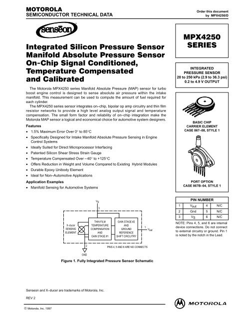
The Motorola MPX4250 series <strong>Manifold</strong> <strong>Absolute</strong> <strong>Pressure</strong> (MAP) sensor for turbo<br />
boost engine control is designed to sense absolute air pressure within the intake<br />
manifold. This measurement can be used to compute the amount of fuel required for<br />
each cylinder.<br />
The MPX4250 series sensor integrates on–chip, bipolar op amp circuitry and thin film<br />
resistor networks to provide a high level analog output signal and temperature<br />
compensation. The small form factor and reliability of on–chip integration make the<br />
Motorola MAP sensor a logical and economical choice for automotive system designers.<br />
Features<br />
• 1.5% Maximum Error Over 0° to 85°C<br />
• Specifically Designed for Intake <strong>Manifold</strong> <strong>Absolute</strong> <strong>Pressure</strong> Sensing in Engine<br />
Control Systems<br />
• Ideally Suited for Direct Microprocessor Interfacing<br />
• Patented <strong>Silicon</strong> Shear Stress Strain Gauge<br />
• Temperature Compensated Over –40° to +125°C<br />
• Offers Reduction in Weight and Volume Compared to Existing Hybrid Modules<br />
• Durable Epoxy Unibody Element<br />
• Ideal for Non–Automotive Applications<br />
Application Examples<br />
• <strong>Manifold</strong> Sensing for Automotive Systems<br />
X–ducer<br />
SENSING<br />
ELEMENT<br />
Motorola <strong>Sensor</strong> Device Data<br />
© Motorola, Inc. 1997<br />
2<br />
GND<br />
V S<br />
3<br />
THIN FILM<br />
TEMPERATURE<br />
COMPENSATION<br />
AND<br />
GAIN STAGE #1<br />
GAIN STAGE #2<br />
AND<br />
GROUND<br />
REFERENCE<br />
SHIFT CIRCUITRY<br />
PINS 4, 5 AND 6 ARE NO CONNECTS<br />
1 Vout<br />
Figure 1. Fully <strong>Integrated</strong> <strong>Pressure</strong> <strong>Sensor</strong> Schematic<br />
Senseon and X–ducer are trademarks of Motorola, Inc.<br />
REV 2<br />
Order this document<br />
by MPX4250/D<br />
<br />
<br />
INTEGRATED<br />
PRESSURE SENSOR<br />
20 to 250 kPa (2.9 to 36.3 psi)<br />
0.2 to 4.9 V OUTPUT<br />
BASIC CHIP<br />
CARRIER ELEMENT<br />
CASE 867–08, STYLE 1<br />
PORT OPTION<br />
CASE 867B–04, STYLE 1<br />
PIN NUMBER<br />
1 Vout 4 N/C<br />
2 Gnd 5 N/C<br />
3 VS 6 N/C<br />
NOTE: Pins 4, 5, and 6 are internal<br />
device connections. Do not connect<br />
to external circuitry or ground. Pin 1<br />
is noted by the notch in the Lead.<br />
1
MAXIMUM RATINGS(1)<br />
Parametrics Symbol Value Unit<br />
Overpressure(2) (P1 > P2) Pmax 400 kPa<br />
Burst <strong>Pressure</strong>(2) (P1 > P2) Pburst 1000 kPa<br />
Storage Temperature Tstg –40 to +125 °C<br />
Operating Temperature TA –40 to +125 °C<br />
1. TC = 25°C unless otherwise noted.<br />
2. Exposure beyond the specified limits may cause permanent damage or degradation to the device.<br />
OPERATING CHARACTERISTICS (VS = 5.1 Vdc, TA = 25°C unless otherwise noted, P1 > P2)<br />
Characteristic Symbol Min Typ Max Unit<br />
<strong>Pressure</strong> Range(1) POP 20 — 250 kPa<br />
Supply Voltage(2) VS 4.85 5.1 5.35 Vdc<br />
Supply Current Io — 7.0 10 mAdc<br />
Minimum <strong>Pressure</strong> Offset(3) (0 to 85°C)<br />
@ VS = 5.1 Volts<br />
Full Scale Output(4) (0 to 85°C)<br />
@ VS = 5.1 Volts<br />
Full Scale Span(5) (0 to 85°C)<br />
@ VS = 5.1 Volts<br />
VFSS 4.622 4.692 4.762 Vdc<br />
VFSS 4.622 4.692 4.762 Vdc<br />
VFSS 4.622 4.692 4.762 Vdc<br />
Accuracy(6) (0 to 85°C) — — — ±1.5 %VFSS<br />
Sensitivity ΔV/ΔP — 20 — mV/kPa<br />
Response Time(7) tR — 1.0 — ms<br />
Output Source Current at Full Scale Output lo+ — 0.1 — mAdc<br />
Warm–Up Time(8) — — 20 — ms<br />
Offset Stability(9) — — ± 0.5 — %VFSS<br />
Decoupling circuit shown in Figure 3 required to meet electrical specifications.<br />
MECHANICAL CHARACTERISTICS<br />
Characteristics Symbol Min Typ Max Unit<br />
Weight, Basic Element (Case 867) — — 4.0 — Grams<br />
Common Mode Line <strong>Pressure</strong>(10) — — — 690 kPa<br />
NOTES:<br />
1. 1.0 kPa (kiloPascal) equals 0.145 psi.<br />
2. Device is ratiometric within this specified excitation range.<br />
3. Offset (Voff) is defined as the output voltage at the minimum rated pressure.<br />
4. Full Scale Output (VFSO) is defined as the output voltage at the maximum or full rated pressure.<br />
5. Full Scale Span (VFSS) is defined as the algebraic difference between the output voltage at full rated pressure and the output voltage at the<br />
minimum rated pressure.<br />
6. Accuracy (error budget) consists of the following:<br />
• Linearity: Output deviation from a straight line relationship with pressure over the specified pressure range.<br />
• Temperature Hysteresis: Output deviation at any temperature within the operating temperature range, after the temperature is<br />
cycled to and from the minimum or maximum operating temperature points, with zero differential pressure<br />
applied.<br />
• <strong>Pressure</strong> Hysteresis: Output deviation at any pressure within the specified range, when this pressure is cycled to and from the<br />
minimum or maximum rated pressure, at 25°C.<br />
• TcSpan: Output deviation over the temperature range of 0° to 85°C, relative to 25°C.<br />
• TcOffset: Output deviation with minimum rated pressure applied, over the temperature range of 0° to 85°C, relative<br />
to 25°C.<br />
• Variation from Nominal: The variation from nominal values, for Offset or Full Scale Span, as a percent of VFSS, at 25°C.<br />
7. Response Time is defined as the time for the incremental change in the output to go from 10% to 90% of its final value when subjected to<br />
a specified step change in pressure.<br />
8. Warm–up is defined as the time required for the product to meet the specified output voltage after the <strong>Pressure</strong> has been stabilized.<br />
9. Offset stability is the product’s output deviation when subjected to 1000 hours of Pulsed <strong>Pressure</strong>, Temperature Cycling with Bias Test.<br />
10. Common mode pressures beyond what is specified may result in leakage at the case–to–lead interface.<br />
2 Motorola <strong>Sensor</strong> Device Data
WIRE BOND<br />
LEAD FRAME<br />
SILICONE<br />
DIE COAT<br />
DIE<br />
ÉÉÉÉÉÉÉÉÉÉÉÉ<br />
ÉÉÉÉÉÉÉÉÉÉÉÉ<br />
ÉÉÉÉÉÉÉÉÉÉÉÉ<br />
ÉÉÉÉÉÉÉÉÉÉÉÉ<br />
SEALED VACUUM REFERENCE<br />
Figure 2. Cross–Sectional Diagram<br />
(Not to Scale)<br />
Motorola <strong>Sensor</strong> Device Data<br />
P1<br />
P2<br />
STAINLESS STEEL<br />
METAL COVER<br />
EPOXY<br />
CASE<br />
RTV DIE<br />
BOND<br />
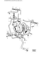
Figure 2 illustrates the absolute sensing chip in the basic<br />
chip carrier (Case 867). A fluorosilicone gel isolates the die<br />
surface and wire bonds from the environment, while allowing<br />
the pressure signal to be transmitted to the sensor diaphragm.<br />
The MPX4250A series pressure sensor operating<br />
characteristics, and internal reliability and qualification tests<br />
are based on use of dry air as the pressure media. Media,<br />
other than dry air, may have adverse effects on sensor performance<br />
and long–term reliability. Contact the factory for in-<br />
OUTPUT (Volts)<br />
5.0<br />
4.5<br />
4.0<br />
3.5<br />
3.0<br />
2.5<br />
2.0<br />
1.5<br />
1.0<br />
0.5<br />
0<br />
TRANSFER FUNCTION:<br />
Vout = VS* (0.004 x P–0.04) ± Error<br />
VS = 5.1 Vdc<br />
TEMP = 0 to 85°C<br />
0<br />
10<br />
20<br />
30<br />
40<br />
50<br />
60<br />
70<br />
80<br />
90<br />
100<br />
110<br />
MIN<br />
MPX4250A<br />
OUPUT<br />
(PIN 1)<br />
PRESSURE (ref: to sealed vacuum) in kPa<br />
50 pF<br />
51 k<br />
<br />
A/D<br />
μ PROCESSOR<br />
Figure 3. Typical Decoupling Filter for <strong>Sensor</strong> to<br />
Microprocessor Interface<br />
formation regarding media compatibility in your application.<br />
Figure 3 shows a typical decoupling circuit for interfacing<br />
the integrated MAP sensor to the A/D input of a microprocessor.<br />
Proper decoupling of the power supply is recommended.<br />
Figure 4 shows the sensor output signal relative to pressure<br />
input. Typical, minimum, and maximum output curves<br />
are shown for operation over temperature range of 0° to<br />
85°C. (The output will saturate outside of the specified pressure<br />
range.)<br />
MAX<br />
120<br />
130<br />
140<br />
150<br />
160<br />
170<br />
180<br />
190<br />
200<br />
210<br />
220<br />
230<br />
240<br />
250<br />
260<br />
Figure 4. Output versus <strong>Absolute</strong> <strong>Pressure</strong><br />
TYP<br />
3
Transfer Function<br />
Nominal Transfer Value: Vout = VS (P x 0.004 – 0.04)<br />
Nominal Transfer Value: +/– (<strong>Pressure</strong> Error x Temp. Factor x 0.004 x VS)<br />
Nominal Transfer Value: VS = 5.1 V ± 0.25 Vdc<br />
Temperature Error Band<br />
Temperature<br />
Error<br />
Factor<br />
4.0<br />
3.0<br />
2.0<br />
1.0<br />
0.0<br />
MPX4250A Series<br />
Temp Multiplier<br />
– 40 3<br />
0 to 85 1<br />
+125 3<br />
–40 –20 0 20 40 60 80 100 120 140<br />
Temperature in C°<br />
NOTE: The Temperature Multiplier is a linear response from 0° to –40°C and from 85° to 125°C.<br />
<strong>Pressure</strong> Error Band<br />
<strong>Pressure</strong> Error (kPa)<br />
9.0<br />
6.0<br />
3.0<br />
–3.0<br />
– 6.0<br />
– 9.0<br />
25 50 75 100 125 150 175 200 225 250<br />
<strong>Pressure</strong> Error (Max)<br />
20 to 250 kPa ± 3.45 (kPa)<br />
<strong>Pressure</strong> in kPa<br />
ORDERING INFORMATION<br />
The MPX4250A series Turbo MAP silicon pressure sensors are available in the basic element package or with pressure port<br />
fittings that provide mounting ease and barbed hose connections.<br />
Device Type Options Case No. MPX Series Order No. Marking<br />
Basic Element <strong>Absolute</strong>, Element Case 867–08 MPX4250A MPX4250A<br />
<strong>Absolute</strong>, Ported Case 867B–04 MPX4250AP MPX4250AP<br />
Ported Elements <strong>Absolute</strong>, Stove Pipe Port Case 867E–03 MPX4250AS MPX4250A<br />
<strong>Absolute</strong>, Axial Port Case 867F–03 MPX4250ASX MPX4250A<br />
4 Motorola <strong>Sensor</strong> Device Data
C<br />
J<br />
B<br />
–T–<br />
R<br />
J<br />
S<br />
Motorola <strong>Sensor</strong> Device Data<br />
C<br />
SEATING<br />
PLANE<br />
N<br />
M<br />
–A–<br />
PIN 1<br />
SEATING –T–<br />
PLANE<br />
B<br />
–P–<br />
0.25 (0.010) M T Q<br />
PIN 1<br />
M<br />
G<br />
F<br />
PACKAGE DIMENSIONS<br />
R<br />
1 2 3 4 5 6<br />
F<br />
V<br />
D 6 PL<br />
G<br />
N<br />
L<br />
0.136 (0.005) M T<br />
CASE 867–08<br />
ISSUE N<br />
POSITIVE PRESSURE<br />
(P1)<br />
BASIC ELEMENT (D)<br />
A<br />
U<br />
L<br />
1 2 3 4 5 6<br />
D 6 PL<br />
CASE 867B–04<br />
ISSUE E<br />
PRESSURE SIDE PORTED (AP)<br />
S<br />
A<br />
M<br />
PORT #1<br />
POSITIVE<br />
PRESSURE (P1)<br />
–Q–<br />
K<br />
0.13 (0.005) M T P S Q S<br />
STYLE 1:<br />
PIN 1. VOUT<br />
2. GROUND<br />
3. VCC<br />
4. V1<br />
5. V2<br />
6. VEX<br />
<br />
NOTES:<br />
1. DIMENSIONING AND TOLERANCING PER ANSI<br />
Y14.5M, 1982.<br />
2. CONTROLLING DIMENSION: INCH.<br />
3. DIMENSION –A– IS INCLUSIVE OF THE MOLD<br />
STOP RING. MOLD STOP RING NOT TO EXCEED<br />
16.00 (0.630).<br />
INCHES MILLIMETERS<br />
DIM MIN MAX MIN MAX<br />
A 0.595 0.630 15.11 16.00<br />
B 0.514 0.534 13.06 13.56<br />
C 0.200 0.220 5.08 5.59<br />
D 0.027 0.033 0.68 0.84<br />
F 0.048 0.064 1.22 1.63<br />
G 0.100 BSC 2.54 BSC<br />
J 0.014 0.016 0.36 0.40<br />
L 0.695 0.725 17.65 18.42<br />
M 30 NOM 30 NOM<br />
N 0.475 0.495 12.07 12.57<br />
R 0.430 0.450 10.92 11.43<br />
S 0.090 0.105 2.29 2.66<br />
NOTES:<br />
1. DIMENSIONING AND TOLERANCING PER ANSI<br />
Y14.5M, 1982.<br />
2. CONTROLLING DIMENSION: INCH.<br />
INCHES MILLIMETERS<br />
DIM MIN MAX MIN MAX<br />
A 1.145 1.175 29.08 29.85<br />
B 0.685 0.715 17.40 18.16<br />
C 0.305 0.325 7.75 8.26<br />
D 0.027 0.033 0.68 0.84<br />
F 0.048 0.064 1.22 1.63<br />
G 0.100 BSC 2.54 BSC<br />
J 0.014 0.016 0.36 0.41<br />
K 0.695 0.725 17.65 18.42<br />
L 0.290 0.300 7.37 7.62<br />
N 0.420 0.440 10.67 11.18<br />
P 0.153 0.159 3.89 4.04<br />
Q 0.153 0.159 3.89 4.04<br />
R 0.230 0.250 5.84 6.35<br />
S 0.220 0.240 5.59 6.10<br />
U 0.910 BSC 23.11 BSC<br />
V 0.182 0.194 4.62 4.93<br />
STYLE 1:<br />
PIN 1. V OUT<br />
2. GROUND<br />
3. V CC<br />
4. V1<br />
5. V2<br />
6. V EX<br />
5
V<br />
–B–<br />
PORT #1<br />
POSITIVE<br />
PRESSURE<br />
(P1)<br />
PORT #1<br />
POSITIVE<br />
PRESSURE<br />
(P1)<br />
V<br />
C<br />
J<br />
E<br />
C<br />
N E<br />
–T–<br />
–P–<br />
–T–<br />
J<br />
PACKAGE DIMENSIONS – continued<br />
K<br />
0.25 (0.010) M T<br />
S<br />
G<br />
0.13 (0.005) M T P S<br />
D 6 PL<br />
Q S<br />
A<br />
6 5 4 3 2 1<br />
F<br />
CASE 867E–03<br />
ISSUE D<br />
PRESSURE SIDE PORTED (AS)<br />
Q<br />
M<br />
F<br />
A<br />
U<br />
6 5 4 3 2 1<br />
CASE 867F–03<br />
ISSUE D<br />
PRESSURE SIDE PORTED (ASX)<br />
NOTES:<br />
1. DIMENSIONING AND TOLERANCING PER ANSI<br />
Y14.5M, 1982.<br />
2. CONTROLLING DIMENSION: INCH.<br />
STYLE 1:<br />
PIN 1. V OUT<br />
2. GROUND<br />
3. V CC<br />
4. V1<br />
5. V2<br />
6. V EX<br />
6 Motorola <strong>Sensor</strong> Device Data<br />
G<br />
D 6 PL<br />
PIN 1<br />
0.13 (0.005) M T<br />
K<br />
PIN 1<br />
N<br />
S<br />
R<br />
B<br />
B<br />
M<br />
–Q–<br />
INCHES MILLIMETERS<br />
DIM MIN MAX MIN MAX<br />
A 0.690 0.720 17.53 18.28<br />
B 0.245 0.255 6.22 6.48<br />
C 0.780 0.820 19.81 20.82<br />
D 0.027 0.033 0.69 0.84<br />
E 0.178 0.186 4.52 4.72<br />
F 0.048 0.064 1.22 1.63<br />
G 0.100 BSC 2.54 BSC<br />
J 0.014 0.016 0.36 0.41<br />
K 0.345 0.375 8.76 9.53<br />
N 0.300 0.310 7.62 7.87<br />
S 0.220 0.240 5.59 6.10<br />
V 0.182 0.194 4.62 4.93<br />
NOTES:<br />
1. DIMENSIONING AND TOLERANCING PER<br />
ANSI Y14.5M, 1982.<br />
2. CONTROLLING DIMENSION: INCH.<br />
INCHES MILLIMETERS<br />
DIM MIN MAX MIN MAX<br />
A 1.080 1.120 27.43 28.45<br />
B 0.740 0.760 18.80 19.30<br />
C 0.630 0.650 16.00 16.51<br />
D 0.027 0.033 0.68 0.84<br />
E 0.160 0.180 4.06 4.57<br />
F 0.048 0.064 1.22 1.63<br />
G 0.100 BSC 2.54 BSC<br />
J 0.014 0.016 0.36 0.41<br />
K 0.220 0.240 5.59 6.10<br />
N 0.070 0.080 1.78 2.03<br />
P 0.150 0.160 3.81 4.06<br />
Q 0.150 0.160 3.81 4.06<br />
R 0.440 0.460 11.18 11.68<br />
S 0.695 0.725 17.65 18.42<br />
U 0.840 0.860 21.34 21.84<br />
V 0.182 0.194 4.62 4.93<br />
STYLE 1:<br />
PIN 1. V OUT<br />
2. GROUND<br />
3. V CC<br />
4. V1<br />
5. V2<br />
6. V EX