How the I2C Bus Works - EEWeb
How the I2C Bus Works - EEWeb
How the I2C Bus Works - EEWeb

Create successful ePaper yourself
Turn your PDF publications into a flip-book with our unique Google optimized e-Paper software.
<strong>How</strong> <strong>the</strong> I 2 C <strong>Bus</strong> <strong>Works</strong><br />
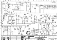
The I 2 C (Inter-Integrated Circuit) <strong>Bus</strong> is a two-wire, low to medium speed, communication<br />
bus (a path for electronic signals) developed by Philips Semiconductors in <strong>the</strong> early<br />
1980s. I 2 C was created to reduce <strong>the</strong> manufacturing costs of electronic products.<br />
Low Cost<br />
Prior to I 2 C, chip-to-chip communications used<br />
many pins in a parallel interface. Many of <strong>the</strong>se<br />
pins were used for inter-chip addressing,<br />
selection, control, and data transfers. In a parallel<br />
interface, 8 data bits are typically transferred from<br />
a sender IC to a receiver IC in a single operation.<br />
I 2 C performs chip-to-chip communications using<br />
only two wires in a serial interface, allowing ICs to<br />
communicate with fewer pins. The two wires in<br />
<strong>the</strong> I 2 C <strong>Bus</strong> carry addressing, selection, control,<br />
and data, one bit at a time. The Data (SDA) wire<br />
carries <strong>the</strong> data, while <strong>the</strong> Clock (SCL) wire<br />
synchronizes <strong>the</strong> sender and receiver during <strong>the</strong><br />
transfer. ICs that use <strong>the</strong> I 2 C <strong>Bus</strong> can perform <strong>the</strong><br />
same function as <strong>the</strong>ir larger parallel interface<br />
counterparts, but with far fewer pins.<br />
Semiconductors 3<br />
Courtesy of www.mcc-us.com