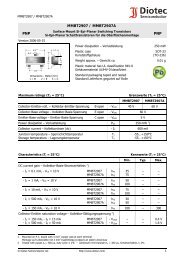
HDSP-Ax11
HDSP-Ax11
HDSP-Ax11

Create successful ePaper yourself
Turn your PDF publications into a flip-book with our unique Google optimized e-Paper software.
<strong>HDSP</strong>-<strong>Ax11</strong><br />
Black Surface Seven Segment Displays<br />
Data Sheet<br />
<strong>HDSP</strong>-AX11/-AX13 Series, <strong>HDSP</strong>-FX11/-FX13 Series<br />
<strong>HDSP</strong>-GX11/-GX13 Series, <strong>HDSP</strong>-HX11/-HX13 Series<br />
<strong>HDSP</strong>-KX11/-KX13 Series<br />
Description<br />
These devices use industry standard size package<br />
and pinout. Available with black surface finish. All<br />
devices are available as either common anode or<br />
common cathode.<br />
Typical applications include appliances, channel<br />
indicators of TV, CATV converters, game machines,<br />
and point of sale terminals.<br />
Devices<br />
Features<br />
• Black surface and color tinted epoxy<br />
• Industry standard size<br />
• Industry standard pinout<br />
• Choice of character size<br />
7.6 mm (0.30 in.), 10 mm (0.40 in.), 14.2 mm (0.56 in.)<br />
• Choice of colors<br />
AlGaAs Red, High Efficiency Red (HER), Green, Orange<br />
• Excellent appearance<br />
Evenly lighted segments<br />
± 50° Viewing angle<br />
• Design flexibility<br />
Common anode or common cathode<br />
Single and two digit<br />
• Categorized for luminous intensity<br />
Categorized for color: Green<br />
Use of like categories yields a uniform display<br />
• Excellent for long digit string multiplexing<br />
Orange<br />
AlGaAs<br />
Red HER Green Package<br />
<strong>HDSP</strong>- <strong>HDSP</strong>- <strong>HDSP</strong>- <strong>HDSP</strong>- Description Drawing<br />
A411 A111 A211 A511 7.6 mm Common Anode Right Hand Decimal A<br />
A413 A113 A213 A513 7.6 mm Common Cathode Right Hand Decimal B<br />
F411 F111 F211 F511 10 mm Common Anode Right Hand Decimal C<br />
F413 F113 F213 F513 10 mm Common Cathode Right Hand Decimal D<br />
G411 G111 G211 G511 10 mm Two Digit Common Anode Right Hand Decimal E<br />
G413 G113 G213 G513 10 mm Two Digit Common Cathode Right Hand Decimal F<br />
H411 H111 H211 H511 14.2 mm Common Anode Right Hand Decimal G<br />
H413 H113 H213 H513 14.2 mm Common Cathode Right Hand Decimal H<br />
K411 K111 K211 K511 14.2 mm Two Digit Common Anode Right Hand Decimal I<br />
K413 K113 K213 K513 14.2 mm Two Digit Common Cathode Right Hand Decimal J
Part Numbering System<br />
5082 - X X X X-X X X X X<br />
<strong>HDSP</strong>-X X X X-X X X X X<br />
Notes:<br />
1. For codes not listed in the figure above, please refer to the respective datasheet or contact your nearest Avago<br />
representative for details.<br />
2. Bin options refer to shippable bins for a part number. Color and Intensity Bins are typically restricted to 1 bin per tube<br />
(exceptions may apply). Please refer to respective datasheet for specific bin limit information.<br />
2<br />
Mechanical Options [1]<br />
00: No Mechanical Option<br />
Color Bin Options [1,2]<br />
0: No Color Bin Limitation<br />
Maximum Intensity Bin [1,2]<br />
0: No Maximum Intensity Bin Limitation<br />
Minimum Intensity Bin [1,2]<br />
0: No Minimum Intensity Bin Limitation<br />
Device Configuration/Color [1]<br />
1: Common Anode<br />
3: Common Cathode<br />
Device Specific Configuration [1]<br />
Refer to Respective Datasheet<br />
Package [1]<br />
A: 7.6 mm (0.3 inch) Single Digit Seven Segment Display<br />
F: 10 mm (0.4 inch) Single Digit Seven Segment Display<br />
G: 10 mm (0.4 inch) Dual Digit Seven Segment Display<br />
H: 14.2 mm (0.56 inch) Single Digit Seven Segment Display<br />
K: 14.2 mm (0.56 inch) Dual Digit Seven Segment Display
Package Dimensions (7.6 mm Series) Internal Circuit Diagram<br />
Package Dimensions (10 mm Series: Single) Internal Circuit Diagram<br />
3
Package Dimensions (10 mm Series: Two Digit) Internal Circuit Diagram<br />
4
Package Dimensions (14.2 mm Series: Single) Internal Circuit Diagram<br />
Package Dimensions (14.2 mm Series: Two Digit) Internal Circuit Diagram<br />
5<br />
2<br />
1<br />
DIGIT NO. 1 CATHODE
Absolute Maximum Ratings<br />
AlGaAs Red HER/Orange Green<br />
<strong>HDSP</strong>-X11X <strong>HDSP</strong>-X21X/X41X <strong>HDSP</strong>-X51X<br />
Description Series Series Series Units<br />
Average Power per Segment or DP 37 105 105 mW<br />
Peak Forward Current per Segment or DP 45 90 [1] 90 [3] mA<br />
DC Forward Current per Segment or DP 15 [5] 30 [2] 30 [4] mA<br />
Operating Temperature Range –20 to +100 –40 to +100 °C<br />
Storage Temperature Range –55 to +100 °C<br />
Reverse Voltage per Segment or DP 3.0 V<br />
Wave Soldering Temperature for 3 Seconds 250 °C<br />
(1.60 mm [0.063 in.] below Body)<br />
Notes:<br />
1. See Figure 5 to establish pulsed conditions.<br />
2. Derate above 53°C at 0.45 mA/°C (see Figure 7).<br />
3. See Figure 6 to establish pulsed conditions.<br />
4. Derate above 39°C at 0.37 mA/°C (see Figure 7).<br />
5. Derate above 91°C at 0.53 mA/°C (see Figure 1).<br />
Electrical/Optical Characteristics at TA = 25°C<br />
AlGaAs Red<br />
Device Series<br />
<strong>HDSP</strong>- Parameter Symbol Min. Typ. Max. Units Test Conditions<br />
A11X Luminous Intensity/Segment [1,2] IV 315 600 µcd IF = 1 mA<br />
(Digit Average)<br />
3600 IF = 5 mA<br />
F11X, G11X 330 650 IF = 1 mA<br />
3900 IF = 5 mA<br />
H11X, K11X 400 700 IF = 1 mA<br />
4200 IF = 5 mA<br />
All Devices Forward Voltage/Segment or DP VF 1.6 2.0 V IF = 1 mA<br />
1.7 IF = 5 mA<br />
1.8 22 IF = 20 mA Peak<br />
Peak Wavelength lPEAK 645 nm<br />
6<br />
Dominant Wavelength [3] ld 637 nm<br />
Reverse Voltage/Segment or DP [4] VR 3.0 15 V IR = 100 µA<br />
Temperature Coefficient of<br />
VF/Segment or DP<br />
∆VF/°C -2 mV/°C<br />
A11X Thermal Resistance LED RqJ-PIN 255 °C/W/<br />
F11X, G11X<br />
Junction-to-Pin<br />
320<br />
Seg.<br />
H11X, K12X 400
Orange<br />
Device Series<br />
<strong>HDSP</strong>- Parameter Symbol Min. Typ. Max. Units Test Conditions<br />
A41X Luminous Intensity/Segment IV 0.70 mcd IF = 5 mA<br />
F41X, G41X (Segment Average) [1,2]<br />
1.0 IF = 5 mA<br />
H41X, K41X 2.37 IF = 10 mA<br />
All Forward Voltage/Segment or DP VF 2.0 2.5 V IF = 20 mA<br />
Devices<br />
Peak Wavelength lPEAK 600 nm<br />
High Efficiency Red<br />
Device Series<br />
<strong>HDSP</strong>- Parameter Symbol Min. Typ. Max. Units Test Conditions<br />
A21X Luminous Intensity/Segment [1,2] IV 360 980 µcd IF = 5 mA<br />
(Digit Average) 5390 IF = 20 mA<br />
F21X, G21X 420 1200 IF = 5 mA<br />
H21X, K21X 900 2800 IF = 10 mA<br />
3700 IF = 60 mA Peak:<br />
1/6 Duty Factor<br />
All Forward Voltage/Segment or DP VF 2.0 2.5 V IF = 20 mA<br />
Devices<br />
Peak Wavelength lPEAK 635 nm<br />
7<br />
Dominant Wavelength [3] ld 603 nm<br />
Reverse Voltage/Segment or DP [4] VR 3.0 30 V IR = 100 µA<br />
Temperature Coefficient of ∆VF/°C –2 mV/°C<br />
VF/Segment or DP<br />
A41X Thermal Resistance LED RqJ-PIN 200 °C/W/<br />
F41X, G41X<br />
Junction-to-Pin<br />
320<br />
Seg.<br />
H41X, K41X 345<br />
Dominant Wavelength [3] ld 626 nm<br />
Reverse Voltage/Segment or DP [4] VR 3.0 30 V IR = 100 µA<br />
Temperature Coefficient of ∆VF/°C -2 mV/°C<br />
VF/Segment or DP<br />
A21X Thermal Resistance LED RqJ-PIN 200 °C/W/<br />
F21X, G21X<br />
Junction-to-Pin<br />
320<br />
Seg.<br />
H21X, K21X 345
High Performance Green<br />
Device Series<br />
<strong>HDSP</strong>- Parameter Symbol Min. Typ. Max. Units Test Conditions<br />
A51X Luminous Intensity/Segment [1,2] IV 860 3000 µcd IF = 10 mA<br />
(Digit Average) 6800 IF = 20 mA<br />
F51X, G51X 1030 3500 IF = 10 mA<br />
H51X, K51X 900 2500 IF = 10 mA<br />
3100 IF = 60 mA Peak:<br />
1/6 Duty Factor<br />
All Forward Voltage/Segment or DP VF 2.1 2.5 V IF = 10 mA<br />
Devices Peak Wavelength lPEAK 566 nm<br />
Dominant Wavelength [3,5] ld 571 577 nm<br />
Reverse Voltage/Segment or DP [4] VR 3.0 50 V IR = 100 µA<br />
Temperature Coefficient of<br />
VF/Segment or DP<br />
∆VF/°C -2 mV/°C<br />
A51X Thermal Resistance LED RqJ-PIN 200 °C/W/<br />
F51X, G51X Junction-to-Pin 320<br />
Seg.<br />
H51X, K51X 345<br />
Notes:<br />
1. Case temperature of device immediately prior to the intensity measurement is 25°C.<br />
2. The digits are categorized for luminous intensity. The intensity category is designated by a letter on the side of the package.<br />
3. The dominant wavelength, ld, is derived from the CIE chromaticity diagram and is that single wavelength which defines the color of the device.<br />
4. Typical specification for reference only. Do not exceed absolute maximum ratings.<br />
5. Green (<strong>HDSP</strong>-A51X/F51X/G51X/H512X/K51X) series displays are categorized for dominant wavelength. The category is designated by a number<br />
adjacent to the luminous intensity category letter.<br />
8
AlGaAs Red<br />
I F AVE. MAX – MAXIMUM AVERAGE<br />
FORWARD CURRENT PER SEGMENT – mA<br />
Figure 1. Maximum allowable average or dc<br />
current vs. ambient temperature.<br />
RELATIVE LUMINOUS INTENSITY<br />
(NORMALIZED TO 1 AT 1 mA)<br />
Figure 3. Relative luminous intensity vs. dc<br />
forward current.<br />
9<br />
20<br />
18<br />
16<br />
14<br />
12<br />
10<br />
8<br />
6<br />
4<br />
R = 770°C/W<br />
θ J-A<br />
2<br />
0<br />
20 30 40 50 60 70 80 90 100 110 120<br />
20<br />
10<br />
5<br />
2<br />
1<br />
0.5<br />
0.2<br />
T – AMBIENT TEMPERATURE – °C<br />
A<br />
0.1<br />
0.1 0.2 0.5 1 2 5 10 20<br />
I F – FORWARD CURRENT<br />
PER SEGMENT – mA<br />
50.0<br />
20.0<br />
10.0<br />
5.0<br />
2.0<br />
1.0<br />
0.5<br />
0.1<br />
0 0.5 1.0 1.5 2.0 2.5<br />
V<br />
F<br />
– FORWARD VOLTAGE – V<br />
Figure 2. Forward current vs. forward voltage.<br />
I F – FORWARD CURRENT<br />
I PEAK – PEAK FORWARD CURRENT<br />
PER SEGMENT – mA<br />
PER SEGMENT – mA<br />
η PEAK–<br />
RELATIVE EFFICIENCY –<br />
NORMALIZED TO 1 AT 1 mA<br />
1.3<br />
1.2<br />
1.1<br />
1.0<br />
0.9<br />
0.8<br />
0.5 mA<br />
0.7<br />
0 5 10 20 30 40 50<br />
Figure 4. Relative efficiency (luminous intensity per unit<br />
current) vs. peak current.
HER, Green, Orange<br />
RATIO OF MAXIMUM OPERATING<br />
PEAK CURRENT TO TEMPERATURE<br />
DERATED DC CURRENT<br />
I F PEAK<br />
I DC MAX<br />
I DC MAX – MAXIMUM DC CURRENT<br />
PER SEGMENT – mA<br />
Figure 7. Maximum allowable dc current vs.<br />
ambient temperature.<br />
ηPEAK – RELATIVE LUMINOUS INTENSITY<br />
(NORMALIZED TO 1 AT 5 mA FOR HER,<br />
AND TO 1 AT 10 mA FOR GREEN)<br />
Figure 9. Relative luminous intensity vs. dc<br />
forward current.<br />
10<br />
50<br />
45<br />
40<br />
35<br />
30<br />
25<br />
20<br />
15<br />
10<br />
5<br />
100<br />
10<br />
1<br />
1<br />
GREEN<br />
R = 770°C/W<br />
θ J-A<br />
HER / ORANGE<br />
0<br />
20 30 40 50 60 70 80 90 100 110 120<br />
T A – AMBIENT TEMPERATURE – °C<br />
12<br />
10<br />
8<br />
6<br />
4<br />
2<br />
0<br />
0<br />
10 KHz<br />
3 KHz<br />
300 Hz<br />
1 Hz<br />
t – PULSE DURATION – µs<br />
P<br />
HER / ORANGE<br />
GREEN<br />
100 Hz<br />
10 100 1000 10000<br />
Figure 5. Maximum tolerable peak current vs. pulse<br />
duration – HER, Orange.<br />
5 10 15 20 25 30<br />
I – FORWARD CURRENT PER SEGMENT – mA<br />
F<br />
OPERATION IN THIS<br />
REGION REQUIRES<br />
TEMPERATURE<br />
DERATING OF IDC<br />
MAXIMUM<br />
DC OPERATION<br />
RATIO OF MAXIMUM OPERATING<br />
PEAK CURRENT TO TEMPERATURE<br />
DERATED DC CURRENT<br />
I F PEAK<br />
I DC MAX<br />
Figure 6. Maximum tolerable peak current vs.<br />
pulse duration – Green.<br />
I F – FORWARD CURRENT PER SEGMENT – mA<br />
100<br />
80<br />
60<br />
40<br />
20<br />
HER / ORANGE<br />
GREEN<br />
0<br />
0 1.0 2.0 3.0 4.0 5.0<br />
V – FORWARD VOLTAGE – V<br />
F<br />
Figure 8. Forward current vs. forward voltage<br />
characteristics.<br />
ηPEAK – RELATIVE EFFICIENCY<br />
(NORMALIZED TO 1 AT 5 mA FOR HER,<br />
AND 10 mA FOR GREEN)<br />
100<br />
10<br />
1<br />
1<br />
1.8<br />
1.6<br />
1.4<br />
1.2<br />
1.0<br />
0.8<br />
0<br />
10 KHz<br />
3 KHz<br />
10 100 1000 10000<br />
t – PULSE DURATION – µs<br />
P<br />
GREEN<br />
300 Hz<br />
HER / ORANGE<br />
20 40 60 80<br />
100 Hz<br />
I PEAK – PEAK FORWARD CURRENT<br />
PER SEGMENT – mA<br />
OPERATION IN THIS<br />
REGION REQUIRES<br />
TEMPERATURE<br />
DERATING OF I DC<br />
MAXIMUM<br />
Figure 10. Relative efficiency (luminous intensity per unit<br />
current) vs. peak current.<br />
1 KHz<br />
100<br />
DC OPERATION
Intensity Bin Limits (mcd)<br />
AlGaAs Red<br />
<strong>HDSP</strong>-A1xx<br />
IV Bin Category Min. Max.<br />
E 0.315 0.520<br />
F 0.428 0.759<br />
G 0.621 1.16<br />
H 0.945 1.71<br />
I 1.40 2.56<br />
J 2.10 3.84<br />
K 3.14 5.75<br />
L 4.70 8.55<br />
<strong>HDSP</strong>-F1xx/G1xx<br />
IV Bin Category Min. Max.<br />
D 0.391 0.650<br />
E 0.532 0.923<br />
F 0.755 1.39<br />
G 1.13 2.08<br />
H 1.70 3.14<br />
<strong>HDSP</strong>-H1xx/K1xx<br />
IV Bin Category Min. Max.<br />
C 0.415 0.690<br />
D 0.565 0.990<br />
E 0.810 1.50<br />
F 1.20 2.20<br />
G 1.80 3.30<br />
H 2.73 5.00<br />
I 4.09 7.50<br />
11<br />
Orange<br />
<strong>HDSP</strong>-A41X<br />
IV Bin Category Min Max<br />
A 0.284 0.433<br />
B 0.354 0.541<br />
C 0.443 0.677<br />
D 0.554 0.846<br />
E 0.692 1.057<br />
F 0.856 1.322<br />
G 1.082 1.652<br />
H 1.352 2.066<br />
I 1.692 2.581<br />
J 2.114 3.227<br />
K 2.641 4.034<br />
L 3.300 5.042<br />
M 4.127 6.303<br />
N 5.157 7.878<br />
<strong>HDSP</strong>-F41X/G41X<br />
IV Bin Category Min Max<br />
C 0.485 0.890<br />
D 0.728 1.333<br />
E 1.091 2.000<br />
F 1.636 3.000<br />
G 2.454 4.500<br />
H 3.682 6.751<br />
<strong>HDSP</strong>-H41X/K41X<br />
IV Bin Category Min Max<br />
B 0.77 1.17<br />
C 0.95 1.45<br />
D 1.19 1.82<br />
E 1.49 2.27<br />
F 1.85 2.89<br />
G 2.32 3.54<br />
H 2.90 4.43
Intensity Bin Limits (mcd), continued<br />
HER<br />
<strong>HDSP</strong>-A2xx<br />
IV Bin Category Min. Max.<br />
B 0.342 0.630<br />
C 0.516 0.946<br />
D 0.774 1.418<br />
E 1.160 2.127<br />
F 1.740 3.190<br />
G 2.610 4.785<br />
H 3.915 7.177<br />
<strong>HDSP</strong>-F2xx/G2xx<br />
IV Bin Category Min. Max.<br />
C 0.485 0.890<br />
D 0.728 1.333<br />
E 1.091 2.000<br />
F 1.636 3.000<br />
G 2.454 4.500<br />
H 3.682 6.751<br />
<strong>HDSP</strong>-H2xx/K2xx<br />
IV Bin Category Min. Max.<br />
E 0.91 1.67<br />
F 1.37 2.51<br />
G 2.05 3.76<br />
H 3.08 5.64<br />
I 4.62 8.64<br />
J 6.93 12.70<br />
K 10.39 19.04<br />
12
Intensity Bin Limits (mcd), continued<br />
Green<br />
<strong>HDSP</strong>-A5xx<br />
IV Bin Category Min. Max.<br />
H 0.86 1.58<br />
I 1.29 2.37<br />
J 1.94 3.55<br />
K 2.90 5.33<br />
L 4.37 8.01<br />
<strong>HDSP</strong>-F5xx/G5xx<br />
IV Bin Category Min. Max.<br />
H 1.54 2.82<br />
I 2.31 4.23<br />
J 3.46 6.34<br />
K 5.18 9.50<br />
L 7.78 14.26<br />
<strong>HDSP</strong>-H5xx/K5xx<br />
IV Bin Category Min. Max.<br />
E 0.91 1.67<br />
F 1.37 2.51<br />
G 2.05 3.76<br />
H 3.08 5.64<br />
I 4.61 8.46<br />
Color Categories<br />
Note:<br />
All categories are established for classification of products. Products may<br />
not be available in all categories. Please contact your Avago<br />
representatives for further clarification/information.<br />
13<br />
Dominant Wavelength (nm)<br />
Color Bin Min. Max.<br />
Green 2 573.00 577.00<br />
3 570.00 574.00<br />
4 567.00 571.00<br />
5 564.00 568.00<br />
Contrast Enhancement<br />
For information on contrast<br />
enhancement, please see<br />
Application Note 1015.<br />
Soldering/Cleaning<br />
For information on soldering<br />
LEDs, please refer to<br />
Application Note 1029.<br />
Electrical/Optical<br />
For more information on<br />
electrical/optical characteristics,<br />
please see Application Note<br />
1005.
For product information and a complete list of distributors, please go to our website: www.avagotech.com<br />
Avago, Avago Technologies, and the A logo are trademarks of Avago Technologies, Pte. in the United States and other countries.<br />
Data subject to change. Copyright © 2006 Avago Technologies Pte. All rights reserved. Obsoletes 5988-4433EN<br />
5989-2795EN April 10, 2006