VLSI at USC
VLSI at USC
VLSI at USC

Create successful ePaper yourself
Turn your PDF publications into a flip-book with our unique Google optimized e-Paper software.
<strong>VLSI</strong> <strong>at</strong> <strong>USC</strong><br />
Prepared by Melvin A. Breuer<br />
Charles Lee Powell Professor of Electrical Engineering and Computer Science<br />
June 2010<br />
Preface: Over the past 45 years I have advised many students regarding courses to<br />
take, helped others in getting their first engineering job, and discussed wh<strong>at</strong> areas are<br />
“hot.” As to the l<strong>at</strong>ter topic, I never give a student an opinion on wh<strong>at</strong> area seems to<br />
have the largest growth, or where jobs will be plentiful in 2-3 years. My advice in wh<strong>at</strong> a<br />
student should pursue is usually: (a) work in an area th<strong>at</strong> you think you will enjoy and<br />
where you think you have good insight and understanding, and (b) strive to be as good<br />
in this area as you can be with the talents and ability you have been given. But I also<br />
get somewh<strong>at</strong> easier questions to deal with like: “Wh<strong>at</strong> is <strong>VLSI</strong> about?” or “Wh<strong>at</strong> is<br />
EEXXX about?” or “Is EEYYY hard and does it have a project?” Well, to answer some<br />
of these questions I have prepared this document. It is not an official <strong>USC</strong> document; it<br />
is only my opinion and in some cases recommend<strong>at</strong>ions. But maybe it will help new<br />
M.S. and Ph.D. students get started in our EE <strong>VLSI</strong> program.<br />
1. Introduction<br />
There have been several technological revolutions over the last 2000 years, including<br />
the invention of printing press in the 15 th century, the Industrial Revolution of the 18 th<br />
century when the world turned from an agrarian society to one more oriented to<br />
manufacturing, mining and transport. Currently we are <strong>at</strong> the beginning of the<br />
inform<strong>at</strong>ion technology revolution th<strong>at</strong> started in about 1960, made commercially<br />
successful by the invention of transistors and integr<strong>at</strong>ed circuits, and now referred to as<br />
the age of very large scale integr<strong>at</strong>ion (<strong>VLSI</strong>).<br />
In 1959-60 I was an M.S. Student <strong>at</strong> UCLA. I went to Boston for an interview <strong>at</strong> M.I.T.<br />
The plane flew <strong>at</strong> about 600 mph. Last year I went to Washington D.C. Guess wh<strong>at</strong>!<br />
Again I flew <strong>at</strong> 600 mph. Has flying gotten better in these 50 years? Well maybe safer<br />
and more fuel efficient, but back then I had more leg room, better and free food, no<br />
charge for luggage, and was not tre<strong>at</strong>ed as c<strong>at</strong>tle. Where is the progress?<br />
Work on my on-campus job and M.S. Thesis required th<strong>at</strong> I do a lot of Fortran II<br />
programming. Since there were few computer users on campus in those days, I often<br />
had exclusive access to the IBM 650 from 2 to 4 AM. Of course, today I have<br />
instantaneous access to computing power and storage th<strong>at</strong> is <strong>at</strong> least 8 orders of<br />
magnitude large than I had back then. Unlike other revolutions th<strong>at</strong> depend on a<br />
quantum jump in technology, such as the invention of the telephone and discovery of<br />
AC electricity, the IT revolution is unique in th<strong>at</strong> every 15 months or so the hardware<br />
you recently purchases becomes obsolete in terms of the l<strong>at</strong>est performance. Clearly<br />
the airline industry is still waiting for a technological revolution.<br />
The Ming Hsieh Department of Electrical Engineering here <strong>at</strong> the Viterbi School of<br />
Engineering offers a stellar program in <strong>VLSI</strong> Systems and Circuits Engineering (<strong>VLSI</strong>-<br />
S&CE). Many of the faculty have received teaching and research awards, and have<br />
1<br />
Copyright 2010 M.A. Breuer
written textbooks used around the world. The tenure track faculty is complemented by a<br />
full-time teaching staff who have extensive industrial background and “teaching genes”,<br />
as well as researchers from our sister institution, the Inform<strong>at</strong>ion Science Institute (ISI)<br />
situ<strong>at</strong>ed in the Santa Monica Marina, and home to the <strong>VLSI</strong> MOSIS project.<br />
Below I summarize the components involved in the design and manufacturing of a<br />
<strong>VLSI</strong>-based system, and the core courses in our curricula th<strong>at</strong> train students to be<br />
successful engineers in these areas. I hope th<strong>at</strong> this memo will help you in making good<br />
decisions regarding your carrier and studies <strong>at</strong> <strong>USC</strong>.<br />
2. System flow<br />
Figures 1 and 2 indic<strong>at</strong>e simplified versions of the system flow involved in cre<strong>at</strong>ing a<br />
new digital <strong>VLSI</strong> ASIC chip. This is primarily a top-down process, while the design of<br />
fully custom chips pays more <strong>at</strong>tention to physical design consider<strong>at</strong>ion throughout the<br />
process and generally involves more designer-driven design r<strong>at</strong>her than RTL synthesis<br />
of critical components.<br />
Specific<strong>at</strong>ion: The process starts with a system specific<strong>at</strong>ion (spec) of the functionality<br />
of a chip. In addition, the spec usually includes inform<strong>at</strong>ion and/or constraint <strong>at</strong>tributes<br />
such as technology, packaging, power dissip<strong>at</strong>ion, die temper<strong>at</strong>ure, clock r<strong>at</strong>e,<br />
manufacturing cost, and performance. Often non-system designers develop part of<br />
these specs, usually in response to detailed discussions with potential customers. For<br />
example, the spec for the electronics in a new hearing aid might be developed in part by<br />
an expert in digital signal processing and an otologist. While our curricula does not<br />
directly address issues associ<strong>at</strong>ed with the development of specs, needless to say th<strong>at</strong><br />
background in other areas of EE, such as communic<strong>at</strong>ion theory and signal and image<br />
processing are very useful. One reason for this is th<strong>at</strong> while over 90% of chips<br />
manufactured each year may be characterized as being general purpose<br />
microprocessors, over 90% of chips designed each year are not microprocessors.<br />
Temporal and logical synthesis with constraints and goals<br />
System Synthesis: The first step in the design process is the human transform<strong>at</strong>ion of<br />
an implement<strong>at</strong>ion independent specific<strong>at</strong>ion and the functionality and performance<br />
specs into a flow of both parallel and sequential conditional comput<strong>at</strong>ional steps e.g.,<br />
d<strong>at</strong>a and control flow graphs. Key tasks during this process are (1) the selection of a<br />
suitable architecture, (2) decomposing the required functionality over the components of<br />
this architecture including decision about which functionality is implemented in hardware<br />
and which in software (to be run on a general purpose or embedded processor), and (3)<br />
scheduling the various activities so as to meet the performance specs. Part of this<br />
process deals with determining and analyzing various algorithms for instanti<strong>at</strong>ing the<br />
desired behaviors. For example there are many ways of building a Viterbi decoder. In<br />
addition to the algorithmic solution, one must also consider the non-behavioral aspects<br />
of the spec, such as imposed constraints and performance objectives. Since the actual<br />
design space is quite vast, autom<strong>at</strong>ion is often used to prune the space and to predict<br />
2<br />
Copyright 2010 M.A. Breuer
values of <strong>at</strong>tributes such as g<strong>at</strong>e count and power dissip<strong>at</strong>ion. Often languages such as<br />
hardware C or System C are used. The next step in the design process, namely<br />
behavioral synthesis, is highly intertwined with system synthesis.<br />
Behavioral Level Synthesis: The next step is to take the system description as a<br />
collection of interacting machine descriptions or d<strong>at</strong>a and control flow graphs and<br />
produce the system architecture in terms of wh<strong>at</strong> components are used to perform<br />
required oper<strong>at</strong>ions, how much sharing is desirable or possible, how are the various<br />
oper<strong>at</strong>ions scheduled, where the intermedi<strong>at</strong>e results of comput<strong>at</strong>ion are stored, how<br />
these components communic<strong>at</strong>e with each other, etc.<br />
The three main problems typically addressed in behavioral synthesis systems are<br />
alloc<strong>at</strong>ion of resources, scheduling of processes, and binding of variables to hardware<br />
entities.<br />
The binding of variables to hardware entities includes defining the bit-width of various<br />
elements. Some bit-widths may be determined <strong>at</strong> the higher behavioral level, but<br />
sometimes domain-expert algorithm designers work <strong>at</strong> the behavioral level and leave<br />
bit-width analysis to the hardware designers.<br />
Often languages such as Verilog, VHDL and System C are used to describe the<br />
behavior of a chip.<br />
Register Transfer Level Synthesis: System and behavioral synthesis are somewh<strong>at</strong><br />
like programming in a high level language and applying compiler-like transform<strong>at</strong>ions to<br />
optimize the program (in terms of its size or its execution time); you have all the<br />
variables, memory and oper<strong>at</strong>ors you want. But a chip consists of a finite number of<br />
g<strong>at</strong>es, flip-flops and memory, though this finite number is getting to be in the billions.<br />
Thus a behavioral description must be transformed into one th<strong>at</strong> rel<strong>at</strong>es variables,<br />
constants and oper<strong>at</strong>ors with hardware entities such as registers, memories, busses<br />
and blocks of logic. This transform<strong>at</strong>ion process, which over the past 15 years has been<br />
partially autom<strong>at</strong>ed, is referred to as register-transfer-level (RTL) synthesis. At this point<br />
various computer-aided design (CAD) tools can be employed th<strong>at</strong> predict <strong>at</strong>tributes of<br />
the final circuit if the design process were to be continued. Some of these <strong>at</strong>tributes<br />
include power dissip<strong>at</strong>ion, g<strong>at</strong>e count, area, yield and performance. So, <strong>at</strong> this point, a<br />
designer can make an intelligent decision as to whether to continue refining this design,<br />
or consider altern<strong>at</strong>ive behavioral and/or register solutions.<br />
The inputs to this step are a set of oper<strong>at</strong>ions described as transfer of values between<br />
registers and functional units through a hierarchy of interconnect structures including<br />
buses and multiplexers under the command of a hardware controller. The outputs of this<br />
step are blocks of combin<strong>at</strong>ional logic separ<strong>at</strong>ed by sequential circuit elements (l<strong>at</strong>ches<br />
and flip-flops). An important task performed in this step is the encoding and realiz<strong>at</strong>ion<br />
of the controller block (specified as a finite st<strong>at</strong>e machine or a collection of interacting<br />
machines) in hardware. Here is where your knowledge of FSM’s is essential.<br />
3<br />
Copyright 2010 M.A. Breuer
Logic synthesis: Logic synthesis is the process of taking wh<strong>at</strong> we normally think of as<br />
a logic design consisting of g<strong>at</strong>es, flip-flops, and clusters of flip-flops referred to as<br />
registers, and manipul<strong>at</strong>ing this digital circuit so th<strong>at</strong> it retains its functionality, but now<br />
s<strong>at</strong>isfies various constraints and optimizes various objectives. First, you need to<br />
recognize th<strong>at</strong> 2-level AND-OR on NAND-NAND logic is not encountered very often in<br />
real circuits. Most logic structures are multi-level, and include both primitive and<br />
complex g<strong>at</strong>es. Area, testability and performance (delay) are of prime concern. Thus,<br />
logic synthesis, which also is a highly autom<strong>at</strong>ed process, consists of oper<strong>at</strong>ions such<br />
as re-timing, library mapping/binding, fan-out optimiz<strong>at</strong>ion and g<strong>at</strong>e sizing.<br />
If the area, performance, or power does not meet your specific<strong>at</strong>ions, then re-design <strong>at</strong><br />
the RTL or behavioral level is needed.<br />
Well, <strong>at</strong> this point we finally have a design in terms of things we understand, namely<br />
g<strong>at</strong>es and flip-flops. Now lets go get out our soldering iron and build it in hardware.<br />
Physical synthesis<br />
Physical design is the process of mapping the output from temporal and logic synthesis<br />
into a form th<strong>at</strong> can be sent to a factory for manufacturing. The end product of physical<br />
synthesis is actually a set of masks in the form of a GDSII file. A mask is somewh<strong>at</strong><br />
analogous to a film neg<strong>at</strong>ive th<strong>at</strong> has millions of black rectangles exposed on a<br />
transparent sheet. One main difference is th<strong>at</strong> a set of masks costs several millions of<br />
dollars, so you do not get many chances to “capture th<strong>at</strong> moment.” Physical synthesis<br />
consists of several processes th<strong>at</strong> are mostly autom<strong>at</strong>ed, usually highly inter-rel<strong>at</strong>ed,<br />
but for simplicity, described here as separ<strong>at</strong>e entities.<br />
Partitioning: Normally a design is cre<strong>at</strong>ed where some objectives are the focus of<br />
<strong>at</strong>tention, but when the design is mapped into silicon, other factors become more<br />
important, such as chip area, power dissip<strong>at</strong>ion, signal delay and testability. One of the<br />
first steps in physical design is to partition the circuit into manageable units. The<br />
simplest example is to partition a design into several chips if it cannot “fit” onto one chip.<br />
On-chip partitions might aggreg<strong>at</strong>e circuitry th<strong>at</strong> runs off of a common clock, circuitry<br />
th<strong>at</strong> requires a voltage different from the rest of the logic, or circuitry th<strong>at</strong> is more<br />
susceptible to noise.<br />
Floorplanning: The layout of a chip is similar to the floorplan of a large home: there are<br />
usually several bedrooms, a living room, a dining room off of the kitchen, and a master<br />
b<strong>at</strong>hroom, another for children and one for guests. These must be str<strong>at</strong>egically placed<br />
according to total areas, the area and aspect r<strong>at</strong>io of the property, convenience, etc.<br />
The same is true for a chip, where, for example, a 64-bit ALU can be layed-out many<br />
different ways. Chip floorplans consists of alloc<strong>at</strong>ing specific resources and budgets to<br />
the various large modules in a design, such as control, I/O, image processing, ALU,<br />
wireless trans-receiver, and memory. These alloc<strong>at</strong>ed entities consists of items such as<br />
4<br />
Copyright 2010 M.A. Breuer
area, aspect r<strong>at</strong>io, loc<strong>at</strong>ion of I/O terminals, power, and available metal layers for<br />
interconnect.<br />
Placement: Eventually elements such as transistors, g<strong>at</strong>es and flip-flops must be<br />
assigned to physical coordin<strong>at</strong>es on the surface of a die so th<strong>at</strong> they are electrically<br />
isol<strong>at</strong>ed from one another, yet they can be electrically interconnected so th<strong>at</strong> they<br />
implement the desired specific<strong>at</strong>ion and the die area is near minimal. A simplified<br />
version of the placement problem is: given 1 million rectangles of various aspect r<strong>at</strong>ios,<br />
place them inside of a square boundary so th<strong>at</strong> no rectangle overlaps another one, and<br />
the area of the square is minimal.<br />
Interconnect (routing): Wh<strong>at</strong> makes the placement example given above a simplified<br />
case of the <strong>VLSI</strong> placement problem is th<strong>at</strong> an additional objective to be achieved is a<br />
placement so th<strong>at</strong> all terminals of each and every signal net can be made electrically<br />
common. This wiring of nets must be achieved while (1) not shorting any signal to<br />
another one, (2) minimizing the maximum signal propag<strong>at</strong>ion delay, (3) avoiding<br />
crosstalk, and much more. In some cases, there will be areas of the physical design th<strong>at</strong><br />
are limited by interconnect and wire-planning must be done in conjunction with<br />
floorplanning and placement.<br />
Miscellaneous Processes<br />
Library development: Normally placement and interconnect processes deal with a<br />
“g<strong>at</strong>e” level model of circuit elements. In reality, signals are processed via transistor<br />
circuits, and transistors and interconnect are defined by a set of rectangular images<br />
associ<strong>at</strong>ed with various layers of integr<strong>at</strong>ion, such as metal 1, 2, 3, …, polysilicon and<br />
oxide. Library development consists of developing a family of circuits, e.g., th<strong>at</strong> all<br />
implement a 3-input NAND function, but have different delay and drive capability. While<br />
much of this process is done manually, many tools exist to analyze these designs in<br />
terms of electrical and logical characteristics. One popular tool is SPICE (circuit-level)<br />
simul<strong>at</strong>ion. The results of this analysis is th<strong>at</strong> the each g<strong>at</strong>e in the library has a variety of<br />
abstract “views” to support timing analysis, digital simul<strong>at</strong>ion, physical design and<br />
verific<strong>at</strong>ion.<br />
Mask gener<strong>at</strong>ion: Once all elements have been placed and interconnected, the<br />
elements are replaced by their library images and the entire design is converted into a<br />
GDSII file. Due to the fact th<strong>at</strong> fe<strong>at</strong>ure sizes of transistors and wires are in the range of<br />
45 nm, and the wavelengths of light produced by lasers used in transferring these<br />
images onto silicon are comparable in scale, manufactured fe<strong>at</strong>ures differ from mask<br />
fe<strong>at</strong>ures. Thus a new field has emerged dealing with such concepts as doublep<strong>at</strong>terning<br />
and optical proximity correction (OPC).<br />
Testing: Gordon Moore noted th<strong>at</strong> a major shift in scaling of <strong>VLSI</strong> fe<strong>at</strong>ure sizes occurs<br />
about every 18 months. Over the last few years we have gone from 65nm in 2007, to 45<br />
nm in 2010 and soon to 32 nm in 2013. Why didn’t we just skip the 45nm technology<br />
node and come out with 32 nm instead? Well the answer is th<strong>at</strong> it is very difficult and<br />
5<br />
Copyright 2010 M.A. Breuer
costly to move from one node to another in terms of research, development and<br />
manufacturing equipment. Simply put, it is very costly. Thus, while researchers are<br />
currently working on 22nm and 14 nm nodes, the yields are still very low. Th<strong>at</strong> is, if one<br />
manufactured one million transistors, few if any would work as desired. It usually takes<br />
several years of tuning a technology to learn how to increase the yield to very high<br />
levels; this is the process known as “yield learning”. I leave it to the reader to calcul<strong>at</strong>e<br />
the minimum required probability of manufacturing a good transistor so th<strong>at</strong> if a chip has<br />
one-billion transistors, the probability of all of them are good is 0.5. Well the answer<br />
looks something like 0.999…9. As a result, it is estim<strong>at</strong>ed th<strong>at</strong> from 30-70% of complex<br />
(multi-million transistors) chips manufactured today using the l<strong>at</strong>est technology nodes<br />
are defective. Yet they all look the same. Manufacturing test is the process of<br />
separ<strong>at</strong>ing out the good chips from the bad ones. Again, most aspects of test<br />
development and testing itself have been autom<strong>at</strong>ed.<br />
Verific<strong>at</strong>ion: Going back once again to my days <strong>at</strong> UCLA, as it turned out, near the end<br />
of my tenure many people had learned how to program so the University got new<br />
machines and reverted to a close shop mode of oper<strong>at</strong>ion. In this situ<strong>at</strong>ion, I was forced<br />
to write my program in my lab, use a key punch machine to transcribe my program onto<br />
punch cards, walk my deck of cards across campus and leave it <strong>at</strong> the IN window. The<br />
next day I would return and if lucky my deck was there with a print out telling me all of<br />
my syntax errors. I would correct these and resubmit. Returning the next day, there<br />
might be nothing for me. Returning the following day I might have the results of a run,<br />
but because of a programming error I had to again resubmit my program. Thus weeks<br />
could go by before I would get a successful run. This process taught me the importance<br />
of writing a program correctly the first time. And yes, one day I had to write a program in<br />
SIR, an assembly language th<strong>at</strong> supported flo<strong>at</strong>ing-point oper<strong>at</strong>ions, and guess wh<strong>at</strong>, it<br />
worked properly the first time.<br />
Unfortun<strong>at</strong>ely, life is too easy now, and designers get instantaneous responses to their<br />
programs. Thus designers tend to work in the mode of trial and error. Hence each of the<br />
items mentioned above are subject to human errors and must be checked. Thus<br />
verific<strong>at</strong>ion is a primary tool associ<strong>at</strong>ed with design. Verific<strong>at</strong>ion must address many<br />
aspects of a design, such as its temporal <strong>at</strong>tributes, its electrical characteristics,<br />
n<strong>at</strong>urally the logic itself, and finally the physical characteristics. Properties must be<br />
checked th<strong>at</strong> were not intended to be part of the design, such as simultaneous switching<br />
noise, and ringing due to inductance. Verific<strong>at</strong>ion is one of the last frontiers in CAD th<strong>at</strong><br />
has not been successfully autom<strong>at</strong>ed.<br />
6<br />
Copyright 2010 M.A. Breuer
SoC Architecture<br />
Project evalu<strong>at</strong>ion/Feasibility study<br />
SoC specific<strong>at</strong>ion definition & docs<br />
SoC verific<strong>at</strong>ion plan definition & docs<br />
SoC implement<strong>at</strong>ion guidelines: clock reset, power,<br />
test modes, etc.<br />
SoC implement<strong>at</strong>ion guidelines: technology node, IO<br />
rings, performance constrains, oper<strong>at</strong>ing environment<br />
RTL Design<br />
Customer IP RTL code entry<br />
SoC RTL code entry<br />
IP integr<strong>at</strong>ion<br />
RTL simul<strong>at</strong>ion<br />
RLL Verific<strong>at</strong>ion<br />
RTL test bench verific<strong>at</strong>ion<br />
RTL valid<strong>at</strong>ion and assertions<br />
Logic coverage report<br />
RTL to Netlist<br />
RTL synthesis<br />
Timing constraints scrubbing-ideal clock<br />
Low power synthesis<br />
DFT insertion-JTAG, MBIST, Scan<br />
Formal verific<strong>at</strong>ion<br />
Figure 1: Avnet ASIC Israel SoC CAD Flow<br />
7<br />
Copyright 2010 M.A. Breuer<br />
AAI - Avnet ASIC<br />
Israel<br />
SoC CAD Flow<br />
Physical Implement<strong>at</strong>ion<br />
Floor plan<br />
Physical synthesis<br />
Clock tree & high fan-out<br />
Place & route<br />
Chip finishing: DFM utilities, seal ring,<br />
artifacts, etc.<br />
Design Verific<strong>at</strong>ion<br />
Extraction: 2.5D, DFM aware<br />
St<strong>at</strong>ic timing, DFM aware<br />
SI & reliability analysis: Xtalk, Irdro, EM<br />
G<strong>at</strong>e level simul<strong>at</strong>ion with back annot<strong>at</strong>ion<br />
Power measurements: st<strong>at</strong>ic/dynamic<br />
Physical Verific<strong>at</strong>ion<br />
LVS (layout vs. schem<strong>at</strong>ic check)<br />
DRC (design rule check)<br />
ERC (antenna, bonding etc.)<br />
Tape-Out<br />
Foundry checklists and forms<br />
GDSII transfer to Foundry<br />
Mask gener<strong>at</strong>ion review
Magna <strong>VLSI</strong> IC Design Flow<br />
Design specific<strong>at</strong>ion<br />
Behavioral description<br />
RTL description (HDL)<br />
Functional verific<strong>at</strong>ion and testing<br />
Logic synthesis<br />
G<strong>at</strong>e-level netlist<br />
Logic verific<strong>at</strong>ion and testing<br />
Floor planning, place and route<br />
Physical layout<br />
Layout verific<strong>at</strong>ion and implement<strong>at</strong>ion<br />
FAB<br />
Legend: Autom<strong>at</strong>ic Manual or semi-autom<strong>at</strong>ic<br />
Figure 2: Magna <strong>VLSI</strong> IC Design Flow<br />
8<br />
Copyright 2010 M.A. Breuer
3. Found<strong>at</strong>ion for silicon system construction<br />
Figure 3 indic<strong>at</strong>es the main constituents needed to build <strong>VLSI</strong> systems. At the heart of<br />
the system is the manufacturing/fabric<strong>at</strong>ion technology itself. CMOS circuitry has<br />
been the driving force in this field over the past 40 years, and will continue to be for <strong>at</strong><br />
least the next 15 years. Of course, radically different technologies are being developed,<br />
such as spintronics, nano-, bio-, chemical- and quantum-g<strong>at</strong>es. The cost of constructing<br />
a new wafer fabric<strong>at</strong>ion facility is over $1 billion. Our courses EE 504L deal with aspects<br />
of the fabric<strong>at</strong>ion process.<br />
Another pillar needed to support the development of <strong>VLSI</strong> systems is verific<strong>at</strong>ion.<br />
There are several reasons why this is such an important component. First is th<strong>at</strong> <strong>VLSI</strong><br />
systems are very complex. They may consist of millions of lines of computer code and<br />
billions of g<strong>at</strong>es. Thus they require the interaction of hundreds of designers. Secondly,<br />
many aspects of the design process deal with electrical models, and these are often<br />
approxim<strong>at</strong>ions to reality. For example, while Spice simul<strong>at</strong>ions are fairly accur<strong>at</strong>e for<br />
small circuits, because of run times, large circuits cannot be “Spiced.” So, if you build a<br />
complex system th<strong>at</strong> relies on using one approxim<strong>at</strong>e model followed by another one,<br />
etc., there is a good chance the final product does not oper<strong>at</strong>e exactly as one intended.<br />
Verific<strong>at</strong>ion is primarily dealt with we our CAD III class.<br />
Design is the process discussed previously in our design flow, and is the main topic of<br />
EE477 and 577ab. The focus here is primarily on the following topics: (477) CMOS<br />
devices, logic g<strong>at</strong>es, noise margins and delay calcul<strong>at</strong>ions; (577a) advanced cell design<br />
and sizing-logical effort, d<strong>at</strong>a p<strong>at</strong>h design, sequential logic cells, pipelining and time<br />
borrowing, memory design, dynamic logic families, power calcul<strong>at</strong>ions and minimiz<strong>at</strong>ion,<br />
and advanced issues rel<strong>at</strong>ed to delay and noise; (577b) SRAMs, DRAMs, ROMs, Flash,<br />
clocking and timing, Verilog, radi<strong>at</strong>ion effects, error correcting codes, processor<br />
architecture, high-speed signaling<br />
As discussed previously, a large fraction of newly manufactured chips are defective,<br />
hence each must be tested to determine whether of not it is a good of bad chip. Since<br />
the development of such a test for each new product is very difficult, chip designers add<br />
extra logic to their designs so as to enhance the testability of the final chip. Thus,<br />
not only is test an essential aspect of <strong>VLSI</strong> technology, but also it has become an<br />
integral part of design and a designer’s responsibility, r<strong>at</strong>her than something addressed<br />
by test engineers after the design is completed. (The same is true for verific<strong>at</strong>ion.)<br />
Topics covered in our test course EE 658 include design for test, built-in self-test,<br />
JTAG/boundary scan, test gener<strong>at</strong>ion, fault diagnosis, yield, reliability, and fault<br />
simul<strong>at</strong>ion.<br />
Wh<strong>at</strong> must be obvious to the reader is th<strong>at</strong> producing a billion transistor chip is not done<br />
manually. Thus computer-aided design is the underlying found<strong>at</strong>ion th<strong>at</strong> makes<br />
fabric<strong>at</strong>ion, verific<strong>at</strong>ion, design and test feasible. Our courses in this area consists of<br />
CAD I, II and III.<br />
9<br />
Copyright 2010 M.A. Breuer
CAD I is intended for all M.S. and Ph.D. students following the <strong>VLSI</strong> curricula. It is<br />
design to give a concise overview of most of the key subjects in CAD, including:<br />
verific<strong>at</strong>ion; high-level and low level synthesis; partitioning; floorplanning; placement;<br />
routing.<br />
CAD II is intended for all Ph.D. students in this area, and for advanced M.S.<br />
students who wish to enter the CAD development field and/or differenti<strong>at</strong>e themselves<br />
for the “masses”. The focus of this course is on the principle m<strong>at</strong>hem<strong>at</strong>ical techniques<br />
employed in CAD systems such as: graph theory; combin<strong>at</strong>orics; algorithmic techniques<br />
such a linear and integer programming, dynamic programming, branch-and-bound,<br />
backtrack programming, and greedy algorithms; heuristic techniques such as simul<strong>at</strong>ed<br />
annealing and genetic algorithms; and represent<strong>at</strong>ional techniques such as binary<br />
decision diagrams.<br />
CAD III addresses many of the same subjects discussed in CAD I, but now goes<br />
much deeper into the development of the underlying procedures using the tools<br />
developed in CAD II. Again, this class in intended for all Ph.D. students in this area, and<br />
for advanced M.S. students who wish to enter the CAD development field.<br />
Finally, wh<strong>at</strong> is required of all students entering this program is a solid knowledge of<br />
logic design. While I have found th<strong>at</strong> all students have studied this subject many years<br />
ago, and think they remember most of this m<strong>at</strong>erial, in practice I have rarely found a<br />
students who really understands this m<strong>at</strong>erial <strong>at</strong> the level required for this program. For<br />
example, while most students can identify the prime implicants of a function drawn on a<br />
Karnaugh map, they cannot define and implicant, define a prime implicant, define a<br />
redundant prime implicant, or explain why almost all books on logic design discuss<br />
prime implicants. You will be ready to enter the CAD and test courses when you can<br />
solve the following type of problems without referring to a book.<br />
Given a word description of a process to be compute by a finite st<strong>at</strong>e machine,<br />
carry out the following tasks:<br />
1. Develop a Mealy machine model for this process<br />
2. Find a minimal st<strong>at</strong>e equivalent Mealy machine<br />
3. Encode the st<strong>at</strong>es<br />
4. Determine the characteristic function for each st<strong>at</strong>e variable, and express it as<br />
a minimal SoP and PoS expression.<br />
5. Determine the excit<strong>at</strong>ion functions for each st<strong>at</strong>e variable, assuming the<br />
machine will be implemented using JK-flip-flops. (I know, only D-flip-flops are<br />
used today.)<br />
6. Develop a near-minimal logic (g<strong>at</strong>e) circuit implement<strong>at</strong>ion for this problem.<br />
Since CAD implies solving design problems using software programs, there will be<br />
some program development in the CAD classes. Thus a solid background in C and/of<br />
C++ is needed. Eventually, before gradu<strong>at</strong>ing, you must become familiar with the Unix<br />
oper<strong>at</strong>ing system, d<strong>at</strong>a structures, and scripting languages like Perl and Tcl.<br />
10<br />
Copyright 2010 M.A. Breuer
THE END RESULT ⇒<br />
THE TOOLS ⇒<br />
THE PROCESS ⇒<br />
TCAD<br />
M<br />
A<br />
N<br />
U<br />
F<br />
A<br />
T<br />
U<br />
R<br />
I<br />
N<br />
G<br />
<strong>VLSI</strong> chip<br />
V<br />
E<br />
R<br />
I<br />
F<br />
I<br />
C<br />
A<br />
T<br />
I<br />
O<br />
N<br />
Figure 3: <strong>VLSI</strong> System Design: Found<strong>at</strong>ion, Tools and Processes<br />
11<br />
Copyright 2010 M.A. Breuer<br />
D<br />
E<br />
S<br />
I<br />
G<br />
N<br />
477<br />
577ab<br />
CAD I, II, III<br />
THE FOUNDATION: C, d<strong>at</strong>a structures, digital logic design<br />
T<br />
E<br />
S<br />
T<br />
658
4. Description of core and recommended courses for students focused on <strong>VLSI</strong><br />
Figure 4 indic<strong>at</strong>es suggested programs for the first two years of study for<br />
students in the <strong>VLSI</strong>/CAD/Test area.<br />
Fall<br />
EE CAD I (4)<br />
EE 477 (4)<br />
Remedial class and/or English<br />
Fall<br />
EE 577b (2)<br />
EE 658 Testing (3)<br />
Applic<strong>at</strong>ion: Communic<strong>at</strong>ion,<br />
signal processing, biomed<br />
Fall<br />
EE CAD I (4)<br />
EE 477 (4)<br />
Remedial class and/or English<br />
Fall<br />
EE 577b (2)<br />
EE 658 Testing (3)<br />
EE CAD III (3)<br />
(a)<br />
(b)<br />
Figure 4: (a) Schedule for students only taking CAD I;<br />
(b) Schedule for those taking CAD I, II, III.<br />
Core courses<br />
EE 477L MOS <strong>VLSI</strong> Circuit Design (4, FaSp)<br />
Analysis and design of digital MOS <strong>VLSI</strong> circuits including area, delay and<br />
power minimiz<strong>at</strong>ion. Labor<strong>at</strong>ory assignments including design, layout,<br />
extraction, simul<strong>at</strong>ion and autom<strong>at</strong>ic synthesis. Prerequisite: EE 328Lx or EE<br />
338.<br />
12<br />
Copyright 2010 M.A. Breuer<br />
Spring<br />
EE 577a (3)<br />
CSCI 455 (3)<br />
EE 552 Asynchronous circuits (3)<br />
Spring<br />
Analog circuits and/or fabric<strong>at</strong>ion (3)<br />
Computer architecture and/or networks<br />
(3)<br />
Spring<br />
EE 577a (3)<br />
CSCI 455 (3)<br />
EE CAD II (3)<br />
Spring<br />
Analog circuits, fabric<strong>at</strong>ion, computer<br />
architecture, networks or asynchronous<br />
circuits (3)<br />
Applic<strong>at</strong>ion: Communic<strong>at</strong>ion, signal<br />
processing, biomed (3)
EE 577ab <strong>VLSI</strong> System Design (a: 3, FaSp; b: 3, FaSp)<br />
a: Integr<strong>at</strong>ed circuit fabric<strong>at</strong>ion; circuit simul<strong>at</strong>ion; basic device physics; simple<br />
device layout; structured chip design; timing; project chip; MOS logic; system<br />
design silicon compilers. Prerequisite: EE 477 or passing a placement exam;<br />
b: <strong>VLSI</strong> design project; chip level design issues: power and clock distribution,<br />
packaging, I/O; design techniques; testability; chip fabric<strong>at</strong>ion and test.<br />
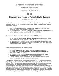
EE 658 Diagnosis and Design of Reliable Digital Systems (3, Fa)<br />
Fault models; test gener<strong>at</strong>ion; fault simul<strong>at</strong>ion; self-checking and self-testing<br />
circuits; design for testability; fault tolerant design techniques; case studies.<br />
Prerequisite: gradu<strong>at</strong>e standing.<br />
EE CAD I Overview of Computer-Aided Design for Digital <strong>VLSI</strong> Systems<br />
(4, Fa) Formerly EE680, labeled as EE599 for Fall 2010.<br />
Design flow and need, <strong>at</strong>tributes techniques associ<strong>at</strong>ed with CAD rel<strong>at</strong>ed<br />
problems, including verific<strong>at</strong>ion, high- (behavioral and register) and low-level<br />
(g<strong>at</strong>e) synthesis, partitioning, floor planning, placement and routing.<br />
Corequisite: EE 477.<br />
EE CAD II (EE581) Techniques and Models Used in Computer-Aided<br />
Design Tools for <strong>VLSI</strong> Circuits (3, Sp)<br />
M<strong>at</strong>hem<strong>at</strong>ical techniques employed in computer-aided-design systems,<br />
including: graph theory, algorithmic and heuristic techniques for combin<strong>at</strong>orial<br />
problems, d<strong>at</strong>a structures and modeling. Prerequisite: EE CAD I.<br />
EE CAD II Advanced topics in Computer-Aided Design for Digital <strong>VLSI</strong><br />
Systems (3, Fa) Formerly EE 681.<br />
An in-depth analysis of CAD techniques used for verific<strong>at</strong>ion, high- and lowlevel<br />
synthesis, floor planning, placement and routing, including unique<br />
aspects rel<strong>at</strong>ed to 3-D, power and clock distribution, and noise.<br />
Highly rel<strong>at</strong>ed digital systems courses<br />
EE 552 Asynchronous <strong>VLSI</strong> Design (3, FaSp)<br />
Asynchronous channels and architectures; implement<strong>at</strong>ion design styles;<br />
controller synthesis; hazards, and races; Petri-nets; performance analysis,<br />
and optimiz<strong>at</strong>ion; globally asynchronous locally synchronous design. Open<br />
only to gradu<strong>at</strong>e students. Prerequisite: EE 477.<br />
EE 560 Digital System Design-Tools and Techniques (3, Sm)<br />
ASIC design, FPGAs, VHDL, Verilog, test benches, simul<strong>at</strong>ion, synthesis,<br />
timing analysis, post-synthesis simul<strong>at</strong>ion, FIFOs, handshaking, memory<br />
interface, PCI bus protocol, CAD tools, design lab exercises. Prerequisite:<br />
EE 457, EE 454L; Recommended prepar<strong>at</strong>ion: familiarity with CAD tools.<br />
13<br />
Copyright 2010 M.A. Breuer
Highly rel<strong>at</strong>ed silicon rel<strong>at</strong>ed m<strong>at</strong>erials courses<br />
EE 480 Introduction to Nanoscience and Nanotechnology (3, Fa)<br />
Next-gener<strong>at</strong>ion nanoscale m<strong>at</strong>erials and electronic devices: nanoscale<br />
fabric<strong>at</strong>ion and characteriz<strong>at</strong>ion, nanom<strong>at</strong>erials, nanoelectronics, and<br />
nanobiotechnology. Prerequisite: EE 338.<br />
EE 504L Solid-St<strong>at</strong>e Processing and Integr<strong>at</strong>ed Circuits Labor<strong>at</strong>ory (3,<br />
Fa, Sp)<br />
Labor<strong>at</strong>ory oriented with lectures keyed to practical procedures and<br />
processes. Solid-st<strong>at</strong>e fabric<strong>at</strong>ion and analysis fundamentals; basic device<br />
construction techniques. Prerequisite: BSEE.<br />
EE 506 Semiconductor Physics (3)<br />
Semiconductor bonds, crystallography, band structure assumptions, group<br />
theory, band structure results, k.p. method, quantum wells, wires and dots,<br />
superl<strong>at</strong>tices, amorphous, organic semiconductors, defects, st<strong>at</strong>istics,<br />
surfaces. Prerequisite: MASC 501.<br />
Applic<strong>at</strong>ion areas<br />
EE 519 Speech Recognition and Processing for Multimedia (3, Fa)<br />
Speech production, acoustics, perception, synthesis, compression,<br />
recognition, transmission. Coding for speech, music, and CD-quality. Fe<strong>at</strong>ure<br />
extraction. Echo cancell<strong>at</strong>ion. Audio, visual synchroniz<strong>at</strong>ion. Multimedia,<br />
internet use. Prerequisite: EE 483.<br />
EE 483 Introduction to Digital Signal Processing (3, FaSp)<br />
Fundamentals of digital signal processing covering: discrete time linear<br />
systems, quantiz<strong>at</strong>ion, sampling, Z-transforms, Fourier transforms, FFTs and<br />
filter design. Prerequisite: EE 301.<br />
EE 567 Communic<strong>at</strong>ion Systems (3, Fa)<br />
Analysis of communic<strong>at</strong>ion systems oper<strong>at</strong>ing from very low to optical<br />
frequencies. Comparison of modul<strong>at</strong>ion and detection methods. System<br />
components description. Optimum design of communic<strong>at</strong>ion systems.<br />
Corequisite: EE 464 or EE 465; Recommended prepar<strong>at</strong>ion: EE 441.<br />
BME 451 Fundamentals of Biomedical Microdevices (3, Fa)<br />
BME 523 Measurement and Processing of Biological Signals (3, Fa)<br />
5. Text used in classes and for prepar<strong>at</strong>ion<br />
Prepar<strong>at</strong>ory: John Wakerly, Digital Design: Principles and Practices,<br />
Prentice Hall, Third or l<strong>at</strong>er edition. You must master almost all of the m<strong>at</strong>erial<br />
in this text before entering our program.<br />
Testing: Miron Abramovici, Melvin Breuer and Arthur Friedman, Digital<br />
Systems Testing and Testable Design, IEEE Press<br />
Testing: Niraj Jha and Sandeep Gupta, Testing Digital Systems, Cambridge<br />
University Press.<br />
CAD: Laung-Terng Wang (ed.), Electronic Design Autom<strong>at</strong>ion: Synthesis,<br />
Verific<strong>at</strong>ion, and Test, Morgan Kaufman.<br />
<strong>VLSI</strong>: Neil Weste and David Harris, CMOS <strong>VLSI</strong> Design: A Circuits and<br />
Systems Perspective, Addison-Wesley.<br />
14<br />
Copyright 2010 M.A. Breuer
<strong>VLSI</strong>: Peter A. Beerel, Recep O. Ozdag and Marcos Ferreti, A Designer’s<br />
Guide to Asynchronous <strong>VLSI</strong>, Cambridge University Press.<br />
6. Wh<strong>at</strong> are employers seeking?<br />
Below I have edited two calls for employment I received some time ago to give you an<br />
idea of wh<strong>at</strong> employers are looking for in a new employee in addition to good<br />
communic<strong>at</strong>ion and software skills. I have also reproduced an announcement about a<br />
new technology to illustr<strong>at</strong>e the dynamic n<strong>at</strong>ure of technology.<br />
• Advanced Technology Solutions for Automotive & Semi Conductor Industries<br />
An ever-growing range of cutting-edge technologies are emerging into<br />
production in the automotive electronic and semiconductor sectors. This<br />
makes these areas two of the most exciting and dynamic manufacturing<br />
sectors in the world.<br />
Today, Automotive & Semiconductor industries are facing a very difficult<br />
economic environment, together with heterogeneity increasing product<br />
quality, increased dependence on outsourcing, growing competition, and an<br />
endless list of business partners. The automotive electronics and<br />
semiconductor market sees enormous worldwide demand for its products,<br />
which brings tremendous opportunity for semiconductor companies. This<br />
increasing pressure to keep pace with the competition results in a reduction<br />
development time and the constant need for new and innov<strong>at</strong>ive products.<br />
However, not all products will do well in the marketplace as the consumer is<br />
extremely selective, and in particular on price and performance, leaving<br />
semiconductor companies deal with the triple challenges of increasing<br />
complexity, shorter lead times and growing competition. In fact, the need for<br />
enhancing quality, cre<strong>at</strong>ing product differenti<strong>at</strong>ion while meeting safety and<br />
other regul<strong>at</strong>ions, is becoming more challenging<br />
This kind of situ<strong>at</strong>ion has momentum for Advanced Technology Solutions,<br />
which provides solutions for the automotive and semiconductor industry to<br />
achieve the needed performance enhancements and improved efficiency.<br />
The partnership with our organiz<strong>at</strong>ion provides industry with the l<strong>at</strong>est<br />
technological solutions in the areas of: Automotive Electronics, Engineering<br />
Design, Product Engineering, car infotainment and telem<strong>at</strong>ics, instrument<br />
clusters, industrial autom<strong>at</strong>ion, drive, chip design, embedded software,<br />
Analog Mixed Signal Design, Electronic Design, Physical design,<br />
semiconductor design outsourcing, ASIC/SoC development, <strong>VLSI</strong> design,<br />
FPGA design solutions and support services such as Verific<strong>at</strong>ion &<br />
Valid<strong>at</strong>ion, offshore testing and automotive embedded software, a viable<br />
option as a lever on the technology know-how can the automotive industrial &<br />
semiconductor solutions. We also help in acceler<strong>at</strong>ing the development cycle<br />
and push the envelope of innov<strong>at</strong>ion.<br />
The use of this Advanced Technology Solutions, the automotive and<br />
semiconductor industries can work with a variety of business partners and<br />
suppliers in tandem to design and produce vehicles and focus on providing<br />
innov<strong>at</strong>ive working silicon chip design and embedded software support.<br />
15<br />
Copyright 2010 M.A. Breuer
• CN6194AL Bright Algorithm Development Engineer<br />
NEW positions with a commercial company based in Hertfordshire working on<br />
the design and license of silicon and software IP for today's multimedia and<br />
communic<strong>at</strong>ion devices.<br />
You'll have the opportunity to work on the next gener<strong>at</strong>ion of advanced<br />
graphics technology, and will become part of a dynamic, motiv<strong>at</strong>ed and very<br />
successful design team and organiz<strong>at</strong>ion.<br />
We are looking to recruit an academically bright gradu<strong>at</strong>e engineer or<br />
m<strong>at</strong>hem<strong>at</strong>ician with either a good degree, MSc or PhD and experience or a<br />
definite interest in gener<strong>at</strong>ing innov<strong>at</strong>ive implement<strong>at</strong>ions of m<strong>at</strong>hem<strong>at</strong>ical<br />
functions.<br />
Primarily we are looking for you to be responsible for:<br />
• research into cutting edge techniques for adders/multipliers &<br />
algebraic m<strong>at</strong>hem<strong>at</strong>ical functions<br />
• coding of a tool to gener<strong>at</strong>e RTL/VHDL<br />
• block level specific<strong>at</strong>ion<br />
• verific<strong>at</strong>ion/synthesis<br />
Ideally you'll have a good degree and a strong m<strong>at</strong>hem<strong>at</strong>ical background, 1-3<br />
years in a rel<strong>at</strong>ed field either <strong>at</strong> university or in industry and software in C++.<br />
Additional experience of algorithm development, implement<strong>at</strong>ion of<br />
adders/multipliers, VHDL/Verilog/RTL or ASIC design tools would be gre<strong>at</strong>.<br />
In return the company is offering you the chance to be a part of their<br />
continuing success and join a small team who are influencing the progress of<br />
the whole organiz<strong>at</strong>ion.<br />
• Finally, below I give you an example of a forthcoming technology, which<br />
demonstr<strong>at</strong>es why this industry is so dynamic and why we are continually<br />
developing new tools for synthesis and analysis.<br />
EE Times<br />
06/18/2010<br />
SAN JOSE, Calif. -- Grandis Inc. has been awarded $8.6 million from the<br />
Defense Advanced Research Projects Agency (Darpa) for the second phase<br />
of a research project developing spin-transfer torque random access memory<br />
(STT-RAM) chips.<br />
16<br />
Copyright 2010 M.A. Breuer
STT-RAM is a next-gener<strong>at</strong>ion, MRAM technology. The first phase, supported by<br />
an award amount of $6.0 million, began in 2008 and was scheduled to last two<br />
years.<br />
The program is being carried out by collabor<strong>at</strong>ion between Grandis, the<br />
Universities of Virginia and Alabama, and the College of William and Mary. The<br />
N<strong>at</strong>ional Institute of Standards and Technology and the Naval Research<br />
Labor<strong>at</strong>ory have provided additional support.<br />
The contract has covered STT-RAM m<strong>at</strong>erials and processes, as well as STT-<br />
RAM architecture and circuit blocks. During Phase II, work will include test and<br />
verific<strong>at</strong>ion of STT-RAM integr<strong>at</strong>ed memory arrays.<br />
“STT-RAM has huge potential as the only non-vol<strong>at</strong>ile Random Access memory<br />
which scales beyond 10-nm. It is also the only technology fast enough to replace<br />
the existing DRAMs. It can replace embedded SRAM and flash <strong>at</strong> 45-nm, DRAM<br />
<strong>at</strong> 32-nm, and ultim<strong>at</strong>ely can replace NAND,’’ st<strong>at</strong>ed Farhad Tabrizi, CEO and<br />
president of Grandis (Milpitas, Calif.), in a st<strong>at</strong>ement.<br />
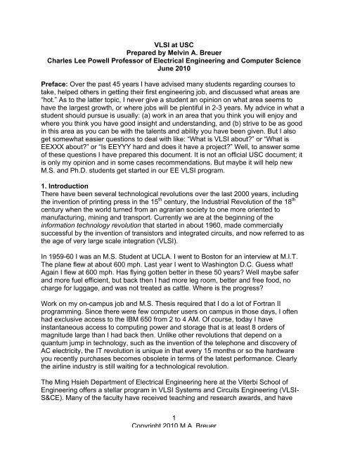
Testing<br />
Physical design<br />
A Designer must be able to do it all<br />
17<br />
Copyright 2010 M.A. Breuer<br />
Valid<strong>at</strong>ion<br />
Synthesis