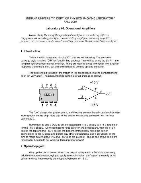
LM741 1 2 2 3 3 4 8 7 7 +15 V 15 V 4 6 6out 5 + - Indiana University
LM741 1 2 2 3 3 4 8 7 7 +15 V 15 V 4 6 6out 5 + - Indiana University
LM741 1 2 2 3 3 4 8 7 7 +15 V 15 V 4 6 6out 5 + - Indiana University

Create successful ePaper yourself
Turn your PDF publications into a flip-book with our unique Google optimized e-Paper software.
INDIANA UNIVERSITY, DEPT. OF PHYSICS, P400/540 LABORATORY<br />
FALL 2008<br />
Laboratory #6: Operational Amplifiers<br />
Goal: Study the use of the operational amplifier in a number of different<br />
configurations: inverting amplifier, non-inverting amplifier, summing amplifier,<br />
follower, current source, and current to voltage converter (transconductance amplifier)<br />
1. Introduction<br />
This is the first integrated circuit ("IC") that we will be using. The particular<br />
package style is called "DIP" for "dual in-line package." We will be using the <strong>LM741</strong>, the<br />
"original" low-cost operational amplifier. There are now op amps with lower noise, faster<br />
response ("slewing"), etc., but this one illustrates generic op amp behavior.<br />
The chip should "straddle" the trench in the breadboard, making connections to<br />
each pin very easy. The pin numbering scheme for all chips is as shown:<br />
8 7<br />
<strong>LM741</strong><br />
1 2<br />
6<br />
5<br />
3 4<br />
2<br />
3<br />
<strong>+<strong>15</strong></strong> V<br />
7<br />
4<br />
!<strong>15</strong> V<br />
The "dot" always designates pin 1, and the pins are numbered counter-clockwise<br />
looking down on the chip. Note that in the above, not all pins are used ("NC" or "not<br />
connected").<br />
Remember to use a DVM to set the adjustable <strong>+<strong>15</strong></strong> V supply to <strong>+<strong>15</strong></strong> V and ditto<br />
for the –<strong>15</strong> V supply. Connect these to "bus bars" on the breadboard, with the <strong>+<strong>15</strong></strong> V<br />
across the top and the –<strong>15</strong> V across the bottom. Immediately make the power<br />
connections to the IC chip, and before any other connections, use a DVM right at the<br />
pins to make sure that the <strong>+<strong>15</strong></strong> and –<strong>15</strong> Volts are present. This is one of the dominant<br />
reasons for IC circuits not working: lack of proper power!<br />
2. Open-loop gain<br />
Wire up the circuit below. Watch the output voltage with a DVM as you slowly<br />
twiddle the potentiometer, trying to apply zero volts (when the "wiper" is exactly at the<br />
center and you have exactly the midpoint between +/–<strong>15</strong> V).<br />
!<br />
+<br />
6<br />
out
Describe the behavior. Is it consistent with gain claims of "100's of volts/mV'?<br />
3. Inverting Amplifier<br />
10k<br />
in<br />
<strong>+<strong>15</strong></strong> V<br />
!<strong>15</strong> V<br />
1k<br />
2<br />
<strong>+<strong>15</strong></strong> V<br />
3<br />
+<br />
<strong>LM741</strong><br />
7<br />
2<br />
! 4<br />
10k<br />
<strong>LM741</strong><br />
3<br />
+<br />
!<strong>15</strong> V<br />
Construct the inverting amplifier drawn above. Drive the amplifier with a 1 kHz<br />
sine wave. Measure the gain? What is the maximum output swing? How about linearity<br />
(try a triangle wave)? Try sine waves of different frequencies. At some high frequency,<br />
the amplifier fails to work well. Figure out a way to estimate the slew rate, i.e., the fastest<br />
"slope" in V/ms or V/ns to which the amplifier can respond (N.B. if your signal is<br />
Asin(2πft), differentiating this once gives the slope of the signal (in volts per unit time) for<br />
any time, and you should be able to find the maximum slope. Alternatively, try inputting a<br />
square wave and see how the device tries to duplicate the "infinite" input slope.).<br />
Drive the circuit with a sine wave at 1 kHz again. Measure the input impedance of<br />
this amplifier circuit by adding a 1 kΩ resistor in series with the input.<br />
!<br />
6<br />
6<br />
out<br />
out
4. Summing Amplifier<br />
in<br />
10k<br />
<strong>15</strong>k<br />
10k<br />
<strong>+<strong>15</strong></strong> V !<strong>15</strong> V<br />
Adjustable<br />
"DC Offset"<br />
2<br />
10k<br />
<strong>LM741</strong><br />
3<br />
+<br />
Let's get the "operational" of the operational amplifier: adding signals (currents<br />
really): Build the circuit above that allows you to sum a DC level with an input signal. For<br />
the input, choose a small amplitude sine wave. Describe its operation and the range of<br />
DC offsets you were able to achieve.<br />
5. Non-inverting Amplifier<br />
Wire up the non-inverting amplifier below. Measure the voltage gain and compare<br />
it to prediction.<br />
Try to measure the circuit's input impedance, at 1 kHz, by putting a 1 Meg<br />
resistor in series with the input. How is this different from the inverting amplifier?<br />
in<br />
1k<br />
3<br />
2<br />
+<br />
<strong>LM741</strong><br />
!<br />
10k<br />
!<br />
6<br />
6<br />
out<br />
out
6. Follower<br />
in<br />
3 +<br />
2<br />
<strong>LM741</strong><br />
Build the follower shown above. Input a sine wave of some frequency and<br />
examine the output and measure the gain. The ultimate boring circuit! What is it good<br />
for?<br />
Different Op Amp Uses<br />
Because they can accept either voltages or currents as inputs, and produce voltage<br />
or current outputs, we can label amplifiers as one four types:<br />
!<br />
6<br />
out<br />
Input Output Amplifier Name<br />
Voltage Voltage Voltage<br />
Voltage Current Transconductance<br />
Current Voltage Transresistance<br />
Current Current Current<br />
In the next section, you will construct a current source that is controlled by an input<br />
voltage (a "transconductance" amplifier). It is similar to the non-inverting amplifier, with<br />
the input voltage set with a voltage divider.
7. Current Source<br />
<strong>15</strong>k<br />
1k<br />
<strong>+<strong>15</strong></strong> V<br />
180<br />
3<br />
2<br />
+<br />
<strong>LM741</strong><br />
!<br />
A<br />
6<br />
10k "load"<br />
Try out the op-amp current source shown above. What should the current be,<br />
and what do you measure it as? Vary the load potentiometer and watch the current using<br />
the DVM. Determine the range of load resistances over which the current source varies<br />
by less than 10%. This is called its compliance.<br />
This current source, although far more precise and stable than our simple<br />
transistor current source, has the disadvantage of requiring a "floating" load (neither side<br />
connected to ground). It also has significant speed limitations when the output current or<br />
load impedance varies at microsecond speeds.<br />
8. Current to Voltage Converter<br />
Phototransistor<br />
(no collector<br />
connection)<br />
light<br />
2<br />
"<br />
3 +<br />
<strong>LM741</strong><br />
10 M!<br />
6<br />
out<br />
out
(a) Photodiode: Use the supplied phototransistor (feel free to peel back some of<br />
the rubber coating if not enough light is getting into the fiber optic lead) as a photodiode<br />
in the circuit above. To determine the pins, try using the DVM to distinguish them as<br />
learned previously. Examine the output signal (if the DC level is more than 10 V, reduce<br />
the feedback resistor to 1 MΩ).<br />
If you see fuzz on the output (oscillations), put a small capacitor (~100 pF) in<br />
parallel with the feedback resistor.<br />
What is the average DC output level, and what is the percentage "modulation"?<br />
This can be quite large due to the fluorescent lights in the lab... What input photocurrent<br />
does the output level correspond to? Try covering the phototransistor with your hand.<br />
Look at the "summing junction" (the inverting input pin) with the scope, as the output<br />
voltage varies. What should you see?<br />
(b) Phototransistor: Now connect the device as a phototransistor, as shown<br />
below (the base is to be left open, as shown). What is the average input photocurrent<br />
now? What about the percentage modulation? Look again at the summing junction.<br />
light<br />
<strong>+<strong>15</strong></strong> V<br />
Phototransistor<br />
2<br />
<strong>LM741</strong><br />
3<br />
+<br />
100k (or more)<br />
If you are curious and/or interested, try out the "game" on pg. 182 of your<br />
manual!<br />
!<br />
6<br />
out