Novel Power MOSFET Packaging Technology Doubles Power ...
Novel Power MOSFET Packaging Technology Doubles Power ...
Novel Power MOSFET Packaging Technology Doubles Power ...

Create successful ePaper yourself
Turn your PDF publications into a flip-book with our unique Google optimized e-Paper software.
3. Facilitate simplified board layout and<br />
paralleling of devices.<br />
4. Enable the use of existing surface mount<br />
assembly lines and technology.<br />
In order to achieve points 1 and 2 above, the<br />
design of DirectFET technology has rationalised some<br />
of the concepts and materials that are commonly used in<br />
power packaging. This simplified approach is shown as a<br />
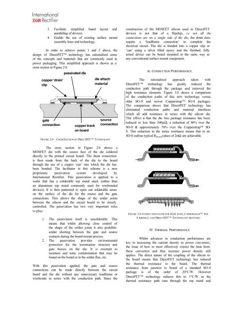
cross section in Figure 2.0.<br />
copper ‘drain’<br />
clip<br />
gate<br />
connection<br />
passivated die<br />
copper track<br />
on board<br />
die attach<br />
material<br />
source<br />
connection<br />
FIGURE 2.0 – CROSS SECTION OF DIRECTFET TECHNOLOGY<br />
The cross section in Figure 2.0 shows a<br />
<strong>MOSFET</strong> die with the source face of the die soldered<br />
directly to the printed circuit board. The drain connection<br />
is then made from the back of the die to the board<br />
through the use of a copper ‘can’ into which the die has<br />
been bonded. The facilitator in this scheme is a new<br />
proprietary passivation system developed by<br />
International Rectifier. This passivation is applied to a<br />
wafer that has a solderable top metal stack (rather than<br />
an aluminium top metal commonly used for wirebonded<br />
devices). It is then patterned to open out solderable areas<br />
on the surface of the die for the source and the gate<br />
connections. This allows the shape of the solder joints<br />
between the silicon and the circuit board to be closely<br />
controlled. The passivation has two very important roles<br />
to play:<br />
1. The passivation itself is unsolderable. This<br />
means that whilst allowing close control of<br />
the shape of the solder joints it also prohibits<br />
solder shorting between the gate and source<br />
contacts during the board mount process.<br />
2. The passivation provides environmental<br />
protection for the termination structure and<br />
gate busses on the die. It is resistant to<br />
moisture and ionic contamination that may be<br />
found on the board or in the solder flux, etc.<br />
With this passivation applied, the gate and source<br />
connections can be made directly between the circuit<br />
board and the die without any unnecessary leadframe or<br />
wirebonds in series with the conduction path. Since the<br />
construction of the <strong>MOSFET</strong> silicon used in DirectFET<br />
devices is not that of a flipchip, i.e not all the<br />
connections are on a single side of the die, the drain does<br />
require a ‘leadframe connection’ to complete the<br />
electrical circuit. The die is bonded into a copper clip or<br />
‘can’ using a silver filled epoxy and the finished, fully<br />
tested device can be board mounted in the same way as<br />
any conventional surface mount component.<br />
III. CONDUCTION PERFORMANCE<br />
The rationalised approach taken with<br />
DirectFET technology has greatly reduced the<br />
conduction path through the package and removed the<br />
high resistance elements. Figure 3.0 shows a comparison<br />
of the conduction paths of this new technology versus<br />
older SO -8 and newer Copperstrap SO-8 packages.<br />
The comparison shows that DirectFET technology has<br />
eliminated conduction paths and material interfaces<br />
which all add resistance in series with the silicon die.<br />
The effect is that the die free package resistance has been<br />
reduced to less than 200μΩ, a reduction of 86% over the<br />
SO-8 & approximately 74% over the Copperstrap SO-<br />
8. This reduction in the series resistance means that in an<br />
SO-8 outline typical R ds(on)values of 2mΩ are achievable.<br />
FIGURE 3.0 CONDUCTION PATHS FOR SO-8 (TOP), COPPERSTRAP SO-<br />
8 (MIDDLE) AND DIRECTFET TECHNOLOGY (BOTTOM)<br />
IV. THERMAL PERFORMANCE<br />
Whilst advances in conduction performance are<br />
key to increasing the current density in power converters,<br />
the issue of how to most effectively extract the heat from<br />
these converters and thus increase power density still<br />
applies. The direct nature of the coupling of the silicon to<br />
the board means that DirectFET technology has reduced<br />
the thermal resistance to the board. The thermal<br />
resistance from junction to board of a standard SO-8<br />
package is of the order of 20°C/W. However<br />
DirectFET technology reduces this to 1°C/W as the<br />
thermal resistance path runs through the top metal and