Stepper Motor Control Using the PIC16F684 - Microchip
Stepper Motor Control Using the PIC16F684 - Microchip
Stepper Motor Control Using the PIC16F684 - Microchip

You also want an ePaper? Increase the reach of your titles
YUMPU automatically turns print PDFs into web optimized ePapers that Google loves.
Author: Reston Condit<br />
<strong>Microchip</strong> Technology Inc.<br />
INTRODUCTION<br />
This application note will describe how to drive a<br />
bipolar stepping motor with <strong>the</strong> <strong>PIC16F684</strong>. The<br />
<strong>PIC16F684</strong> has an ideal set of peripherals for driving a<br />
stepper motor. These peripherals include two on-chip<br />
comparators and an Enhanced Capture Compare<br />
PWM (ECCP) module. The ECCP module is used to<br />
microstep <strong>the</strong> motor while <strong>the</strong> on-chip comparators limit<br />
<strong>the</strong> current in <strong>the</strong> windings of <strong>the</strong> motor.<br />
Note: Please refer to AN907: Stepping <strong>Motor</strong><br />
Fundamentals for information on <strong>the</strong> types<br />
of stepper motors, microstepping and<br />
current limiting techniques.<br />
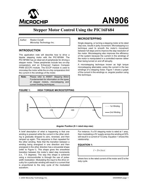
FIGURE 1: HIGH TORQUE MICROSTEPPING<br />
Current<br />
<strong>Stepper</strong> <strong>Motor</strong> <strong>Control</strong> <strong>Using</strong> <strong>the</strong> <strong>PIC16F684</strong><br />
A brief description of what is happening is that one<br />
winding is powered while <strong>the</strong> current in <strong>the</strong> o<strong>the</strong>r winding<br />
is gradually dropped to zero, reversed, and <strong>the</strong>n<br />
ramped up again. This sequence is <strong>the</strong>n repeated for<br />
<strong>the</strong> o<strong>the</strong>r winding. Note that <strong>the</strong> transition between a<br />
winding being energized in one direction and <strong>the</strong>n<br />
energized in <strong>the</strong> o<strong>the</strong>r direction has a sinusoidal shape<br />
(refer to Figure 1). This shape gives <strong>the</strong> smoo<strong>the</strong>st<br />
transition between <strong>the</strong> motor’s rated step increments<br />
(i.e., 7.5 degrees). The way this shape is achieved<br />
using a microcontroller is through <strong>the</strong> use of pulsewidth<br />
modulation. Modulating <strong>the</strong> input to <strong>the</strong> drive circuitry<br />
for a particular winding will result in a current that<br />
is proportional to <strong>the</strong> duty cycle of <strong>the</strong> modulated<br />
waveform.<br />
MICROSTEPPING<br />
+3S +6S +9S<br />
Angular Position (S = rated step size)<br />
AN906<br />
Single stepping, or turning a stepping motor at its rated<br />
step size, results in jerky movement. Microstepping is a<br />
technique used to smooth <strong>the</strong> motor’s movement<br />
between full steps and to improve <strong>the</strong> step resolution of<br />
<strong>the</strong> motor. Microstepping also improves <strong>the</strong> efficiency<br />
of <strong>the</strong> system because <strong>the</strong> current in <strong>the</strong> windings of<br />
<strong>the</strong> motor is manipulated in a controlled manner ra<strong>the</strong>r<br />
than being turned on and off abruptly.<br />
A microstepping technique known as high torque<br />
microstepping alternately varies <strong>the</strong> current in <strong>the</strong> two<br />
windings of a stepping motor. Figure 1 shows a graph<br />
of <strong>the</strong> current in <strong>the</strong> windings vs. angular position using<br />
this technique.<br />
For instance, if a 5V stepping motor is rated at 1 amp,<br />
<strong>the</strong>n modulating a 5V supply across <strong>the</strong> winding at 50%<br />
will result in a current of 1/2 amp. Equation 1 shows this<br />
relationship:<br />
EQUATION 1:<br />
I = D× IMAX<br />
1st Winding<br />
2nd Winding<br />
where IMAX is <strong>the</strong> rated current of <strong>the</strong> motor and D is <strong>the</strong><br />
duty cycle.<br />
© 2004 <strong>Microchip</strong> Technology Inc. DS00906A-page 1
AN906<br />
In order to achieve <strong>the</strong> sinusoidal transition from a<br />
positive to negative charge in a winding, numerous<br />
microsteps are needed. The number of microsteps<br />
typically ranges from 4 to 32 microsteps per rated step<br />
size. Ra<strong>the</strong>r than calculating <strong>the</strong> duty cycle for a particular<br />
microstep on <strong>the</strong> fly, a duty cycle look-up table is<br />
implemented in firmware. The number of table values<br />
is equal to <strong>the</strong> number of steps desired for a particular<br />
microstepping sequence. Equation 2 is used to obtain<br />
<strong>the</strong> duty cycle values for <strong>the</strong> top half of <strong>the</strong> table. The<br />
second half of <strong>the</strong> table is simply <strong>the</strong> top half in reverse<br />
order.<br />
EQUATION 2:<br />
D(step number) = cos((step number×Π)/((number of<br />
steps)+1)) × ((2^bits resolution)-1)<br />
<strong>Using</strong> Equation 2 <strong>the</strong> following duty cycle values were<br />
calculated for a 16 microsteps per full step sequence<br />
using an 8-bit resolution PWM waveform:<br />
TABLE 1: DUTY CYCLE VALUES FOR<br />
MICROSTEPPING<br />
Step<br />
Number<br />
D<br />
Step<br />
Number<br />
1 251 9 44<br />
2 240 10 87<br />
3 221 11 128<br />
4 195 12 164<br />
5 164 13 195<br />
6 128 14 221<br />
7 87 15 240<br />
8 44 16 251<br />
D<br />
PWM Generation <strong>Using</strong> <strong>the</strong> ECCP Module<br />
The ECCP module on <strong>the</strong> <strong>PIC16F684</strong> is ideal for<br />
generating <strong>the</strong> PWM signal required for microstepping.<br />
The module is capable of generating a 10-bit resolution<br />
PWM waveform at frequencies ranging up to 7.81 kHz<br />
when using <strong>the</strong> microcontroller’s 8 MHz internal oscillator.<br />
Higher frequencies are possible, but at <strong>the</strong> cost of<br />
PWM resolution.<br />
The ECCP module has four modes of operation:<br />
1) Single output<br />
2) Half-bridge output<br />
3) Full-bridge forward output<br />
4) Full-bridge reverse output<br />
In half-bridge mode <strong>the</strong> module modulates two pins<br />
simultaneously, pins P1A and P1B. For this application,<br />
<strong>the</strong>se two outputs are used to drive <strong>the</strong> two windings of<br />
a stepping motor. The following circuit diagram shows<br />
how <strong>the</strong>se pins are connected to a bipolar drive circuit.<br />
DS00906A-page 2 © 2004 <strong>Microchip</strong> Technology Inc.
FIGURE 2: BIPOLAR DRIVE CIRCUIT<br />
P1A<br />
CTRLA1<br />
VSUPPLY<br />
VSUPPLY<br />
R1<br />
10K<br />
VSUPPLY<br />
VSUPPLY<br />
Winding 1<br />
P1B<br />
CTRLB1<br />
Winding 2<br />
CTRLB2<br />
AN906<br />
CTRLA2<br />
© 2004 <strong>Microchip</strong> Technology Inc. DS00906A-page 3
AN906<br />
Note <strong>the</strong> pull-up resistor on pins P1A and P1B. These<br />
resistors clamp <strong>the</strong> respective line high when <strong>the</strong> pin is<br />
tristated. It is important that <strong>the</strong> non-modulated line be<br />
clamped high so that <strong>the</strong> NAND gates on ei<strong>the</strong>r end of<br />
<strong>the</strong> winding can drive current through <strong>the</strong> winding when<br />
<strong>the</strong> respective control line is enabled.<br />
TABLE 2: WINDING STATES<br />
* Pin is tristated and <strong>the</strong> pull-up resistor is clamping <strong>the</strong><br />
line high.<br />
In States 0, 2, 4 and 6 <strong>the</strong> first half of <strong>the</strong> duty cycle sine<br />
look-up table (decreasing values) is referenced. In<br />
States 1, 3, 5 and 7 <strong>the</strong> second half of <strong>the</strong> duty cycle<br />
sine look-up table (increasing values) is referenced.<br />
CURRENT LIMITING<br />
Current limiting is used when a stepping motor is driven<br />
at a voltage that is higher than <strong>the</strong> motor’s rated<br />
voltage. There are several advantages to driving a<br />
motor at high voltage, namely, <strong>the</strong> torque and speed<br />
characteristics of <strong>the</strong> motor are improved. These<br />
parameters are improved because <strong>the</strong> current in <strong>the</strong><br />
motor windings is more responsive to changes made<br />
by <strong>the</strong> controller.<br />
When running a motor at a voltage that is higher than<br />
its rated voltage, current limiting considerations must<br />
be made. The current in <strong>the</strong> windings of <strong>the</strong> motor can<br />
not exceed <strong>the</strong> maximum current rating of <strong>the</strong> motor or<br />
motor life will be severely affected. One of <strong>the</strong> most<br />
effective ways to limit current is through <strong>the</strong> use of a<br />
chopper circuit. The chopper circuit for one winding is<br />
shown in Figure 3. Winding 2 uses <strong>the</strong> second on-chip<br />
comparator in its chopper circuit.<br />
The ECCP module is set up so that <strong>the</strong> waveforms on<br />
pins P1A and P1B are identical. This is done by configuring<br />
<strong>the</strong> CCP1CON register so that P1A is active high<br />
and P1B is active low. With no dead band delay <strong>the</strong>se<br />
pins will behave identically. Configuring <strong>the</strong> module in<br />
this way enables each winding control block to use <strong>the</strong><br />
same duty cycle look-up table values for it’s transition<br />
sequence. The following table shows all eight winding<br />
states.<br />
STATE 0 1 2 3 4 5 6 7<br />
Winding 1<br />
Polarity<br />
+ to 0 0 to - - - - to 0 0 to + + +<br />
Winding 2<br />
Polarity<br />
+ + + to 0 0 to - - - - to 0 0 to +<br />
P1A Duty Cycle 100% to 0 0 to 100% 100%* 100%* 100% to 0 0 to 100% 100%* 100%*<br />
P1B Duty Cycle 100%* 100%* 100% to 0 0 to 100% 100%* 100%* 100% to 0 0 to 100%<br />
TRISC, P1A 0 0 1 1 0 0 1 1<br />
TRISC, P1B 1 1 0 0 1 1 0 0<br />
CTRL1A 1 0 0 0 0 1 1 1<br />
CTRL1B 0 1 1 1 1 0 0 0<br />
CTRL2A 1 1 1 0 0 0 0 1<br />
CTRL2B 0 0 0 1 1 1 1 0<br />
DS00906A-page 4 © 2004 <strong>Microchip</strong> Technology Inc.
FIGURE 3: BIPOLAR STEPPING MOTOR DRIVE CIRCUIT WITH CHOPPER CONTROL<br />
P1A<br />
CTRLA1<br />
VSUPPLY<br />
R1<br />
10K<br />
C1OUT<br />
VSUPPLY<br />
Winding 1<br />
VCTRL<br />
AN906<br />
© 2004 <strong>Microchip</strong> Technology Inc. DS00906A-page 5<br />
C1IN+<br />
C1IN-<br />
CTRLA2
AN906<br />
An over current condition is detected by comparing <strong>the</strong><br />
voltage measured across RSENSE (VSENSE) to a control<br />
voltage (VCONTROL). The maximum voltage VSENSE<br />
should be allowed to reach is determined by:<br />
EQUATION 3:<br />
VCONTROL is set so that it is equal to VSENSE when IMAX<br />
is reached. A simple voltage divider is used to create<br />
VCONTROL where <strong>the</strong> values of R1 and R2 are chosen<br />
to satisfy <strong>the</strong> following equation:<br />
EQUATION 4:<br />
RSENSE is chosen arbitrarily, however, <strong>the</strong> smaller<br />
RSENSE is <strong>the</strong> more efficient <strong>the</strong> circuit. If RSENSE is too<br />
small <strong>the</strong>n VSENSE will be very small and <strong>the</strong> comparator<br />
output will be more sensitive to noise. The power<br />
dissipation of RSENSE was determined by:<br />
EQUATION 5:<br />
When <strong>the</strong> comparator indicates that IMAX has been<br />
reached, <strong>the</strong> control lines are forced low for <strong>the</strong> respective<br />
winding. This is done in firmware.<br />
It is only necessary to detect over-current in <strong>the</strong> winding<br />
that is not being modulated. For example, this<br />
would be states 2, 3, 6 and 7 for winding 1 (refer to<br />
Table 2). Current in <strong>the</strong> winding that is being modulated<br />
is controlled by limiting <strong>the</strong> maximum duty cycle of <strong>the</strong><br />
PWM waveform. This requires a modification to <strong>the</strong><br />
duty cycle sine look-up table talked about in <strong>the</strong><br />
previous section. The table is modified according to <strong>the</strong><br />
following relation:<br />
EQUATION 6:<br />
VSENSE = RSENSE × IMAX<br />
VCONTROL = (R1/(R1+R2))VCC<br />
P = IMAX 2 RSENSE<br />
D(step number) =<br />
Dx(step number) × VMAX/VSUPPLY<br />
where VMAX is <strong>the</strong> rated voltage of <strong>the</strong> motor and Dx is<br />
<strong>the</strong> array of duty cycle values calculated using<br />
Equation 2 from <strong>the</strong> previous section.<br />
EXAMPLE APPLICATION<br />
This example application demonstrates how to drive a<br />
1.8 degree-per-step stepping motor. The motor used is<br />
a bipolar stepping motor rated to draw 1/2 amp at 5V.<br />
For this example, <strong>the</strong> motor is driven at 12V or 2.4<br />
times <strong>the</strong> motor’s rated voltage.<br />
Hardware<br />
Appendix A shows a schematic for <strong>the</strong> example<br />
application included with this application note. The drive<br />
circuit is composed of four Fairchild Semiconductor<br />
half-bridge MOSFET ICs (part number FDC6420C).<br />
These ICs are tied to ground via a 1 ohm, 1/2 W<br />
resistor. The value of RSENSE was chosen using<br />
Equation 1 so that VSENSE will be equal to 0.5V when<br />
IMAX is reached. <strong>Using</strong> Equation 3, <strong>the</strong> power<br />
dissipated by RSENSE is 1/4 W, <strong>the</strong>refore, a 1/2 W<br />
resistor is sufficient.<br />
Two <strong>Microchip</strong> logic-input CMOS quad drivers are<br />
used to drive <strong>the</strong> MOSFET ICs and to provide <strong>the</strong> logic<br />
necessary for <strong>the</strong> implementation described in this<br />
application note. The TC4467 has four on-chip NAND<br />
gates and <strong>the</strong> TC4468 has four on-chip AND gates.<br />
The inputs to each of <strong>the</strong> AND gates on <strong>the</strong> TC4468<br />
are tied toge<strong>the</strong>r because this IC is used as a noninverting<br />
quad MOSFET driver for this implementation.<br />
Resistors R17 and R13 were chosen so that VCONTROL<br />
equals approximately 0.5 volts. R17 is 10 kOhm and<br />
R13 is 90.0 kOhm.<br />
Firmware<br />
A flowchart illustrating <strong>the</strong> firmware implementation of<br />
this example is in Appendix B. The source code for this<br />
application note is written in <strong>the</strong> <strong>Microchip</strong> assembly<br />
language and is included with this application note on<br />
<strong>Microchip</strong>’s web site, www.microchip.com.<br />
Operation<br />
The speed of <strong>the</strong> motor is adjusted using a potentiometer<br />
(R18). The motor is started and stopped via Switch<br />
1. There are four modes of operation in <strong>the</strong> example<br />
that are sequenced through with single button presses.<br />
The modes of operation are off, forward, off, and<br />
reverse.<br />
DS00906A-page 6 © 2004 <strong>Microchip</strong> Technology Inc.
CONCLUSION<br />
The <strong>PIC16F684</strong> has an ideal set of peripherals for lowcost<br />
stepping motor control. The ECCP module can be<br />
configured for microstepping applications while <strong>the</strong> two<br />
on-chip comparators can be configured to provide<br />
current feedback for current limiting applications. Extra<br />
I/O pins and CPU resources are left over for<br />
implementing serial communication, an LCD interface,<br />
or any number of I/O configurations.<br />
REFERENCES<br />
AN907: <strong>Stepper</strong> <strong>Motor</strong> Fundamentals<br />
AN906<br />
© 2004 <strong>Microchip</strong> Technology Inc. DS00906A-page 7
AN906<br />
DS00906A-page 8 © 2004 <strong>Microchip</strong> Technology Inc.<br />
APPENDIX A:<br />
<strong>PIC16F684</strong><br />
TC4467<br />
+5V<br />
R20<br />
10K<br />
C16<br />
0.1 uF<br />
R10<br />
100R<br />
S1<br />
SW-B3F1000<br />
+5V<br />
+5V<br />
+5V<br />
1<br />
2<br />
3<br />
4<br />
5<br />
6<br />
7<br />
RA5<br />
RA4<br />
P1A<br />
P1B<br />
RC3<br />
U1<br />
VDD<br />
RA5<br />
RA4<br />
RC5<br />
RC4<br />
RC3<br />
RA3/MCLR<br />
GND<br />
RA0<br />
RA1<br />
RA2<br />
RC0<br />
RC1<br />
RC2<br />
14<br />
13<br />
12<br />
11<br />
10<br />
9<br />
8<br />
C1IN+<br />
C1IN-<br />
AN2<br />
C2IN-<br />
C2IN+<br />
RC2<br />
+5V<br />
+5V<br />
R3<br />
10K<br />
U2<br />
P1A<br />
R2<br />
10K<br />
P1B<br />
1<br />
2<br />
3<br />
4<br />
5<br />
6<br />
8<br />
9<br />
14<br />
13<br />
12<br />
11<br />
10<br />
7<br />
1A<br />
1B<br />
2A<br />
2B<br />
3A<br />
3B<br />
4A<br />
4B<br />
VDD<br />
1Y<br />
2Y<br />
3Y<br />
4Y<br />
GND<br />
U3<br />
VSUPPLY<br />
TC4468<br />
1<br />
2<br />
3<br />
4<br />
5<br />
6<br />
8<br />
9<br />
14<br />
13<br />
12<br />
11<br />
10<br />
7<br />
1A<br />
1B<br />
2A<br />
2B<br />
3A<br />
3B<br />
4A<br />
4B<br />
VDD<br />
1Y<br />
2Y<br />
3Y<br />
4Y<br />
GND<br />
10K R6<br />
RC2<br />
RA4<br />
AN2<br />
C1IN+<br />
R19<br />
100R<br />
CW<br />
CCW<br />
2<br />
3<br />
R13<br />
90.9K<br />
10K<br />
R17<br />
R18<br />
1K<br />
POT-3352E 1<br />
VSUPPLY<br />
2 2<br />
D3<br />
BAT54S 2<br />
2<br />
S2<br />
G2<br />
D2<br />
3<br />
S2<br />
G2<br />
D2<br />
3<br />
4<br />
4<br />
6<br />
6 Winding 1<br />
FDC6420C<br />
Q5:B<br />
Q3:A<br />
FDC6420C<br />
FDC6420C<br />
FDC6420C<br />
Q6:B<br />
Q4:A<br />
1<br />
1<br />
3<br />
3 BAT54S<br />
D4<br />
D1<br />
G1<br />
S1<br />
1<br />
5<br />
D1<br />
G1<br />
S1<br />
1<br />
5<br />
R14<br />
1<br />
C1IN-<br />
VSUPPLY<br />
D6<br />
BAT54S<br />
BAT54S<br />
D5<br />
2<br />
1<br />
3<br />
2<br />
1<br />
3<br />
Winding 1<br />
2<br />
S2<br />
3<br />
G2<br />
S2<br />
D2 FDC6420C<br />
Q8:B<br />
Q7:A<br />
FDC6420C<br />
4<br />
6<br />
1<br />
5<br />
D1<br />
G1<br />
S1<br />
2<br />
G2<br />
D2<br />
3<br />
4<br />
6<br />
FDC6420C<br />
Q10:B<br />
Q9:A<br />
FDC6420C D1<br />
1 G1<br />
S1<br />
5<br />
R15<br />
1<br />
C2IN-<br />
RA5<br />
R7<br />
10K<br />
10K R8<br />
R9<br />
10K<br />
RC3<br />
VSUPPLY
APPENDIX A: (CONTINUED)<br />
VSUPPLY<br />
J7<br />
DIN5P_RECEPTICAL<br />
3<br />
5<br />
6<br />
2<br />
4<br />
7<br />
1<br />
100 uF<br />
P5 P4 P3<br />
1<br />
1 RA5 1<br />
2<br />
2 RA4 2<br />
3<br />
3 VPP 3<br />
4<br />
4 RC5 4<br />
5<br />
5 RC4 5<br />
6<br />
6 RC3 6<br />
7<br />
7 ICSPDAT 7<br />
8<br />
8 ICSPCLK 8<br />
9<br />
9 RA2 9<br />
10<br />
10 RC0 10<br />
11<br />
11 RC1 11<br />
12<br />
12 RC2 12<br />
13<br />
13 13<br />
14<br />
14 14<br />
HDR1X14 HDR1X14 HDR1X14<br />
C11<br />
VSUPPLY<br />
U10<br />
LM78L05ACM<br />
1<br />
IN OUT<br />
GND GND GND GND<br />
2 3 6 7<br />
AN906<br />
© 2004 <strong>Microchip</strong> Technology Inc. DS00906A-page 9<br />
RA5<br />
RA4<br />
RA3<br />
P1A<br />
P1B<br />
RC3<br />
1 uF<br />
C2IN+<br />
C1IN-<br />
AN2<br />
C2IN+<br />
C2IN-<br />
RC2<br />
C12<br />
+5V<br />
0.1 uF<br />
C13 8<br />
C14 +5V<br />
0.1 uF
AN906<br />
APPENDIX B:<br />
Initialize<br />
Internal oscillator<br />
frequency = 8 MHz<br />
Assign I/O pins<br />
Setup ADC pin:<br />
AN2<br />
Setup ECCP Module:<br />
Half Bridge Mode,<br />
31.25 kHz waveform<br />
Set TMR0<br />
parameters<br />
Turn on Comparators<br />
Turn on TMR2<br />
goto Main<br />
DS00906A-page 10 © 2004 <strong>Microchip</strong> Technology Inc.
APPENDIX B: (CONTINUED)<br />
0<br />
Clear control lines:<br />
CTRLA1, CTRLA2,<br />
CTRLB1, CTRLB2<br />
goto Main<br />
Read Switch Sw1<br />
Button<br />
Press?<br />
Increment Mode<br />
AN906<br />
Set Direction Flag<br />
Clear control lines:<br />
CTRLA1, CTRLA2,<br />
CTRLB1, CTRLB2<br />
Clear Direction Flag<br />
goto<br />
<strong>Motor</strong>State<br />
No<br />
Main<br />
Mode?<br />
goto<br />
<strong>Motor</strong>State<br />
© 2004 <strong>Microchip</strong> Technology Inc. DS00906A-page 11<br />
Yes<br />
1 2<br />
goto Main<br />
Debounce Routine<br />
3
AN906<br />
APPENDIX B: (CONTINUED)<br />
<strong>Motor</strong>State<br />
TMR2<br />
Interrupt<br />
Flag Set?<br />
No<br />
Duty Cycle<br />
Lookup Table<br />
State?<br />
Yes<br />
No<br />
Clear TMR2<br />
Interrupt Flag<br />
Read Potentiometer<br />
Move high 4-bits of ADC<br />
value into TMR2 Prescaler<br />
Initiate next ADC read<br />
<strong>Motor</strong><br />
Direction?<br />
Read previous Duty<br />
Cycle value<br />
End/Middle<br />
of Lookup<br />
Table?<br />
Reverse<br />
Forward<br />
DS00906A-page 12 © 2004 <strong>Microchip</strong> Technology Inc.<br />
Yes<br />
R3<br />
Duty Cycle<br />
Lookup Table<br />
Read next Duty<br />
Cycle value<br />
Increment State<br />
0 1 2 3 4 5 6 7<br />
goto State0 goto State2 goto State4<br />
goto State6<br />
goto State1 goto State3 goto State5<br />
goto State7
APPENDIX B: (CONTINUED)<br />
No<br />
No<br />
State0<br />
Enable P1A<br />
Disable P1B<br />
CTRLA1 = 0<br />
CTRLA2 = 0<br />
CTRLB1 = 1<br />
CTRLB2 = 1<br />
Imax Reached?<br />
Yes<br />
CTRLBx = 0<br />
goto Main<br />
State4<br />
Enable P1A<br />
Disable P1B<br />
CTRLA1 = 0<br />
CTRLA2 = 1<br />
CTRLB1 = 0<br />
CTRLB2 = 1<br />
Imax Reached?<br />
Yes<br />
CTRLBx = 0<br />
goto Main<br />
No<br />
No<br />
State1<br />
Enable P1A<br />
Disable P1B<br />
CTRLA1 = 0<br />
CTRLA2 = 1<br />
CTRLB1 = 1<br />
CTRLB2 = 0<br />
Imax Reached?<br />
Yes<br />
CTRLBx = 0<br />
goto Main<br />
State5<br />
Enable P1A<br />
Disable P1B<br />
CTRLA1 = 1<br />
CTRLA2 = 0<br />
CTRLB1 = 0<br />
CTRLB2 = 1<br />
Imax Reached?<br />
Yes<br />
CTRLBx = 0<br />
goto Main<br />
State2<br />
Disable P1A<br />
Enable P1B<br />
CTRLA1 = 0<br />
CTRLA2 = 0<br />
CTRLB1 = 1<br />
CTRLB2 = 1<br />
Imax Reached?<br />
CTRLAx = 0<br />
goto Main<br />
AN906<br />
© 2004 <strong>Microchip</strong> Technology Inc. DS00906A-page 13<br />
No<br />
No<br />
Yes<br />
State6<br />
Disable P1A<br />
Enable P1B<br />
CTRLA1 = 1<br />
CTRLA2 = 0<br />
CTRLB1 = 0<br />
CTRLB2 = 1<br />
Imax Reached?<br />
Yes<br />
CTRLAx = 0<br />
goto Main<br />
No<br />
No<br />
State3<br />
Disable P1A<br />
Enable P1B<br />
CTRLA1 = 0<br />
CTRLA2 = 1<br />
CTRLB1 = 0<br />
CTRLB2 = 1<br />
Imax Reached?<br />
Yes<br />
CTRLAx = 0<br />
goto Main<br />
State7<br />
Disable P1A<br />
Enable P1B<br />
CTRLA1 = 0<br />
CTRLA2 = 0<br />
CTRLB1 = 1<br />
CTRLB2 = 1<br />
Imax Reached?<br />
Yes<br />
CTRLAx = 0<br />
goto Main
AN906<br />
NOTES:<br />
DS00906A-page 14 © 2004 <strong>Microchip</strong> Technology Inc.
Note <strong>the</strong> following details of <strong>the</strong> code protection feature on <strong>Microchip</strong> devices:<br />
<strong>Microchip</strong> products meet <strong>the</strong> specification cont ained in <strong>the</strong>ir particular <strong>Microchip</strong> Data Sheet.<br />
<strong>Microchip</strong> believes that its family of products is one of <strong>the</strong> mo st secure families of its kind on <strong>the</strong> market today, when used in <strong>the</strong><br />
intended manner and under normal conditions.<br />
There are dishonest and possibly illegal methods used to breach <strong>the</strong> code protection feature. All of <strong>the</strong>se methods, to our<br />
knowledge, require using <strong>the</strong> <strong>Microchip</strong> products in a manner outside <strong>the</strong> operating specifications contained in <strong>Microchip</strong>'s Data<br />
Sheets. Most likely, <strong>the</strong> person doing so is engaged in <strong>the</strong>ft of intellectual property.<br />
<strong>Microchip</strong> is willing to work with <strong>the</strong> customer who is concerned about <strong>the</strong> integrity of <strong>the</strong>ir code.<br />
Nei<strong>the</strong>r <strong>Microchip</strong> nor any o<strong>the</strong>r semicondu ctor manufacturer can guarantee <strong>the</strong> security of <strong>the</strong>ir code. Code protection does not<br />
mean that we are guaranteeing <strong>the</strong> product as “unbreakable.”<br />
Code protection is constantly evolving. We at <strong>Microchip</strong> are committed to continuously improving <strong>the</strong> code protection features of our<br />
products. Attempts to break <strong>Microchip</strong>’s code protection feature may be a violation of <strong>the</strong> Digital Millennium Copyright Act. If such acts<br />
allow unauthorized access to your software or o<strong>the</strong>r copyrighted work, you may have a right to sue for relief under that Act.<br />
Information contained in this publication regarding device<br />
applications and <strong>the</strong> like is intended through suggestion only<br />
and may be superseded by updates. It is your responsibility to<br />
ensure that your application meets with your specifications.<br />
No representation or warranty is given and no liability is<br />
assumed by <strong>Microchip</strong> Technology Incorporated with respect<br />
to <strong>the</strong> accuracy or use of such information, or infringement of<br />
patents or o<strong>the</strong>r intellectual property rights arising from such<br />
use or o<strong>the</strong>rwise. Use of <strong>Microchip</strong>’s products as critical<br />
components in life support systems is not authorized except<br />
with express written approval by <strong>Microchip</strong>. No licenses are<br />
conveyed, implicitly or o<strong>the</strong>rwise, under any intellectual<br />
property rights.<br />
Trademarks<br />
The <strong>Microchip</strong> name and logo, <strong>the</strong> <strong>Microchip</strong> logo, Accuron,<br />
dsPIC, KEELOQ, MPLAB, PIC, PICmicro, PICSTART,<br />
PRO MATE, PowerSmart and rfPIC are registered<br />
trademarks of <strong>Microchip</strong> Technology Incorporated in <strong>the</strong><br />
U.S.A. and o<strong>the</strong>r countries.<br />
AmpLab, FilterLab, microID, MXDEV, MXLAB, PICMASTER,<br />
SEEVAL, SmartShunt and The Embedded <strong>Control</strong> Solutions<br />
Company are registered trademarks of <strong>Microchip</strong> Technology<br />
Incorporated in <strong>the</strong> U.S.A.<br />
Application Maestro, dsPICDEM, dsPICDEM.net,<br />
dsPICworks, ECAN, ECONOMONITOR, FanSense,<br />
FlexROM, fuzzyLAB, In-Circuit Serial Programming, ICSP,<br />
ICEPIC, Migratable Memory, MPASM, MPLIB, MPLINK,<br />
MPSIM, PICkit, PICDEM, PICDEM.net, PICtail, PowerCal,<br />
PowerInfo, PowerMate, PowerTool, rfLAB, Select Mode,<br />
SmartSensor, SmartTel and Total Endurance are trademarks<br />
of <strong>Microchip</strong> Technology Incorporated in <strong>the</strong> U.S.A. and o<strong>the</strong>r<br />
countries.<br />
Serialized Quick Turn Programming (SQTP) is a service mark<br />
of <strong>Microchip</strong> Technology Incorporated in <strong>the</strong> U.S.A.<br />
All o<strong>the</strong>r trademarks mentioned herein are property of <strong>the</strong>ir<br />
respective companies.<br />
© 2004, <strong>Microchip</strong> Technology Incorporated, Printed in <strong>the</strong><br />
U.S.A., All Rights Reserved.<br />
Printed on recycled paper.<br />
<strong>Microchip</strong> received ISO/TS-16949:2002 quality system certification for<br />
its worldwide headquarters, design and wafer fabrication facilities in<br />
Chandler and Tempe, Arizona and Mountain View, California in October<br />
2003. The Company’s quality system processes and procedures are for<br />
its PICmicro ® 8-bit MCUs, KEELOQ ® code hopping devices, Serial<br />
EEPROMs, microperipherals, nonvolatile memory and analog<br />
products. In addition, <strong>Microchip</strong>’s quality system for <strong>the</strong> design and<br />
manufacture of development systems is ISO 9001:2000 certified.<br />
© 2004 <strong>Microchip</strong> Technology Inc. DS00906A-page 15
AMERICAS<br />
Corporate Office<br />
2355 West Chandler Blvd.<br />
Chandler, AZ 85224-6199<br />
Tel: 480-792-7200<br />
Fax: 480-792-7277<br />
Technical Support: 480-792-7627<br />
Web Address: http://www.microchip.com<br />
Atlanta<br />
3780 Mansell Road, Suite 130<br />
Alpharetta, GA 30022<br />
Tel: 770-640-0034<br />
Fax: 770-640-0307<br />
Boston<br />
2 Lan Drive, Suite 120<br />
Westford, MA 01886<br />
Tel: 978-692-3848<br />
Fax: 978-692-3821<br />
Chicago<br />
333 Pierce Road, Suite 180<br />
Itasca, IL 60143<br />
Tel: 630-285-0071<br />
Fax: 630-285-0075<br />
Dallas<br />
4570 Westgrove Drive, Suite 160<br />
Addison, TX 75001<br />
Tel: 972-818-7423<br />
Fax: 972-818-2924<br />
Detroit<br />
Tri-Atria Office Building<br />
32255 Northwestern Highway, Suite 190<br />
Farmington Hills, MI 48334<br />
Tel: 248-538-2250<br />
Fax: 248-538-2260<br />
Kokomo<br />
2767 S. Albright Road<br />
Kokomo, IN 46902<br />
Tel: 765-864-8360<br />
Fax: 765-864-8387<br />
Los Angeles<br />
18201 Von Karman, Suite 1090<br />
Irvine, CA 92612<br />
Tel: 949-263-1888<br />
Fax: 949-263-1338<br />
San Jose<br />
1300 Terra Bella Avenue<br />
Mountain View, CA 94043<br />
Tel: 650-215-1444<br />
Fax: 650-961-0286<br />
Toronto<br />
6285 Northam Drive, Suite 108<br />
Mississauga, Ontario L4V 1X5, Canada<br />
Tel: 905-673-0699<br />
Fax: 905-673-6509<br />
ASIA/PACIFIC<br />
Australia<br />
Suite 22, 41 Rawson Street<br />
Epping 2121, NSW<br />
Australia<br />
Tel: 61-2-9868-6733<br />
Fax: 61-2-9868-6755<br />
WORLDWIDE SALES AND SERVICE<br />
China - Beijing<br />
Unit 706B<br />
Wan Tai Bei Hai Bldg.<br />
No. 6 Chaoyangmen Bei Str.<br />
Beijing, 100027, China<br />
Tel: 86-10-85282100<br />
Fax: 86-10-85282104<br />
China - Chengdu<br />
Rm. 2401-2402, 24th Floor,<br />
Ming Xing Financial Tower<br />
No. 88 TIDU Street<br />
Chengdu 610016, China<br />
Tel: 86-28-86766200<br />
Fax: 86-28-86766599<br />
China - Fuzhou<br />
Unit 28F, World Trade Plaza<br />
No. 71 Wusi Road<br />
Fuzhou 350001, China<br />
Tel: 86-591-7503506<br />
Fax: 86-591-7503521<br />
China - Hong Kong SAR<br />
Unit 901-6, Tower 2, Metroplaza<br />
223 Hing Fong Road<br />
Kwai Fong, N.T., Hong Kong<br />
Tel: 852-2401-1200<br />
Fax: 852-2401-3431<br />
China - Shanghai<br />
Room 701, Bldg. B<br />
Far East International Plaza<br />
No. 317 Xian Xia Road<br />
Shanghai, 200051<br />
Tel: 86-21-6275-5700<br />
Fax: 86-21-6275-5060<br />
China - Shenzhen<br />
Rm. 1812, 18/F, Building A, United Plaza<br />
No. 5022 Binhe Road, Futian District<br />
Shenzhen 518033, China<br />
Tel: 86-755-82901380<br />
Fax: 86-755-8295-1393<br />
China - Shunde<br />
Room 401, Hongjian Building, No. 2<br />
Fengxiangnan Road, Ronggui Town, Shunde<br />
District, Foshan City, Guangdong 528303, China<br />
Tel: 86-757-28395507 Fax: 86-757-28395571<br />
China - Qingdao<br />
Rm. B505A, Fullhope Plaza,<br />
No. 12 Hong Kong Central Rd.<br />
Qingdao 266071, China<br />
Tel: 86-532-5027355 Fax: 86-532-5027205<br />
India<br />
Divyasree Chambers<br />
1 Floor, Wing A (A3/A4)<br />
No. 11, O’Shaugnessey Road<br />
Bangalore, 560 025, India<br />
Tel: 91-80-2290061 Fax: 91-80-2290062<br />
Japan<br />
Benex S-1 6F<br />
3-18-20, Shinyokohama<br />
Kohoku-Ku, Yokohama-shi<br />
Kanagawa, 222-0033, Japan<br />
Tel: 81-45-471- 6166 Fax: 81-45-471-6122<br />
Korea<br />
168-1, Youngbo Bldg. 3 Floor<br />
Samsung-Dong, Kangnam-Ku<br />
Seoul, Korea 135-882<br />
Tel: 82-2-554-7200 Fax: 82-2-558-5932 or<br />
82-2-558-5934<br />
Singapore<br />
200 Middle Road<br />
#07-02 Prime Centre<br />
Singapore, 188980<br />
Tel: 65-6334-8870 Fax: 65-6334-8850<br />
Taiwan<br />
Kaohsiung Branch<br />
30F - 1 No. 8<br />
Min Chuan 2nd Road<br />
Kaohsiung 806, Taiwan<br />
Tel: 886-7-536-4818<br />
Fax: 886-7-536-4803<br />
Taiwan<br />
Taiwan Branch<br />
11F-3, No. 207<br />
Tung Hua North Road<br />
Taipei, 105, Taiwan<br />
Tel: 886-2-2717-7175 Fax: 886-2-2545-0139<br />
EUROPE<br />
Austria<br />
Durisolstrasse 2<br />
A-4600 Wels<br />
Austria<br />
Tel: 43-7242-2244-399<br />
Fax: 43-7242-2244-393<br />
Denmark<br />
Regus Business Centre<br />
Lautrup hoj 1-3<br />
Ballerup DK-2750 Denmark<br />
Tel: 45-4420-9895 Fax: 45-4420-9910<br />
France<br />
Parc d’Activite du Moulin de Massy<br />
43 Rue du Saule Trapu<br />
Batiment A - ler Etage<br />
91300 Massy, France<br />
Tel: 33-1-69-53-63-20<br />
Fax: 33-1-69-30-90-79<br />
Germany<br />
Steinheilstrasse 10<br />
D-85737 Ismaning, Germany<br />
Tel: 49-89-627-144-0<br />
Fax: 49-89-627-144-44<br />
Italy<br />
Via Quasimodo, 12<br />
20025 Legnano (MI)<br />
Milan, Italy<br />
Tel: 39-0331-742611<br />
Fax: 39-0331-466781<br />
Ne<strong>the</strong>rlands<br />
P. A. De Biesbosch 14<br />
NL-5152 SC Drunen, Ne<strong>the</strong>rlands<br />
Tel: 31-416-690399<br />
Fax: 31-416-690340<br />
United Kingdom<br />
505 Eskdale Road<br />
Winnersh Triangle<br />
Wokingham<br />
Berkshire, England RG41 5TU<br />
Tel: 44-118-921-5869<br />
Fax: 44-118-921-5820<br />
DS00906A-page 16 © 2004 <strong>Microchip</strong> Technology Inc.<br />
01/26/04