Sensing Light with a Programmable Gain Amplifier - Microchip
Sensing Light with a Programmable Gain Amplifier - Microchip
Sensing Light with a Programmable Gain Amplifier - Microchip

Create successful ePaper yourself
Turn your PDF publications into a flip-book with our unique Google optimized e-Paper software.
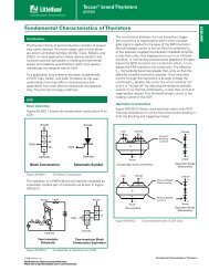
M AN865<br />
Author: Bonnie C. Baker<br />
<strong>Microchip</strong> Technology Inc.<br />
INTRODUCTION<br />
Photo sensors bridge the gap between light and electronics.<br />
<strong>Microchip</strong>’s <strong>Programmable</strong> <strong>Gain</strong> <strong>Amplifier</strong>s<br />
(PGAs) are not well suited for precision applications<br />
(such as CT scanners), but they can be effectively used<br />
in position photo sensing applications minus the headaches<br />
of amplifier stability. When the two, six or eightchannel<br />
PGA is used in this system, the other channels<br />
can be used for other sensors or an array of photo sensors<br />
<strong>with</strong>out an increase in signal conditioning hardware<br />
or PICmicro ® microcontroller I/O pin consumption. The<br />
multiplexer and high-speed conversion response of the<br />
PGA / Analog-to-Digital (A/D) conversion allows the<br />
photo sensor input signal to be sampled and quickly<br />
0.1 uF<br />
R 1 =<br />
10 to<br />
500 kΩ<br />
(typ)<br />
<strong>Sensing</strong> <strong>Light</strong> <strong>with</strong> a <strong>Programmable</strong> <strong>Gain</strong> <strong>Amplifier</strong><br />
V DD<br />
D 1<br />
UDT<br />
PIN-5D<br />
0.1 uF<br />
V DD<br />
14<br />
2 CH0<br />
+<br />
D2 UDT<br />
PIN-5DP<br />
3<br />
4<br />
5<br />
CH1<br />
CH2<br />
CH3<br />
MUX<br />
Internal<br />
PGA<br />
–<br />
6 CH4<br />
VDD 7 CH5<br />
0.1 uF<br />
VREF MCP6S26<br />
A<br />
MCP41100<br />
8,5<br />
W 6 3<br />
+<br />
VDD 0.1 uF<br />
8<br />
8 9<br />
B<br />
4,7 1 3 2<br />
1<br />
MCP6022<br />
2<br />
0.1 uF –<br />
4<br />
4.15<br />
1 kΩ<br />
13<br />
11<br />
10<br />
converted to the digital domain. Switching from channel-to-channel<br />
is then easier <strong>with</strong> the Serial Peripheral<br />
Interface (SPI) from the PICmicro microcontroller to<br />
the PGA.<br />
The PGA can be configured <strong>with</strong> a photo sensor in two<br />
different settings, as illustrated in Figure 1. These circuits<br />
are appropriate for signal responses from DC to<br />
~100 kHz.<br />
For digital sensing, the low pass<br />
filter and ADC can be bypassed.<br />
6.8 nF<br />
VDD VDD<br />
0.1 uF 0.1 uF<br />
2.2 nF<br />
6<br />
1 8<br />
5<br />
2<br />
6<br />
MCP3201<br />
7<br />
3<br />
4<br />
CS_ADC<br />
SDI<br />
/SDO<br />
SCK<br />
CS_PGA<br />
CS_POT<br />
FIGURE 1: Photo sensors can be connected directly to <strong>Microchip</strong>’s PGA. Based on the level of<br />
luminance to the photo sensor, the gain of the signal can be changed through the SPI port of the<br />
MCP6S26, six-channel PGA.<br />
© 2003 <strong>Microchip</strong> Technology Inc. DS00865A-page 1<br />
16.3<br />
kΩ<br />
5<br />
+<br />
MCP6022<br />
–<br />
7<br />
SDO<br />
Digital<br />
In<br />
PIC16C63
AN865<br />
THE PHOTO SENSORS, VOLTAGE<br />
REFERENCE AND PGA<br />
The photo sensor connected to CH0 of the MCP6S26<br />
in Figure 1 uses the photo sensor diode (D1 ) in its photoconductive<br />
mode. When a diode is configured in its<br />
photoconductive mode, it has a reverse voltage bias<br />
applied. In this mode, the photo sensor is optimized for<br />
fast response to light sources. An ideal application for<br />
a diode configured in the photoconductive mode is digital<br />
communications. The reverse biasing of D1 will create<br />
some current leakage and a voltage drop across<br />
the resistor (R1 ). If the offset caused by this leakage<br />
current is not tolerable, it can be calibrated by adjusting<br />
the value of R1. In this scenario, pin 8 (VREF) of the<br />
PGA would be grounded.<br />
The voltage generated by the photo sensor is gained<br />
by the PGA. Consequently, in this configuration, the<br />
PGA would be programmed to higher gains and the<br />
value of the resistor R1, should be selected as low as<br />
possible. This resistor selection is dependant on the<br />
characteristics of the photo sensor. A reasonable range<br />
for R1 would be 10 kΩ to 500 kΩ.<br />
The photo sensor D2, connected to CH1 in Figure 1, is<br />
configured in its photovoltaic mode. For a photo sensor<br />
to be configured in this mode, it must be zero biased.<br />
The configuration shown in Figure 1 is not ideal in this<br />
mode because the voltage across the photo sensor is<br />
not forced to zero by the amplifier. However, the photo<br />
sensor gives an output voltage response near ground<br />
for no light and will increase <strong>with</strong> changes in light. The<br />
PGA gain for this circuit is dependent on the changes<br />
in luminance in the system and the specific photo sensor.<br />
Higher gains will give you a better dynamic range<br />
on the output of the PGA.<br />
PGA Reference Voltage for Linear<br />
Operation<br />
The voltage reference to the PGA can be set using a<br />
voltage reference device. A variable voltage reference<br />
may be required because of the various requirements<br />
on other channels of the PGA. If a variable voltage<br />
reference is needed, the circuit in Figure 1 can be<br />
used.<br />
The input range of the reference voltage pin of the PGA<br />
is VSS to VDD. In this case, VSS = Ground and VDD =<br />
5V. The transfer function of the PGA is equal to:<br />
EQUATION<br />
VOUT = GVIN– ( G – 1)VREF<br />
With this ideal formula, the actual restrictions of the output<br />
of the PGA should be taken into consideration.<br />
Generally speaking, the output swing of the PGA is less<br />
than 20 mV below the positive rail and 125 mV above<br />
ground, as specified in the MCP6S2X PGA data sheet<br />
(DS21117). However, to obtain good, linear performance,<br />
the output should be kept <strong>with</strong>in 300 mV from<br />
the rails. This is specified in the conditions of the “DC<br />
gain error” and “DC output non-linearity” in the<br />
MCP6S2X product data sheet.<br />
Consequently, beyond the absolute voltage limitations<br />
on the PGA voltage reference pin, the voltage output<br />
swing capability further limits the selection of the<br />
voltage at pin 8. This is illustrated in Figure 2 and<br />
Figure 3.<br />
Photo sensors can be connected directly to the PGA<br />
<strong>with</strong> reasonable accuracy. Based on the level of luminance<br />
to the photo sensor, the gain of the signal can be<br />
changed through the SPI port of the MCP6S26, sixchannel<br />
PGA.<br />
1.0<br />
Input Voltage must be lower<br />
0.5<br />
0.0<br />
to insure near zero output<br />
swing from the PGA<br />
0.0 0.5 1.0 1.5 2.0 2.5 3.0 3.5 4.0 4.5 5.0<br />
PGA Reference Voltage (V)<br />
FIGURE 2: If the programmed gain of<br />
the PGA is 2 V/V, the suggested voltage applied<br />
to the V REF (pin 8) is shown in this graph in order<br />
to keep the PGA in its linear region (solid lines)<br />
and to achieve good digital output states (dashed<br />
lines) from the PGA.<br />
FIGURE 3: If the programmed gain of<br />
the PGA is 32, the suggested voltage applied to<br />
the V REF (pin 8) is shown in this graph in order to<br />
keep the PGA in its linear region.<br />
As shown in Figure 2 and Figure 3, the reference voltage<br />
of the PGA should be programmed between the<br />
expected input voltage range of the PGA. For instance,<br />
in a gain of 2 V/V (Figure 2, solid lines), <strong>with</strong> an input<br />
DS00865A-page 2 © 2003 <strong>Microchip</strong> Technology Inc.<br />
PGA Min. and Max. Input Range (V)<br />
Min and Max Input Voltage (V)<br />
5.0<br />
4.5<br />
4.0<br />
3.5<br />
3.0<br />
2.5<br />
2.0<br />
1.5<br />
PGA G = 2V/V Input voltage must be<br />
VDD = 5V higher to insure full scale<br />
output swing from the PGA<br />
Linear Input Voltage<br />
Range of PGA<br />
PGA Output Min = 0.3V<br />
PGA Output Max = 4.7V<br />
5.0<br />
4.5<br />
PGA G = 32V/V<br />
PGA Output Min = 0V<br />
Maximum Input Voltage<br />
to the PGA<br />
4.0 PGA Output Max = 5V<br />
3.5<br />
VDD = 5V<br />
3.0<br />
Minimum Input Voltage<br />
2.5<br />
2.0<br />
1.5<br />
1.0<br />
0.5<br />
0.0<br />
to the PGA<br />
0.0 0.5 1.0 1.5 2.0 2.5 3.0 3.5 4.0 4.5 5.0<br />
PGA Reference Voltage (V)
ange of 1.0V to 3.2V, the voltage reference at pin 8 of<br />
the MCP6S26 should be equal to 1.7V for optimum<br />
performance.<br />
The formulas used to calculate the limits in Figure 2<br />
and Figure 3 are<br />
EQUATION<br />
VIN( min)<br />
≥ ( VOUT( min)<br />
+ ( G – 1)VREF)<br />
⁄ G<br />
VIN( max)<br />
≥ ( VOUT( max)<br />
+ ( G – 1)VREF)<br />
⁄ G<br />
where:<br />
VIN = input voltage to the PGA.<br />
VOUT (min) = minimum output voltage of PGA<br />
= VSS + 0.3V.<br />
VOUT(max) = minimum output voltage of PGA<br />
= VDD - 0.3V.<br />
G = gain of the PGA.<br />
VREF = Voltage applied to the PGA’s VREF pin.<br />
PGA Reference Voltage for Digital<br />
Operation<br />
The reference to the PGA in Figure 1 (MCP6S26, pin 8)<br />
is provided by the digital potentiometer, MCP41100.<br />
Alternatively, the voltage reference pin of the PGA can<br />
be driven <strong>with</strong> a D/A voltage-out converter, a dedicated<br />
voltage reference chip, a resistive divider circuit or tied<br />
to ground or VDD. In all cases, the voltage reference<br />
source should be low-impedance. A digitally-controlled<br />
variable voltage reference may be required because of<br />
the various requirements on other channels of the<br />
PGA. If a variable voltage reference is required, the<br />
circuit in Figure 1 can be used.<br />
As stated in the previous section, the input range of the<br />
reference voltage pin is VSS to VDD, <strong>with</strong> the transfer<br />
function of the PGA equal to:<br />
EQUATION<br />
VOUT =<br />
GVIN– ( G – 1)VREF<br />
To keep the PGA close to the output rail, the PGA output<br />
limits described in the previous section have been<br />
changed to VOUT(min) = 0V as a minimum and<br />
VOUT(max) = 5V as a maximum (although the outputs<br />
will only go to ~20 mV from ground and ~125 mV below<br />
the positive rail).<br />
This concept is illustrated in Figure 2 (dashed lines)<br />
<strong>with</strong> a programmed gain of 2 V/V. This concept is not<br />
illustrated in Figure 3 <strong>with</strong> a programmed gain of<br />
32 V/V because it is difficult to graphically see the difference<br />
between the linear region of operation and the<br />
digital region of operation.<br />
AN865<br />
HANDLING THE OUTPUT OF THE<br />
PGA<br />
In Figure 1, the output of the PGA is shown as having<br />
two possible paths. The solid lines of this circuit follow<br />
the analog path that has a low pass, anti-aliasing filter,<br />
followed by an ADC and then into the a PICmicro<br />
microcontroller. The second path is indicated <strong>with</strong> the<br />
dash lines above the filter and ADC. This is a purely<br />
digital path where the PGA circuit should be designed<br />
to operate as a comparator instead of an analog<br />
component.<br />
Getting a Linear Response<br />
To get a linear response from the photo sensor, the signal<br />
path takes the photo sensor signal from the output<br />
of the PGA, through an anti-aliasing filter, into an ADC<br />
and then to the PICmicro microcontroller for further<br />
processing.<br />
For this function, the PGA should be calibrated to be in<br />
a linear mode. This calibration can be done graphically<br />
as described above or <strong>with</strong> an iterative process. The<br />
first step is to calibrate the maximum luminance on the<br />
photo sensor. The output of the PGA should be at least<br />
300 mV below the power supply (VDD). This is done by<br />
adjusting the gain of the PGA. Once this is achieved,<br />
the minimum luminance should be calibrated. This is<br />
accomplished by exposing the photo sensor to the minimum<br />
luminance condition and adjusting the voltage at<br />
the VREF pin so that the output of the PGA is above<br />
300 mV from VSS. Once this is complete, you should<br />
return to the maximum luminance condition to verify<br />
that the output of PGA is still in its linear region, more<br />
than 300 mV below VDD .<br />
At the output of the PGA, an anti-aliasing filter is<br />
inserted. This is done prior to the A/D conversion in<br />
order to reduce noise. The anti-aliasing filter can be<br />
designed <strong>with</strong> a gain of one or higher, depending on the<br />
circuit requirements. Again, the MCP6022 operational<br />
amplifier is used to match the frequency response of<br />
the PGA. <strong>Microchip</strong>’s FilterLAB ® software can be used<br />
to easily design this filter’s frequency cut-off and gain.<br />
The anti-aliasing filter in this circuit is a Sallen-Key<br />
(non-inverting configuration) <strong>with</strong> a cut-off frequency of<br />
5 kHz. This frequency should be selected to match the<br />
frequency response of interest from the photo sensor,<br />
as well as the other channels at the input of the PGA.<br />
For more information concerning the design of antialiasing<br />
filters, refer to <strong>Microchip</strong> Technology’s AN699,<br />
“Anti-Aliasing, Analog Filters for Data Acquisition<br />
Systems” (DS00699).<br />
The signal at the output of the filter is then connected<br />
to the input of a 12-bit ADC, MCP3201. In this circuit, if<br />
noise is kept under control, it is possible to obtain 12bit<br />
accuracy from the converter. Noise is kept under<br />
control by using an anti-aliasing filter (as shown in<br />
Figure 1), appropriate bypass capacitors, short traces,<br />
© 2003 <strong>Microchip</strong> Technology Inc. DS00865A-page 3
AN865<br />
linear supplies and a solid ground plane. The entire<br />
system is manipulated on the same SPI bus of the<br />
PIC16C63 for the PGA, digital potentiometer and ADC<br />
<strong>with</strong> no digital feed-through from the converter during<br />
conversion.<br />
Opting for the Digital Response<br />
This signal path in Figure 1 is indicated by a dashed<br />
line coming out of the PGA and proceeding directly to<br />
the PICmicro microcontroller. Since the levels of this<br />
line should be high and low, the PGA should be configured<br />
to produce signals near the power supply rails.<br />
The calibration of this system can be performed as discussed<br />
above or by using an iterative method, as<br />
described below.<br />
The first step to iterative calibration is to calibrate the<br />
maximum luminance on the photo sensor. The output<br />
of the PGA should be several millivolts below the power<br />
supply (VDD). This is accomplished by adjusting the<br />
gain of the PGA. In this condition, the output of the PGA<br />
is pushed to exceed the power supply voltage <strong>with</strong> little<br />
effect. If the PGA gain is set too high, the device will go<br />
into a deep saturation. This will slow down the recovery<br />
time of the PGA from high to low.<br />
Once the maximum luminance is properly adjusted, the<br />
minimum luminance should be calibrated. This is done<br />
by exposing the photo sensor to the minimum luminance<br />
condition and adjusting the voltage at VREF so<br />
that the output of the PGA is a few tens of millivolts<br />
above VSS . Once this is complete, you should return to<br />
the maximum luminance condition to verify that the output<br />
of PGA is still close enough to VDD .<br />
Performance Data<br />
This data was taken using an MCP6S26 and one of<br />
each of the photo sensors from UDT sensors. The<br />
selected photo sensors for this application note are not<br />
necessarily the appropriate diodes for all applications.<br />
V DD was equal to 5V and V SS equal to ground. The<br />
data is reported reliably, but does not represent a statistical<br />
sample of the performance of all devices in the<br />
product family.<br />
LINEAR RESPONSE<br />
The photo sensor used in this application note for D2 is<br />
a PIN-5DP/SB from UDT sensors. The size of the<br />
photo sensor is 5.1 mil 2 , <strong>with</strong> a rated capacitance<br />
across the diode at zero bias of 450 pF (typ). This<br />
photo sensor is a Super Blue Enhanced diode from<br />
UDT sensors <strong>with</strong> a responsivity 0.6 A/W at 970 nm.<br />
The shunt resistance at zero bias is 150 MΩ (typ). This<br />
photo sensor is suitable for sensing low level light.<br />
The PIN-5DP/SB was biased in its photovoltaic mode,<br />
as illustrated in Figure 1. When the photo sensor was<br />
placed in a dark environment, the output voltage of the<br />
PGA was 1.8 mV. This output voltage was above VSS and was limited by the output swing of the PGA.<br />
When this set-up was exposed to the lab lighting, the<br />
luminance dictated maximum PGA gain of 10 V/V. This<br />
gain was found through experimentation. The circuit<br />
response under full exposure is shown in Figure 4 and<br />
Figure 5.<br />
FIGURE 4: Using the circuit in Figure 1,<br />
the output code from the 12-bit ADC is collected<br />
while the lab is fully lit.<br />
In Figure 4, the average center code is 2582, which<br />
translates to a voltage is 3.15V <strong>with</strong> a 5V reference on<br />
the ADC. There is a small signal riding on this output<br />
response. This small signal is magnified and shown in<br />
Figure 5. The small signal frequency measured was<br />
120.9 Hz, the ac frequency from the lab lights.<br />
FIGURE 5: The data taken in Figure 4<br />
has been amplified to view the small signal.<br />
DS00865A-page 4 © 2003 <strong>Microchip</strong> Technology Inc.<br />
Output Code<br />
Output Code<br />
4000<br />
3000<br />
2000<br />
1000<br />
2590<br />
2580<br />
2570<br />
Sample Speed = 40 ksps Samples = 1024 Sample Time = 25.6 msec<br />
100 200 300 400 500<br />
Points<br />
600 700 800 900 1000<br />
Sample Speed = 40 kspsSamples = 1024 Sample Time = 25.6 msec.<br />
100 200 300 400 500<br />
Points<br />
600 700 800 900 1000
DIGITAL RESPONSE<br />
The photo sensor used for D1 is a UDT, PIN-5D. It’s silicon<br />
size is the same as D2 at 5.1mil 2 , however, its<br />
responsivity at 410 nm is 0.2 A/W. This photo sensor is<br />
specifically manufactured for digital, high-speed<br />
response, having a parasitic capacitance across the<br />
element of 15 pF <strong>with</strong> a -10V reverse bias.<br />
The Dark Current leakage of this photo sensor <strong>with</strong> a<br />
reverse bias of -10V is specified as 3 nA (max). This<br />
specification was used to calculate an appropriate<br />
value for R1 .<br />
EQUATION<br />
G • VOUT( min)<br />
R1 ≤ --------------------------------------<br />
IDC( max)<br />
1V/V • 1V<br />
R1 ≤ -----------------------<br />
3 nA<br />
R1 ≤<br />
333 mΩ<br />
where:<br />
VOUT (min) = VIL of a Schmitt Trigger buffer<br />
input pin of the PIC16C63 and<br />
IDC(max) = the maximum Dark Current leakage<br />
of the photo sensor<br />
R 1 was chosen to be 10 kΩ for noise reduction purposes.<br />
In this test, the MCP6S26 was programmed to<br />
a gain of 1 V/V. The output swings from 100 mV to<br />
4.95V, dependent on the level of light exposure.<br />
CONCLUSION<br />
AN865<br />
Position sensing <strong>with</strong> the MCP6S2X PGA devices from<br />
<strong>Microchip</strong> Technology Inc. is easily implemented. The<br />
connections described in this application note can easily<br />
be implemented in a sensing system that has several<br />
channels for other functions. The MCP6S2X family<br />
of PGAs have one, two, six or eight-channel devices in<br />
the product offering. Changing from channel to channel<br />
may entail a gain and reference voltage change. This<br />
would require that three, 16-bit communications occur<br />
between the PGA and digital potentiometer. With a<br />
clock rate of 10 MHz on the SPI interface, this would<br />
require approximately 3.4 ms; 1.7 ms per device. Additionally,<br />
the PGA amplifier would need to settle. Refer<br />
to the MCP6S2X PGA data sheet (DS21117) for the<br />
settling time versus gain specification.<br />
The PGA, a device from <strong>Microchip</strong> Technology Inc., not<br />
only offers excellent offset voltage performance, but<br />
the configurations in these optical sensing circuits are<br />
easily designed <strong>with</strong>out the headaches of stability that<br />
the stand-alone amplifier circuits present to the<br />
designer. Stability <strong>with</strong> these programmable gain<br />
amplifiers have been built-in by <strong>Microchip</strong> engineers.<br />
References<br />
AN699, “Anti-Aliasing, Analog Filters for Data Acquisition<br />
Systems”, Bonnie C. Baker, <strong>Microchip</strong> Technology<br />
Inc. (DS00699).<br />
© 2003 <strong>Microchip</strong> Technology Inc. DS00865A-page 5
AN865<br />
NOTES:<br />
DS00865A-page 6 © 2003 <strong>Microchip</strong> Technology Inc.
Note the following details of the code protection feature on <strong>Microchip</strong> devices:<br />
• <strong>Microchip</strong> products meet the specification contained in their particular <strong>Microchip</strong> Data Sheet.<br />
• <strong>Microchip</strong> believes that its family of products is one of the most secure families of its kind on the market today, when used in the<br />
intended manner and under normal conditions.<br />
• There are dishonest and possibly illegal methods used to breach the code protection feature. All of these methods, to our<br />
knowledge, require using the <strong>Microchip</strong> products in a manner outside the operating specifications contained in <strong>Microchip</strong>'s Data<br />
Sheets. Most likely, the person doing so is engaged in theft of intellectual property.<br />
• <strong>Microchip</strong> is willing to work <strong>with</strong> the customer who is concerned about the integrity of their code.<br />
• Neither <strong>Microchip</strong> nor any other semiconductor manufacturer can guarantee the security of their code. Code protection does not<br />
mean that we are guaranteeing the product as “unbreakable.”<br />
Code protection is constantly evolving. We at <strong>Microchip</strong> are committed to continuously improving the code protection features of our<br />
products. Attempts to break microchip’s code protection feature may be a violation of the Digital Millennium Copyright Act. If such<br />
acts allow unauthorized access to your software or other copyrighted work, you may have a right to sue for relief under that Act.<br />
Information contained in this publication regarding device<br />
applications and the like is intended through suggestion only<br />
and may be superseded by updates. It is your responsibility to<br />
ensure that your application meets <strong>with</strong> your specifications. No<br />
representation or warranty is given and no liability is assumed<br />
by <strong>Microchip</strong> Technology Incorporated <strong>with</strong> respect to the<br />
accuracy or use of such information, or infringement of patents<br />
or other intellectual property rights arising from such use or<br />
otherwise. Use of <strong>Microchip</strong>’s products as critical components in<br />
life support systems is not authorized except <strong>with</strong> express<br />
written approval by <strong>Microchip</strong>. No licenses are conveyed,<br />
implicitly or otherwise, under any intellectual property rights.<br />
Trademarks<br />
The <strong>Microchip</strong> name and logo, the <strong>Microchip</strong> logo, KEELOQ,<br />
MPLAB, PIC, PICmicro, PICSTART, PRO MATE and<br />
PowerSmart are registered trademarks of <strong>Microchip</strong> Technology<br />
Incorporated in the U.S.A. and other countries.<br />
FilterLab, microID, MXDEV, MXLAB, PICMASTER, SEEVAL<br />
and The Embedded Control Solutions Company are registered<br />
trademarks of <strong>Microchip</strong> Technology Incorporated in the U.S.A.<br />
Accuron, Application Maestro, dsPIC, dsPICDEM,<br />
dsPICDEM.net, ECONOMONITOR, FanSense, FlexROM,<br />
fuzzyLAB, In-Circuit Serial Programming, ICSP, ICEPIC,<br />
microPort, Migratable Memory, MPASM, MPLIB, MPLINK,<br />
MPSIM, PICC, PICkit, PICDEM, PICDEM.net, PowerCal,<br />
PowerInfo, PowerMate, PowerTool, rfLAB, rfPIC, Select Mode,<br />
SmartSensor, SmartShunt, SmartTel and Total Endurance are<br />
trademarks of <strong>Microchip</strong> Technology Incorporated in the U.S.A.<br />
and other countries.<br />
Serialized Quick Turn Programming (SQTP) is a service mark of<br />
<strong>Microchip</strong> Technology Incorporated in the U.S.A.<br />
All other trademarks mentioned herein are property of their<br />
respective companies.<br />
© 2003, <strong>Microchip</strong> Technology Incorporated, Printed in the<br />
U.S.A., All Rights Reserved.<br />
Printed on recycled paper.<br />
<strong>Microchip</strong> received QS-9000 quality system<br />
certification for its worldwide headquarters,<br />
design and wafer fabrication facilities in<br />
Chandler and Tempe, Arizona in July 1999<br />
and Mountain View, California in March 2002.<br />
The Company’s quality system processes and<br />
procedures are QS-9000 compliant for its<br />
PICmicro ® 8-bit MCUs, KEELOQ ® code hopping<br />
devices, Serial EEPROMs, microperipherals,<br />
non-volatile memory and analog products. In<br />
addition, <strong>Microchip</strong>’s quality system for the<br />
design and manufacture of development<br />
systems is ISO 9001 certified.<br />
© 2003 <strong>Microchip</strong> Technology Inc. Preliminary DS00865A - page 7
M<br />
AMERICAS<br />
Corporate Office<br />
2355 West Chandler Blvd.<br />
Chandler, AZ 85224-6199<br />
Tel: 480-792-7200 Fax: 480-792-7277<br />
Technical Support: 480-792-7627<br />
Web Address: http://www.microchip.com<br />
Atlanta<br />
3780 Mansell Road, Suite 130<br />
Alpharetta, GA 30022<br />
Tel: 770-640-0034 Fax: 770-640-0307<br />
Boston<br />
2 Lan Drive, Suite 120<br />
Westford, MA 01886<br />
Tel: 978-692-3848 Fax: 978-692-3821<br />
Chicago<br />
333 Pierce Road, Suite 180<br />
Itasca, IL 60143<br />
Tel: 630-285-0071 Fax: 630-285-0075<br />
Dallas<br />
4570 Westgrove Drive, Suite 160<br />
Addison, TX 75001<br />
Tel: 972-818-7423 Fax: 972-818-2924<br />
Detroit<br />
Tri-Atria Office Building<br />
32255 Northwestern Highway, Suite 190<br />
Farmington Hills, MI 48334<br />
Tel: 248-538-2250 Fax: 248-538-2260<br />
Kokomo<br />
2767 S. Albright Road<br />
Kokomo, Indiana 46902<br />
Tel: 765-864-8360 Fax: 765-864-8387<br />
Los Angeles<br />
18201 Von Karman, Suite 1090<br />
Irvine, CA 92612<br />
Tel: 949-263-1888 Fax: 949-263-1338<br />
Phoenix<br />
2355 West Chandler Blvd.<br />
Chandler, AZ 85224-6199<br />
Tel: 480-792-7966 Fax: 480-792-4338<br />
San Jose<br />
<strong>Microchip</strong> Technology Inc.<br />
2107 North First Street, Suite 590<br />
San Jose, CA 95131<br />
Tel: 408-436-7950 Fax: 408-436-7955<br />
Toronto<br />
6285 Northam Drive, Suite 108<br />
Mississauga, Ontario L4V 1X5, Canada<br />
Tel: 905-673-0699 Fax: 905-673-6509<br />
WORLDWIDE SALES AND SERVICE<br />
ASIA/PACIFIC<br />
Australia<br />
<strong>Microchip</strong> Technology Australia Pty Ltd<br />
Marketing Support Division<br />
Suite 22, 41 Rawson Street<br />
Epping 2121, NSW<br />
Australia<br />
Tel: 61-2-9868-6733 Fax: 61-2-9868-6755<br />
China - Beijing<br />
<strong>Microchip</strong> Technology Consulting (Shanghai)<br />
Co., Ltd., Beijing Liaison Office<br />
Unit 915<br />
Bei Hai Wan Tai Bldg.<br />
No. 6 Chaoyangmen Beidajie<br />
Beijing, 100027, No. China<br />
Tel: 86-10-85282100 Fax: 86-10-85282104<br />
China - Chengdu<br />
<strong>Microchip</strong> Technology Consulting (Shanghai)<br />
Co., Ltd., Chengdu Liaison Office<br />
Rm. 2401-2402, 24th Floor,<br />
Ming Xing Financial Tower<br />
No. 88 TIDU Street<br />
Chengdu 610016, China<br />
Tel: 86-28-86766200 Fax: 86-28-86766599<br />
China - Fuzhou<br />
<strong>Microchip</strong> Technology Consulting (Shanghai)<br />
Co., Ltd., Fuzhou Liaison Office<br />
Unit 28F, World Trade Plaza<br />
No. 71 Wusi Road<br />
Fuzhou 350001, China<br />
Tel: 86-591-7503506 Fax: 86-591-7503521<br />
China - Hong Kong SAR<br />
<strong>Microchip</strong> Technology Hongkong Ltd.<br />
Unit 901-6, Tower 2, Metroplaza<br />
223 Hing Fong Road<br />
Kwai Fong, N.T., Hong Kong<br />
Tel: 852-2401-1200 Fax: 852-2401-3431<br />
China - Shanghai<br />
<strong>Microchip</strong> Technology Consulting (Shanghai)<br />
Co., Ltd.<br />
Room 701, Bldg. B<br />
Far East International Plaza<br />
No. 317 Xian Xia Road<br />
Shanghai, 200051<br />
Tel: 86-21-6275-5700 Fax: 86-21-6275-5060<br />
China - Shenzhen<br />
<strong>Microchip</strong> Technology Consulting (Shanghai)<br />
Co., Ltd., Shenzhen Liaison Office<br />
Rm. 1812, 18/F, Building A, United Plaza<br />
No. 5022 Binhe Road, Futian District<br />
Shenzhen 518033, China<br />
Tel: 86-755-82901380 Fax: 86-755-82966626<br />
China - Qingdao<br />
Rm. B505A, Fullhope Plaza,<br />
No. 12 Hong Kong Central Rd.<br />
Qingdao 266071, China<br />
Tel: 86-532-5027355 Fax: 86-532-5027205<br />
India<br />
<strong>Microchip</strong> Technology Inc.<br />
India Liaison Office<br />
Marketing Support Division<br />
Divyasree Chambers<br />
1 Floor, Wing A (A3/A4)<br />
No. 11, O’Shaugnessey Road<br />
Bangalore, 560 025, India<br />
Tel: 91-80-2290061 Fax: 91-80-2290062<br />
Japan<br />
<strong>Microchip</strong> Technology Japan K.K.<br />
Benex S-1 6F<br />
3-18-20, Shinyokohama<br />
Kohoku-Ku, Yokohama-shi<br />
Kanagawa, 222-0033, Japan<br />
Tel: 81-45-471- 6166 Fax: 81-45-471-6122<br />
Korea<br />
<strong>Microchip</strong> Technology Korea<br />
168-1, Youngbo Bldg. 3 Floor<br />
Samsung-Dong, Kangnam-Ku<br />
Seoul, Korea 135-882<br />
Tel: 82-2-554-7200 Fax: 82-2-558-5934<br />
Singapore<br />
<strong>Microchip</strong> Technology Singapore Pte Ltd.<br />
200 Middle Road<br />
#07-02 Prime Centre<br />
Singapore, 188980<br />
Tel: 65-6334-8870 Fax: 65-6334-8850<br />
Taiwan<br />
<strong>Microchip</strong> Technology (Barbados) Inc.,<br />
Taiwan Branch<br />
11F-3, No. 207<br />
Tung Hua North Road<br />
Taipei, 105, Taiwan<br />
Tel: 886-2-2717-7175 Fax: 886-2-2545-0139<br />
EUROPE<br />
Austria<br />
<strong>Microchip</strong> Technology Austria GmbH<br />
Durisolstrasse 2<br />
A-4600 Wels<br />
Austria<br />
Tel: 43-7242-2244-399<br />
Fax: 43-7242-2244-393<br />
Denmark<br />
<strong>Microchip</strong> Technology Nordic ApS<br />
Regus Business Centre<br />
Lautrup hoj 1-3<br />
Ballerup DK-2750 Denmark<br />
Tel: 45 4420 9895 Fax: 45 4420 9910<br />
France<br />
<strong>Microchip</strong> Technology SARL<br />
Parc d’Activite du Moulin de Massy<br />
43 Rue du Saule Trapu<br />
Batiment A - ler Etage<br />
91300 Massy, France<br />
Tel: 33-1-69-53-63-20 Fax: 33-1-69-30-90-79<br />
Germany<br />
<strong>Microchip</strong> Technology GmbH<br />
Steinheilstrasse 10<br />
D-85737 Ismaning, Germany<br />
Tel: 49-89-627-144-0<br />
Fax: 49-89-627-144-44<br />
Italy<br />
<strong>Microchip</strong> Technology SRL<br />
Via Quasimodo, 12<br />
20025 Legnano (MI)<br />
Milan, Italy<br />
Tel: 39-0331-742611 Fax: 39-0331-466781<br />
United Kingdom<br />
<strong>Microchip</strong> Ltd.<br />
505 Eskdale Road<br />
Winnersh Triangle<br />
Wokingham<br />
Berkshire, England RG41 5TU<br />
Tel: 44 118 921 5869 Fax: 44-118 921-5820<br />
DS00865A-page 8 © 2003 <strong>Microchip</strong> Technology Inc.<br />
03/25/03