AN-1055 Low-Cost Multiple Output Flyback Converter for ... - Bitsavers
AN-1055 Low-Cost Multiple Output Flyback Converter for ... - Bitsavers
AN-1055 Low-Cost Multiple Output Flyback Converter for ... - Bitsavers

You also want an ePaper? Increase the reach of your titles
YUMPU automatically turns print PDFs into web optimized ePapers that Google loves.
<strong>Low</strong>-<strong>Cost</strong> <strong>Multiple</strong> <strong>Output</strong><br />
<strong>Flyback</strong> <strong>Converter</strong> <strong>for</strong> IO<br />
Cards<br />
INTRODUCTION<br />
Isolated power supplies <strong>for</strong> IO cards are required to provide<br />
multiple outputs (typically 9V at 0 mA–120 mA and 5V<br />
at 0 mA–200 mA) from a 33V input The trans<strong>for</strong>mer peak<br />
primary currents are generally very high there by eliminating<br />
the choice of many popular low-cost integrated circuits The<br />
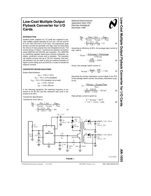
circuits shown in Figure 1 per<strong>for</strong>ms the required conversion<br />
using LM3578A and D44C3A npn transistor The LM3578A<br />
is a switching regulator featuring an internal comparator oscillator<br />
protection circuitry and a transistor The transistor<br />
can handle currents only up to 750 mA However this internal<br />
transistor can be used to drive an external transistor of<br />
higher current rating such as D44C3A in order to handle the<br />
required currents<br />
CONVERTER DESIGN EQUATIONS<br />
System Specifications<br />
VIN e 33V (g10%)<br />
Vo1 e 9V (g10%) (Isolated)<br />
Vo2 e 5V (g5%) (Isolation not a must)<br />
Io1 e 0 mA–120 mA<br />
Io2 e 0 mA–200 mA<br />
In the following equations the switching frequency is assumed<br />
to be 80 kHz and the maximum duty cycle is assumed<br />
to be 50%<br />
Trans<strong>for</strong>mer Specification<br />
Trans<strong>for</strong>mer turns ratio is<br />
Ns1 (Vo1 e<br />
Np<br />
a Vd )<br />
VIN (min) b Vce<br />
Dmax<br />
(sat) 1 b Dmax<br />
(9 a 07 ) 05<br />
e e 36 (1)<br />
(3 b 03 ) 1 b 05<br />
FIGURE 1<br />
National Semiconductor<br />
Application Note <strong>1055</strong><br />
Ravindra Ambatipudi<br />
November 1996<br />
Ns2 (Vo2 e<br />
Np<br />
a Vd )<br />
VIN (min) b Vce<br />
Dmax<br />
(sat) 1 b Dmax<br />
(5 a 07 ) 05<br />
e e 21 (2)<br />
(3 b 03) 1 b 05<br />
Assuming an efficiency of 80% the average input current at<br />
max load is<br />
IIN (dc) e Vo1Io1 (max) a Vo2 Io2 (max)<br />
h VIN (min)<br />
e 208<br />
e 087A (3)<br />
08 (3)<br />
Hence the average switch current is<br />
Isw (avg) e IIN (dc)<br />
D<br />
087<br />
e e 174A (4)<br />
05<br />
Assuming the primary inductance current ripple to be 25%<br />
of the average switch current the primary inductance is given<br />
by<br />
Lp e (VIN (min) b Vce (sat) )Dmax<br />
Dip fs (3 b 03) 05<br />
e e 195 mH (5)<br />
80000 c 1742<br />
Peak primary current is given by<br />
Ip e Isw (avg) a Dip2<br />
e 174 a 1744 e 22A<br />
C1996 National Semiconductor Corporation TLH12878<br />
RRD-B30M17Printed in U S A httpwwwnationalcom<br />
(6)<br />
TLH12878–1<br />
<strong>Low</strong>-<strong>Cost</strong> <strong>Multiple</strong> <strong>Output</strong> <strong>Flyback</strong> <strong>Converter</strong> <strong>for</strong> IO Cards <strong>AN</strong>-<strong>1055</strong>
Transistor Selection<br />
The transistor should be able to handle the peak current<br />
calculated above The internal transistor in LM3578 can<br />
handle up to 750 mA So the current gain of the external<br />
transistor should be greater than 30 at the peak primary<br />
current The off state voltage rating of the switch should be<br />
at least 10V One npn transistor meeting these requirements<br />
is D44C3A<br />
Current Limiting with LM3578A<br />
Current limiting is activated whenever pin 7 is pulled 110 mV<br />
(typically) above the ground In this application voltage<br />
across the resistor Rsn is sensed in order to determine excess<br />
current through the external switch Typical value <strong>for</strong><br />
Rsn is 005X Rsn can also be fabricated on a copper trace<br />
If DT is the estimated temperature rise the resistance of<br />
1 ozft2 copper sheet is given by<br />
Rc(T) e 05c10 (7)<br />
b3 1 a 39c10b3 (TA b 20 a DT)<br />
Where TA is the ambient temperature The required length<br />
(l) and width (w) of copper trace can be calculated using the<br />
following equations<br />
1000 c Ilim<br />
w e (8)<br />
0DT(55 Rc(T))<br />
l e w Rsn Rc(T)<br />
where Ilim is the desired current limit set point<br />
PARTS LIST<br />
(9)<br />
Feedback<br />
Isolation between the 9V output and the input is maintained<br />
by using the 5V output <strong>for</strong> feedback (since the specification<br />
does not require isolation between 5V output and the input)<br />
Thus the need <strong>for</strong> an opto-isolator or other type of feedback-isolation<br />
is eliminated The reference pin (pin 1) is set<br />
at 1V using a resistor divider network (R1R2) Compensation<br />
The switching frequency is set by using the timing capacitor<br />
CT Choosing a value of 1 nF <strong>for</strong> CT sets the switching frequency<br />
at 80 kHz Capacitor C1 (typically between 10 pF–<br />
25 pF) together with the feedback resistors (R1 and R2)is used <strong>for</strong> compensation For more details on choice of the<br />
above components please refer to National Semiconductor<br />
data sheet <strong>for</strong> LM3578A<br />
RESULTS<br />
The output voltage ripple was measured to be equal to 63<br />
mV at the 5V output and 43 mV at the isolated 9V output<br />
Efficiency of this converter was around 78% under nominal<br />
conditions Less than 10% cross-regulation was observed<br />
Designator Quantity ValueRating Description<br />
U1 1 LM3578A Switching Regulator<br />
Q1 1 5A 30V D44C3A NPN Transistor<br />
D1 D2 2 1A 40V <strong>Output</strong> Diodes SR104<br />
D3 1 1A 40V Clamping Diode SR104<br />
ZD1 1 10V Zener diode <strong>for</strong> clamping<br />
T1 1 Lp-242 mH Ip-21A Trans<strong>for</strong>mer<br />
CIN 1 220 mF 63V Input bulk capacitor<br />
C o1 1 470 mF 16V <strong>Output</strong> 1 capacitor<br />
Co2 1 470 mF 10V <strong>Output</strong> 2 capacitor<br />
R sn 1 005X W Current limiting resistor<br />
R1 1 402 kX W Feedback resistor<br />
R2 1 10kXW Feedback resistor<br />
R d1 1 15X W Base drive resistor<br />
Rd2 1 200X W Base drive resistor<br />
R f 1 1kXW Resistor <strong>for</strong> spike suppression<br />
Cf 1 22 nF Capacitor <strong>for</strong> spike suppression<br />
C T 1 1 nF Timing capacitor<br />
Cc 1 1 nF Compensation capacitor<br />
httpwwwnationalcom 2
3<br />
httpwwwnationalcom
<strong>AN</strong>-<strong>1055</strong> <strong>Low</strong>-<strong>Cost</strong> <strong>Multiple</strong> <strong>Output</strong> <strong>Flyback</strong> <strong>Converter</strong> <strong>for</strong> IO Cards<br />
LIFE SUPPORT POLICY<br />
NATIONAL’S PRODUCTS ARE NOT AUTHORIZED FOR USE AS CRITICAL COMPONENTS IN LIFE SUPPORT<br />
DEVICES OR SYSTEMS WITHOUT THE EXPRESS WRITTEN APPROVAL OF THE PRESIDENT OF NATIONAL<br />
SEMICONDUCTOR CORPORATION As used herein<br />
1 Life support devices or systems are devices or 2 A critical component is any component of a life<br />
systems which (a) are intended <strong>for</strong> surgical implant support device or system whose failure to per<strong>for</strong>m can<br />
into the body or (b) support or sustain life and whose be reasonably expected to cause the failure of the life<br />
failure to per<strong>for</strong>m when properly used in accordance support device or system or to affect its safety or<br />
with instructions <strong>for</strong> use provided in the labeling can effectiveness<br />
be reasonably expected to result in a significant injury<br />
to the user<br />
National Semiconductor National Semiconductor National Semiconductor National Semiconductor<br />
Corporation Europe Southeast Asia Japan Ltd<br />
Americas<br />
Fax a49 (0) 180-530 85 86 Fax (852) 2376 3901 Tel 81-3-5620-7561<br />
Tel 1(800) 272-9959<br />
Fax 1(800) 737-7018<br />
Email support nsccom<br />
httpwwwnationalcom<br />
Email europesupport nsccom<br />
Deutsch Tel a49 (0) 180-530 85 85<br />
English Tel a49 (0) 180-532 78 32<br />
Franais Tel a49 (0) 180-532 93 58<br />
Italiano Tel a49 (0) 180-534 16 80<br />
Email seasupport nsccom Fax 81-3-5620-6179<br />
National does not assume any responsibility <strong>for</strong> use of any circuitry described no circuit patent licenses are implied and National reserves the right at any time without notice to change said circuitry and specifications