POWERING your FUTURE
POWERING your FUTURE
POWERING your FUTURE

Create successful ePaper yourself
Turn your PDF publications into a flip-book with our unique Google optimized e-Paper software.
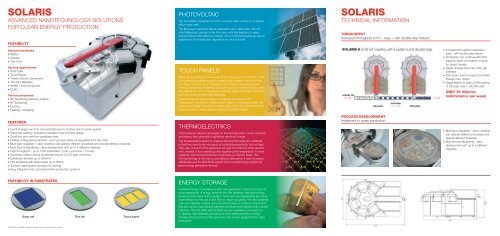
SOLarIS<br />
ADvANCED NANOTECHNOLOGy SOLUTIONS<br />
FOR CLEAN ENERGy PRODUCTION<br />
FLEXIBILITy<br />
Various substrates<br />
Wafers<br />
Glasses<br />
Thin Foils<br />
Various applications<br />
Solar Cells<br />
Touch Panels<br />
Thermo Electric Generators<br />
Thin Film Batteries<br />
NEMS / Semiconductors<br />
OLED<br />
Various processes<br />
DC Sputtering (reactive, pulsed)<br />
RF Sputtering<br />
Etching<br />
Heating / Annealing<br />
FEaTUrES<br />
Quick change over from one substrate size to another due to carrier system<br />
Substrate loading / unloading included in the machine design<br />
Small foot print and low operating costs<br />
Flexible confi gurations allowed - each process station is separated from the other<br />
Multi layer capability – each chamber can operate different processes and deposit different materials<br />
Multi Source Sputtering – alloy development with up to 4 different materials<br />
High throughput – up to 1200 substrates / h (dry cycle time < 3.0 sec)<br />
Substrate rotation during sputtering ensures ±2.5% layer uniformity<br />
Substrate diameter up to 225mm<br />
Film annealing with lamp heater up to 550°C<br />
Surface cleaning and activation by etching<br />
Easy integration into automated inline production systems<br />
FLEXIBILITy IN SUBSTraTES<br />
Solar cell Thin foil Touch panel<br />
SOLARIS is an Oerlikon trademark registered in Europe and other countries<br />
PHOTOvOLTAIC<br />
The SOLARIS is designed for front- and back side coating of crystalline<br />
silicon solar cells.<br />
The Multi layer capability allows passivation and “silane free” SiN-AR<br />
(Anti Refl ective) coating on the front side, with the freedom to select<br />
optical criterias (like refractive indices, etc.) of individual layers as well as<br />
passivation and metal layer deposition on the back side.<br />
TOUCH PANELS<br />
While touch sensing is commonplace for single points of contact, multitouch<br />
sensing enables a user to interact with a system with more than<br />
one fi nger at a time, as in chording and bi-manual operations. Such<br />
sensing devices are inherently also able to accommodate multiple users<br />
simultaneously, which is especially useful for larger interaction scenarios<br />
such as interactive walls and tabletops.<br />
Touch panels are made of glass or polymer and require TCO<br />
(Transparent Conductive Oxide) contact layers in combination with anti<br />
refl ection coatings The ability to mask areas which do not require active<br />
layers is another unique feature with the SOLARIS system.<br />
THERMOELECTRICS<br />
Thermoelectric devices are based on the fact that when certain materials<br />
are heated, they generate a signifi cant electrical voltage.<br />
The fundamental problem in creating effi cient thermoelectric materials<br />
is that they need to be very good at conducting electricity, but not heat.<br />
That way, one end of the apparatus can get hot while the other remains<br />
cold, instead of the material quickly equalizing the temperature. In most<br />
materials, electrical and thermal conductivity go hand in hand. Thin<br />
Film technology is not only a cost effective alternative, it even increases<br />
effi ciencies and the SOLARIS system is the manufacturing solution for<br />
green energy generation devices.<br />
ENERGy STORAGE<br />
Nanotechnology is providing us with next generation systems that rely on<br />
micro-generation of energy stored in thin fi lm batteries. Nanotechnology<br />
works on both sides of the equation. Solar and wind generators are made<br />
more effi cient by the use of thin fi lms to reach grid parity. Thin fi lm batteries<br />
use new materials created using nanotechnology to achieve components<br />
that are used to manufacture batteries 40 times more effi cient than current<br />
batteries. The SOLARIS with its Multi source capability is the ideal tool<br />
to develop new materials and alloys to drive developments in energy<br />
storage devices and is at the same time the proven equipment for mass<br />
production.<br />
SOLarIS<br />
TECHNICAL INFORMATION<br />
THrOUGHpUT<br />
Increased throughput in Pv – easy – with double step feature:<br />
prOCESS DEVELOpmENT<br />
Implement to mass production<br />
Increased throughput necessary –<br />
easy - with double step feature<br />
Production can continue with 50%<br />
capacity when one system is down<br />
for target change<br />
Target change time max. 2min per<br />
chamber<br />
Total down time for target and shield<br />
change max. 30min<br />
Target lifetime in case of SiN coating<br />
of cSi solar cells = 180,000 cells<br />
ONLy 30 minutes<br />
maintenance per week<br />
Multi layer capability – each chamber<br />
can operate different processes and<br />
deposit different materials<br />
Multi Source Sputtering – alloy<br />
development with up to 4 different<br />
materials