datasheet: pdf - Leocom
datasheet: pdf - Leocom
datasheet: pdf - Leocom

Create successful ePaper yourself
Turn your PDF publications into a flip-book with our unique Google optimized e-Paper software.
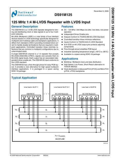
DS91M125<br />
125 MHz 1:4 M-LVDS Repeater with LVDS Input<br />
General Description<br />
The DS91M125 is a 1:4 M-LVDS repeater designed for driving<br />
and distributing clock or data signals to up to four multipoint<br />
networks.<br />
M-LVDS (Multipoint LVDS) is a new family of bus interface<br />
devices based on LVDS technology specifically designed for<br />
multipoint and multidrop cable and backplane applications. It<br />
differs from standard LVDS in providing increased drive current<br />
to handle double terminations that are required in multipoint<br />
applications. Controlled transition times minimize reflections<br />
that are common in multipoint configurations due to<br />
unterminated stubs.<br />
A single DS91M125 channel is a 1:4 repeater that accepts<br />
M-LVDS/LVDS/CML/LVPECL signals and converts them to<br />
M-LVDS signal levels. Each output has an associated independent<br />
driver enable pin. The DS91M125 input conforms to<br />
the LVDS standard.<br />
The DS91M125 has a flow-through pinout for easy PCB layout.<br />
It provides a new alternative for high speed multipoint<br />
interface applications. It is packaged in a space saving<br />
SOIC-16 package.<br />
Typical Application<br />
Features<br />
November 9, 2009<br />
■ DC - 125 MHz / 250 Mbps low jitter, low skew, low power<br />
operation<br />
■ Independent Driver Enable pins<br />
■ Outputs Conform to TIA/EIA-899 M-LVDS Standard<br />
■ Controlled transition times minimize reflections<br />
■ Inputs Conform to TIA/EIA-644-A LVDS Standard<br />
■ 8 kV ESD on M-LVDS output pins protects adjoining<br />
components<br />
■ Flow-through pinout simplifies PCB layout<br />
■ Industrial operating temperature range (−40°C to +85°C)<br />
■ Available in a space saving SOIC-16 package<br />
Applications<br />
■ Multidrop / Multipoint clock and data distribution<br />
■ High-Speed, Low Power, Short-Reach alternative to<br />
TIA/EIA-485/422<br />
■ Clock distribution in AdvancedTCA (ATCA) and MicroTCA<br />
(μTCA, uTCA) backplanes<br />
© 2009 National Semiconductor Corporation 300542 www.national.com<br />
30054202<br />
DS91M125 125 MHz 1:4 M-LVDS Repeater with LVDS Input
DS91M125<br />
Ordering Information<br />
Connection Diagram<br />
Logic Diagram<br />
Pin Descriptions<br />
Order Number Function Package Type<br />
DS91M125TMA 1:4 Repeater SOIC-16<br />
30054201<br />
30054203<br />
Number Name I/O, Type Description<br />
1, 2, 3, 8 DE I, LVCMOS Driver enable pins: When DE is low, the driver is disabled. When<br />
DE is high, the driver is enabled. There is a 300 kΩ pulldown<br />
resistor on each pin.<br />
6 DI+ I, LVDS Non-inverting receiver input pin.<br />
7 DI- I, LVDS Inverting receiver input pin.<br />
5 GND Power Ground pin.<br />
10, 11, 14, 15 A O, M-LVDS Non-inverting driver output pin.<br />
9, 12, 13, 16 B O, M-LVDS Inverting driver output pin.<br />
4 V DD Power Power supply pin, +3.3V ± 0.3V<br />
www.national.com 2
Absolute Maximum Ratings (Note 4)<br />
If Military/Aerospace specified devices are required,<br />
please contact the National Semiconductor Sales Office/<br />
Distributors for availability and specifications.<br />
Supply Voltage −0.3V to +4V<br />
LVCMOS Input Voltages −0.3V to (V DD + 0.3V)<br />
M-LVDS Output Voltages −1.9V to +5.5V<br />
LVDS Input Voltages −0.3V to (V DD + 0.3V)<br />
Maximum Package Power Dissipation at +25°C<br />
SOIC Package 2.21W<br />
Derate SOIC Package 19.2 mW/°C above +25°C<br />
Thermal Resistance (4-Layer, 2 oz. Cu, JEDEC)<br />
θ JA<br />
θ JC<br />
52°C/W<br />
19°C/W<br />
Maximum Junction Temperature 140°C<br />
Storage Temperature Range −65°C to +150°C<br />
Lead Temperature<br />
(Soldering, 4 seconds) 260°C<br />
ESD Susceptibility<br />
HBM (Note 1) ≥ 8 kV<br />
MM (Note 2) ≥ 250V<br />
CDM (Note 3) ≥ 1250V<br />
Note 1: Human Body Model, applicable std. JESD22-A114C<br />
Note 2: Machine Model, applicable std. JESD22-A115-A<br />
Note 3: Field Induced Charge Device Model, applicable std.<br />
JESD22-C101-C<br />
Recommended Operating<br />
Conditions<br />
Min Typ Max Units<br />
Supply Voltage, V DD 3.0 3.3 3.6 V<br />
Voltage at M-LVDS Outputs −1.4 +3.8 V<br />
Voltage at LVDS Inputs 0 V DD V<br />
LVCMOS Input Voltage High V IH 2.0 V DD V<br />
LVCMOS Input Voltage Low V IL 0 0.8 V<br />
Operating Free Air<br />
Temperature T A −40 +25 +85 °C<br />
Electrical Characteristics<br />
Over recommended operating supply and temperature ranges unless otherwise specified. (Note 5, Note 6, Note 7, Note 10)<br />
Symbol Parameter Conditions Min Typ Max Units<br />
LVCMOS DC Specifications<br />
V IH High-Level Input Voltage 2.0 V DD V<br />
V IL Low-Level Input Voltage GND 0.8 V<br />
I IH High-Level Input Current V IH = 3.6V -15 ±1 15 μA<br />
I IL Low-Level Input Current V IL = 0V -15 ±1 15 μA<br />
V CL Input Clamp Voltage I IN = -18 mA -1.5 V<br />
M-LVDS Driver DC Specifications<br />
|V AB | Differential output voltage magnitude R L = 50Ω, C L = 5pF 480 650 mV<br />
ΔV AB<br />
Change in differential output voltage magnitude<br />
between logic states<br />
Figures 1, 3<br />
−50 0 +50 mV<br />
V OS(SS) Steady-state common-mode output voltage R L = 50Ω, C L = 5pF 0.3 1.6 2.1 V<br />
|ΔV OS(SS) | Change in steady-state common-mode output<br />
voltage between logic states<br />
Figures 1, 2<br />
0 +50 mV<br />
V A(OC) Maximum steady-state open-circuit output voltage Figure 4 0 2.4 V<br />
V B(OC) Maximum steady-state open-circuit output voltage 0 2.4 V<br />
V P(H) Voltage overshoot, low-to-high level output R L = 50Ω, C L = 5pF, C D = 0.5pF<br />
Figures 6, 7 (Note 8)<br />
V P(L) Voltage overshoot, high-to-low level output −0.2V S<br />
S<br />
1.2V SS V<br />
I OS Differential short-circuit output current Figure 5 (Note 9) -43 43 mA<br />
I A Driver output current V A = 3.8V, V B = 1.2V 32 µA<br />
V A = 0V or 2.4V, V B = 1.2V −20 +20 µA<br />
V A = −1.4V, V B = 1.2V −32 µA<br />
I B Driver output current V B = 3.8V, V A = 1.2V 32 µA<br />
V B = 0V or 2.4V, V A = 1.2V −20 +20 µA<br />
V B = −1.4V, V A = 1.2V −32 µA<br />
I AB Driver output differential current (I A − I B ) V A = V B , −1.4V ≤ V ≤ 3.8V −4 +4 µA<br />
3 www.national.com<br />
V<br />
DS91M125
DS91M125<br />
Symbol Parameter Conditions Min Typ Max Units<br />
I A(OFF) Driver output power-off current V A = 3.8V, V B = 1.2V,<br />
DE = 0V<br />
0V ≤ V DD ≤ 1.5V<br />
V A = 0V or 2.4V, V B = 1.2V,<br />
DE = 0V<br />
0V ≤ V DD ≤ 1.5V<br />
V A = −1.4V, V B = 1.2V,<br />
DE = 0V<br />
0V ≤ V DD ≤ 1.5V<br />
I B(OFF) Driver output power-off current V B = 3.8V, V A = 1.2V,<br />
DE = 0V<br />
I AB(OFF)<br />
Driver output power-off differential current (I A(OFF) −<br />
I B(OFF) )<br />
0V ≤ V DD ≤ 1.5V<br />
V B = 0V or 2.4V, V A = 1.2V,<br />
DE = 0V<br />
0V ≤ V DD ≤ 1.5V<br />
V B = −1.4V, V A = 1.2V,<br />
DE = 0V<br />
0V ≤ V DD ≤ 1.5V<br />
V A = V B , −1.4V ≤ V ≤ 3.8V,<br />
DE = 0V<br />
0V ≤ V DD ≤ 1.5V<br />
32 µA<br />
−20 +20 µA<br />
−32 µA<br />
32 µA<br />
−20 +20 µA<br />
−32 µA<br />
−4 +4 µA<br />
C A Driver output capacitance V DD = OPEN 7.8 pF<br />
C B Driver output capacitance 7.8 pF<br />
C AB Driver output differential capacitance 3 pF<br />
C A/B Driver output capacitance balance (C A /C B ) 1<br />
LVDS Receiver DC Specifications<br />
V IT+ Positive-going differential input voltage threshold -5 100 mV<br />
V IT− Negative-going differential input voltage threshold −100 -5 mV<br />
V CMR Common mode voltage range VID = 100 mV 0.05 V DD -<br />
0.05<br />
I IN Input current VIN = 3.6V, V DD = 3.6V ±1 ±10 µA<br />
VIN = 0V, V DD = 3.6V ±1 ±10 µA<br />
C IN Input capacitance V DD = OPEN 5 pF<br />
POWER SUPPLY CURRENT<br />
ICCD Driver Supply Current RL = 50Ω, DE = VDD 67 78 mA<br />
ICCZ TRI-STATE Supply Current DE = GND 21 26 mA<br />
Note 4: “Absolute Maximum Ratings” indicate limits beyond which damage to the device may occur, including inoperability and degradation of device reliability<br />
and/or performance. Functional operation of the device and/or non-degradation at the Absolute Maximum Ratings or other conditions beyond those indicated in<br />
the Recommended Operating Conditions is not implied. The Recommended Operating Conditions indicate conditions at which the device is functional and the<br />
device should not be operated beyond such conditions.<br />
Note 5: The Electrical Characteristics tables list guaranteed specifications under the listed Recommended Operating Conditions except as otherwise modified<br />
or specified by the Electrical Characteristics Conditions and/or Notes. Typical specifications are estimations only and are not guaranteed.<br />
Note 6: Current into device pins is defined as positive. Current out of device pins is defined as negative. All voltages are referenced to ground except V OD and<br />
ΔV OD .<br />
Note 7: Typical values represent most likely parametric norms for V DD = +3.3V and T A = +25°C, and at the Recommended Operation Conditions at the time of<br />
product characterization and are not guaranteed.<br />
Note 8: Specification is guaranteed by characterization and is not tested in production.<br />
Note 9: Output short circuit current (I OS ) is specified as magnitude only, minus sign indicates direction only.<br />
Note 10: C L includes fixture capacitance and C D includes probe capacitance.<br />
www.national.com 4<br />
V
Switching Characteristics<br />
Over recommended operating supply and temperature ranges unless otherwise specified. (Note 11, Note 12, Note 18)<br />
Symbol Parameter Conditions Min Typ Max Units<br />
DRIVER AC SPECIFICATION<br />
t PLH Differential Propagation Delay Low to High R L = 50Ω, C L = 5 pF, 3.0 5.5 8.5 ns<br />
t PHL Differential Propagation Delay High to Low C D = 0.5 pF 3.0 5.5 8.5 ns<br />
t SKD1 (t sk(p) ) Pulse Skew |t PLHD − t PHLD | (Note 14, Note<br />
19)<br />
t SKD2<br />
Channel-to-Channel Skew (Note 15, Note<br />
19)<br />
Figures 6, 7 65 350 ps<br />
65 400 ps<br />
t SKD3 Part-to-Part Skew (Note 16, Note 19) 2.2 2.5 ns<br />
t SKD4 Part-to-Part Skew (Note 17) 5.5 ns<br />
t TLH (t r ) Rise Time (Note 19) 1.1 2.0 3.0 ns<br />
t THL (t f ) Fall Time (Note 19) 1.1 2.0 3.0 ns<br />
t PZH Enable Time (Z to Active High) R L = 50Ω, C L = 5 pF, 6 11 ns<br />
t PZL Enable Time (Z to Active Low ) C D = 0.5 pF 6 11 ns<br />
t PLZ Disable Time (Active Low to Z) Figures 8, 9 6 11 ns<br />
t PHZ Disable Time (Active High to Z) 6 11 ns<br />
f MAX Maximum Operating Frequency (Note 19) 125 MHz<br />
Note 11: The Electrical Characteristics tables list guaranteed specifications under the listed Recommended Operating Conditions except as otherwise modified<br />
or specified by the Electrical Characteristics Conditions and/or Notes.<br />
Note 12: Typical values represent most likely parametric norms for V DD = +3.3V and T A = +25°C, and at the Recommended Operation Conditions at the time of<br />
product characterization and are not guaranteed.<br />
Note 13: Specification is guaranteed by characterization and is not tested in production.<br />
Note 14: t SKD1 , |t PLHD − t PHLD |, is the magnitude difference in differential propagation delay time between the positive going edge and the negative going edge of<br />
the same channel.<br />
Note 15: t SKD2 , Channel-to-Channel Skew, is the difference in propagation delay (t PLHD or t PHLD ) among all output channels.<br />
Note 16: t SKD3 , Part-to-Part Skew, is defined as the difference between the minimum and maximum specified differential propagation delays. This specification<br />
applies to devices at the same V DD and within 5°C of each other within the operating temperature range.<br />
Note 17: t SKD4 , Part-to-Part Skew, is the differential channel-to-channel skew of any event between devices. This specification applies to devices over<br />
recommended operating temperature and voltage ranges, and across process distribution. t SKD4 is defined as |Max − Min| differential propagation delay.<br />
Note 18: C L includes fixture capacitance and C D includes probe capacitance.<br />
Note 19: Specification is guaranteed by characterization and is not tested in production.<br />
5 www.national.com<br />
DS91M125
DS91M125<br />
Test Circuits and Waveforms<br />
FIGURE 1. Differential Driver Test Circuit<br />
FIGURE 2. Differential Driver Waveforms<br />
FIGURE 3. Differential Driver Full Load Test Circuit<br />
www.national.com 6<br />
30054244<br />
30054214<br />
30054222
FIGURE 4. Differential Driver DC Open Test Circuit<br />
FIGURE 5. Differential Driver Short-Circuit Test Circuit<br />
30054212<br />
30054225<br />
30054216<br />
FIGURE 6. Driver Propagation Delay and Transition Time Test Circuit<br />
7 www.national.com<br />
DS91M125
DS91M125<br />
FIGURE 7. Driver Propagation Delays and Transition Time Waveforms<br />
FIGURE 8. Driver TRI-STATE Delay Test Circuit<br />
FIGURE 9. Driver TRI-STATE Delay Waveforms<br />
www.national.com 8<br />
30054218<br />
30054219<br />
30054221
Typical Performance Characteristics<br />
30054250<br />
Driver Rise Time as a Function of Temperature<br />
30054258<br />
Driver Output Signal Amplitude as a Function of Resistive<br />
Load<br />
30054253<br />
Driver Propagation Delay (tPHLD) as a Function of<br />
Temperature<br />
30054251<br />
Driver Fall Time as a Function of Temperature<br />
30054252<br />
Driver Propagation Delay (tPLHD) as a Function of<br />
Temperature<br />
30054254<br />
Driver Power Supply Current as a Function of Frequency<br />
9 www.national.com<br />
DS91M125
DS91M125<br />
Physical Dimensions inches (millimeters) unless otherwise noted<br />
16-Lead (0.150″ Wide) Molded Small Outline Package, JEDEC<br />
Order Number DS91M125TMA<br />
NS Package Number M16A<br />
www.national.com 10
Notes<br />
11 www.national.com<br />
DS91M125
DS91M125 125 MHz 1:4 M-LVDS Repeater with LVDS Input<br />
Notes<br />
For more National Semiconductor product information and proven design tools, visit the following Web sites at:<br />
Products Design Support<br />
Amplifiers www.national.com/amplifiers WEBENCH® Tools www.national.com/webench<br />
Audio www.national.com/audio App Notes www.national.com/appnotes<br />
Clock and Timing www.national.com/timing Reference Designs www.national.com/refdesigns<br />
Data Converters www.national.com/adc Samples www.national.com/samples<br />
Interface www.national.com/interface Eval Boards www.national.com/evalboards<br />
LVDS www.national.com/lvds Packaging www.national.com/packaging<br />
Power Management www.national.com/power Green Compliance www.national.com/quality/green<br />
Switching Regulators www.national.com/switchers Distributors www.national.com/contacts<br />
LDOs www.national.com/ldo Quality and Reliability www.national.com/quality<br />
LED Lighting www.national.com/led Feedback/Support www.national.com/feedback<br />
Voltage Reference www.national.com/vref Design Made Easy www.national.com/easy<br />
PowerWise® Solutions www.national.com/powerwise Solutions www.national.com/solutions<br />
Serial Digital Interface (SDI) www.national.com/sdi Mil/Aero www.national.com/milaero<br />
Temperature Sensors www.national.com/tempsensors SolarMagic www.national.com/solarmagic<br />
Wireless (PLL/VCO) www.national.com/wireless PowerWise® Design<br />
University<br />
www.national.com/training<br />
THE CONTENTS OF THIS DOCUMENT ARE PROVIDED IN CONNECTION WITH NATIONAL SEMICONDUCTOR CORPORATION<br />
(“NATIONAL”) PRODUCTS. NATIONAL MAKES NO REPRESENTATIONS OR WARRANTIES WITH RESPECT TO THE ACCURACY<br />
OR COMPLETENESS OF THE CONTENTS OF THIS PUBLICATION AND RESERVES THE RIGHT TO MAKE CHANGES TO<br />
SPECIFICATIONS AND PRODUCT DESCRIPTIONS AT ANY TIME WITHOUT NOTICE. NO LICENSE, WHETHER EXPRESS,<br />
IMPLIED, ARISING BY ESTOPPEL OR OTHERWISE, TO ANY INTELLECTUAL PROPERTY RIGHTS IS GRANTED BY THIS<br />
DOCUMENT.<br />
TESTING AND OTHER QUALITY CONTROLS ARE USED TO THE EXTENT NATIONAL DEEMS NECESSARY TO SUPPORT<br />
NATIONAL’S PRODUCT WARRANTY. EXCEPT WHERE MANDATED BY GOVERNMENT REQUIREMENTS, TESTING OF ALL<br />
PARAMETERS OF EACH PRODUCT IS NOT NECESSARILY PERFORMED. NATIONAL ASSUMES NO LIABILITY FOR<br />
APPLICATIONS ASSISTANCE OR BUYER PRODUCT DESIGN. BUYERS ARE RESPONSIBLE FOR THEIR PRODUCTS AND<br />
APPLICATIONS USING NATIONAL COMPONENTS. PRIOR TO USING OR DISTRIBUTING ANY PRODUCTS THAT INCLUDE<br />
NATIONAL COMPONENTS, BUYERS SHOULD PROVIDE ADEQUATE DESIGN, TESTING AND OPERATING SAFEGUARDS.<br />
EXCEPT AS PROVIDED IN NATIONAL’S TERMS AND CONDITIONS OF SALE FOR SUCH PRODUCTS, NATIONAL ASSUMES NO<br />
LIABILITY WHATSOEVER, AND NATIONAL DISCLAIMS ANY EXPRESS OR IMPLIED WARRANTY RELATING TO THE SALE<br />
AND/OR USE OF NATIONAL PRODUCTS INCLUDING LIABILITY OR WARRANTIES RELATING TO FITNESS FOR A PARTICULAR<br />
PURPOSE, MERCHANTABILITY, OR INFRINGEMENT OF ANY PATENT, COPYRIGHT OR OTHER INTELLECTUAL PROPERTY<br />
RIGHT.<br />
LIFE SUPPORT POLICY<br />
NATIONAL’S PRODUCTS ARE NOT AUTHORIZED FOR USE AS CRITICAL COMPONENTS IN LIFE SUPPORT DEVICES OR<br />
SYSTEMS WITHOUT THE EXPRESS PRIOR WRITTEN APPROVAL OF THE CHIEF EXECUTIVE OFFICER AND GENERAL<br />
COUNSEL OF NATIONAL SEMICONDUCTOR CORPORATION. As used herein:<br />
Life support devices or systems are devices which (a) are intended for surgical implant into the body, or (b) support or sustain life and<br />
whose failure to perform when properly used in accordance with instructions for use provided in the labeling can be reasonably expected<br />
to result in a significant injury to the user. A critical component is any component in a life support device or system whose failure to perform<br />
can be reasonably expected to cause the failure of the life support device or system or to affect its safety or effectiveness.<br />
National Semiconductor and the National Semiconductor logo are registered trademarks of National Semiconductor Corporation. All other<br />
brand or product names may be trademarks or registered trademarks of their respective holders.<br />
Copyright© 2009 National Semiconductor Corporation<br />
For the most current product information visit us at www.national.com<br />
www.national.com<br />
National Semiconductor<br />
Americas Technical<br />
Support Center<br />
Email: support@nsc.com<br />
Tel: 1-800-272-9959<br />
National Semiconductor Europe<br />
Technical Support Center<br />
Email: europe.support@nsc.com<br />
National Semiconductor Asia<br />
Pacific Technical Support Center<br />
Email: ap.support@nsc.com<br />
National Semiconductor Japan<br />
Technical Support Center<br />
Email: jpn.feedback@nsc.com