datasheet: pdf - Leocom
datasheet: pdf - Leocom
datasheet: pdf - Leocom

You also want an ePaper? Increase the reach of your titles
YUMPU automatically turns print PDFs into web optimized ePapers that Google loves.
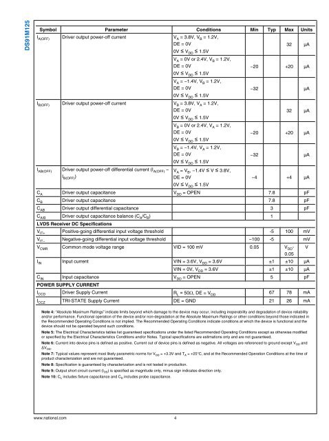
DS91M125<br />
Symbol Parameter Conditions Min Typ Max Units<br />
I A(OFF) Driver output power-off current V A = 3.8V, V B = 1.2V,<br />
DE = 0V<br />
0V ≤ V DD ≤ 1.5V<br />
V A = 0V or 2.4V, V B = 1.2V,<br />
DE = 0V<br />
0V ≤ V DD ≤ 1.5V<br />
V A = −1.4V, V B = 1.2V,<br />
DE = 0V<br />
0V ≤ V DD ≤ 1.5V<br />
I B(OFF) Driver output power-off current V B = 3.8V, V A = 1.2V,<br />
DE = 0V<br />
I AB(OFF)<br />
Driver output power-off differential current (I A(OFF) −<br />
I B(OFF) )<br />
0V ≤ V DD ≤ 1.5V<br />
V B = 0V or 2.4V, V A = 1.2V,<br />
DE = 0V<br />
0V ≤ V DD ≤ 1.5V<br />
V B = −1.4V, V A = 1.2V,<br />
DE = 0V<br />
0V ≤ V DD ≤ 1.5V<br />
V A = V B , −1.4V ≤ V ≤ 3.8V,<br />
DE = 0V<br />
0V ≤ V DD ≤ 1.5V<br />
32 µA<br />
−20 +20 µA<br />
−32 µA<br />
32 µA<br />
−20 +20 µA<br />
−32 µA<br />
−4 +4 µA<br />
C A Driver output capacitance V DD = OPEN 7.8 pF<br />
C B Driver output capacitance 7.8 pF<br />
C AB Driver output differential capacitance 3 pF<br />
C A/B Driver output capacitance balance (C A /C B ) 1<br />
LVDS Receiver DC Specifications<br />
V IT+ Positive-going differential input voltage threshold -5 100 mV<br />
V IT− Negative-going differential input voltage threshold −100 -5 mV<br />
V CMR Common mode voltage range VID = 100 mV 0.05 V DD -<br />
0.05<br />
I IN Input current VIN = 3.6V, V DD = 3.6V ±1 ±10 µA<br />
VIN = 0V, V DD = 3.6V ±1 ±10 µA<br />
C IN Input capacitance V DD = OPEN 5 pF<br />
POWER SUPPLY CURRENT<br />
ICCD Driver Supply Current RL = 50Ω, DE = VDD 67 78 mA<br />
ICCZ TRI-STATE Supply Current DE = GND 21 26 mA<br />
Note 4: “Absolute Maximum Ratings” indicate limits beyond which damage to the device may occur, including inoperability and degradation of device reliability<br />
and/or performance. Functional operation of the device and/or non-degradation at the Absolute Maximum Ratings or other conditions beyond those indicated in<br />
the Recommended Operating Conditions is not implied. The Recommended Operating Conditions indicate conditions at which the device is functional and the<br />
device should not be operated beyond such conditions.<br />
Note 5: The Electrical Characteristics tables list guaranteed specifications under the listed Recommended Operating Conditions except as otherwise modified<br />
or specified by the Electrical Characteristics Conditions and/or Notes. Typical specifications are estimations only and are not guaranteed.<br />
Note 6: Current into device pins is defined as positive. Current out of device pins is defined as negative. All voltages are referenced to ground except V OD and<br />
ΔV OD .<br />
Note 7: Typical values represent most likely parametric norms for V DD = +3.3V and T A = +25°C, and at the Recommended Operation Conditions at the time of<br />
product characterization and are not guaranteed.<br />
Note 8: Specification is guaranteed by characterization and is not tested in production.<br />
Note 9: Output short circuit current (I OS ) is specified as magnitude only, minus sign indicates direction only.<br />
Note 10: C L includes fixture capacitance and C D includes probe capacitance.<br />
www.national.com 4<br />
V