Single-Chip Low Power RF Transceiver for Narrowband Systems ...
Single-Chip Low Power RF Transceiver for Narrowband Systems ...
Single-Chip Low Power RF Transceiver for Narrowband Systems ...

Create successful ePaper yourself
Turn your PDF publications into a flip-book with our unique Google optimized e-Paper software.
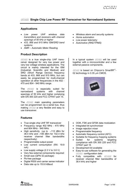
CC1021<br />
CC1021 <strong>Single</strong> <strong>Chip</strong> <strong>Low</strong> <strong>Power</strong> <strong>RF</strong> <strong>Transceiver</strong> <strong>for</strong> <strong>Narrowband</strong> <strong>Systems</strong><br />
Applications<br />
• <strong>Low</strong> power UHF wireless data<br />
transmitters and receivers with channel<br />
spacings of 50 kHz or higher<br />
• 433, 868 and 915 MHz ISM/SRD band<br />
systems<br />
• AMR – Automatic Meter Reading<br />
Product Description<br />
CC1021 is a true single-chip UHF transceiver<br />
designed <strong>for</strong> very low power and<br />
very low voltage wireless applications. The<br />
circuit is mainly intended <strong>for</strong> the ISM<br />
(Industrial, Scientific and Medical) and<br />
SRD (Short Range Device) frequency<br />
bands at 433, 868 and 915 MHz, but can<br />
easily be programmed <strong>for</strong> multi-channel<br />
operation at other frequencies in the 402 -<br />
470 and 804 - 940 MHz range.<br />
The CC1021 is especially suited <strong>for</strong><br />
narrowband systems with channel<br />
spacings of 50 kHz and higher complying<br />
with EN 300 220 and FCC CFR47 part 15.<br />
The CC1021 main operating parameters<br />
can be programmed via a serial bus, thus<br />
making CC1021 a very flexible and easy to<br />
use transceiver.<br />
Features<br />
• True single chip UHF <strong>RF</strong> transceiver<br />
• Frequency range 402 MHz - 470 MHz<br />
and 804 MHz - 940 MHz<br />
• High sensitivity (up to –112 dBm <strong>for</strong><br />
38.4 kHz and –106 dBm <strong>for</strong> 102.4 kHz<br />
receiver channel filter bandwidths<br />
respectively)<br />
• Programmable output power<br />
• <strong>Low</strong> current consumption (RX: 19.9<br />
mA)<br />
• <strong>Low</strong> supply voltage (2.3 V to 3.6 V)<br />
• Very few external components required<br />
• Small size (QFN 32 package)<br />
• Pb-free package<br />
• Digital RSSI and carrier sense indicator<br />
• Data rate up to 153.6 kBaud<br />
• Wireless alarm and security systems<br />
• Home automation<br />
• <strong>Low</strong> power telemetry<br />
• Automotive (RKE/TPMS)<br />
In a typical system CC1021 will be used<br />
together with a microcontroller and a few<br />
external passive components.<br />
CC1021 is based on <strong>Chip</strong>con’s Smart<strong>RF</strong> ® -<br />
02 technology in 0.35 µm CMOS.<br />
• OOK, FSK and GFSK data modulation<br />
• Integrated bit synchronizer<br />
• Image rejection mixer<br />
• Programmable frequency<br />
• Automatic frequency control (AFC)<br />
• Suitable <strong>for</strong> frequency hopping systems<br />
• Suited <strong>for</strong> systems targeting<br />
compliance with EN 300 220 and FCC<br />
CFR47 part 15<br />
• Development kit available<br />
• Easy-to-use software <strong>for</strong> generating the<br />
CC1021 configuration data<br />
• Fully compatible with CC1020 <strong>for</strong><br />
receiver channel filter bandwidths of<br />
38.4 kHz and higher<br />
SWRS045B Page 1 of 89
Table of Contents<br />
CC1021<br />
1. Abbreviations................................................................................................................ 4<br />
2. Absolute Maximum Ratings......................................................................................... 5<br />
3. Operating Conditions ................................................................................................... 5<br />
4. Electrical Specifications .............................................................................................. 5<br />
4.1. <strong>RF</strong> Transmit Section ............................................................................................ 6<br />
4.2. <strong>RF</strong> Receive Section ............................................................................................. 8<br />
4.3. RSSI / Carrier Sense Section ............................................................................ 11<br />
4.4. IF Section........................................................................................................... 11<br />
4.5. Crystal Oscillator Section................................................................................... 12<br />
4.6. Frequency Synthesizer Section ......................................................................... 13<br />
4.7. Digital Inputs / Outputs....................................................................................... 14<br />
4.8. Current Consumption......................................................................................... 15<br />
5. Pin Assignment........................................................................................................... 15<br />
6. Circuit Description...................................................................................................... 17<br />
7. Application Circuit...................................................................................................... 18<br />
8. Configuration Overview ............................................................................................. 21<br />
8.1. Configuration Software ...................................................................................... 21<br />
9. Microcontroller Interface............................................................................................ 22<br />
9.1. 4-wire Serial Configuration Interface ................................................................. 23<br />
9.2. Signal Interface .................................................................................................. 25<br />
10. Data Rate Programming............................................................................................. 27<br />
11. Frequency Programming ........................................................................................... 28<br />
11.1. Dithering ......................................................................................................... 29<br />
12. Receiver....................................................................................................................... 30<br />
12.1. IF Frequency .................................................................................................. 30<br />
12.2. Receiver Channel Filter Bandwidth................................................................ 30<br />
12.3. Demodulator, Bit Synchronizer and Data Decision........................................ 31<br />
12.4. Receiver Sensitivity versus Data Rate and Frequency Separation ............... 32<br />
12.5. RSSI ............................................................................................................... 33<br />
12.6. Image Rejection Calibration ........................................................................... 35<br />
12.7. Blocking and Selectivity ................................................................................. 36<br />
12.8. Linear IF Chain and AGC Settings................................................................. 38<br />
12.9. AGC Settling................................................................................................... 40<br />
12.10. Preamble Length and Sync Word .................................................................. 40<br />
12.11. Carrier Sense ................................................................................................. 41<br />
12.12. Automatic <strong>Power</strong>-up Sequencing................................................................... 41<br />
12.13. Automatic Frequency Control......................................................................... 42<br />
12.14. Digital FM ....................................................................................................... 43<br />
SWRS045B Page 2 of 89
CC1021<br />
13. Transmitter .................................................................................................................. 44<br />
13.1. FSK Modulation Formats ............................................................................... 44<br />
13.2. Output <strong>Power</strong> Programming........................................................................... 44<br />
13.3. TX Data Latency............................................................................................. 45<br />
13.4. Reducing Spurious Emission and Modulation Bandwidth.............................. 46<br />
14. Input / Output Matching and Filtering....................................................................... 46<br />
15. Frequency Synthesizer .............................................................................................. 49<br />
15.1. VCO, Charge Pump and PLL Loop Filter....................................................... 50<br />
15.2. VCO and PLL Self-Calibration ....................................................................... 51<br />
15.3. PLL Turn-on Time versus Loop Filter Bandwidth........................................... 52<br />
15.4. PLL Lock Time versus Loop Filter Bandwidth................................................ 53<br />
16. VCO and LNA Current Control .................................................................................. 53<br />
17. <strong>Power</strong> Management .................................................................................................... 54<br />
18. On-Off Keying (OOK).................................................................................................. 56<br />
19. Crystal Oscillator ........................................................................................................ 58<br />
20. Built-in Test Pattern Generator ................................................................................. 59<br />
21. Interrupt on Pin DCLK ................................................................................................ 60<br />
21.1. Interrupt upon PLL Lock................................................................................. 60<br />
21.2. Interrupt upon Received Signal Carrier Sense .............................................. 60<br />
22. PA_EN and LNA_EN Digital Output Pins ................................................................. 60<br />
22.1. Interfacing an External LNA or PA ................................................................. 60<br />
22.2. General Purpose Output Control Pins............................................................ 61<br />
22.3. PA_EN and LNA_EN Pin Drive...................................................................... 61<br />
23. System Considerations and Guidelines................................................................... 61<br />
24. PCB Layout Recommendations ................................................................................ 63<br />
25. Antenna Considerations ............................................................................................ 64<br />
26. Configuration Registers............................................................................................. 64<br />
26.1. CC1021 Register Overview............................................................................ 65<br />
27. Package Description (QFN 32) .................................................................................. 85<br />
27.1. Package Marking............................................................................................ 86<br />
27.2. Recommended PCB Footprint <strong>for</strong> Package (QFN 32)................................... 87<br />
27.3. Soldering In<strong>for</strong>mation ..................................................................................... 87<br />
27.4. Plastic Tube Specification .............................................................................. 88<br />
28. Ordering In<strong>for</strong>mation.................................................................................................. 88<br />
29. General In<strong>for</strong>mation.................................................................................................... 89<br />
SWRS045B Page 3 of 89
1. Abbreviations<br />
ACP Adjacent Channel <strong>Power</strong><br />
ACR Adjacent Channel Rejection<br />
ADC Analog-to-Digital Converter<br />
AFC Automatic Frequency Control<br />
AGC Automatic Gain Control<br />
AMR Automatic Meter Reading<br />
ASK Amplitude Shift Keying<br />
BER Bit Error Rate<br />
BOM Bill Of Materials<br />
bps bits per second<br />
BT Bandwidth-Time product (<strong>for</strong> GFSK)<br />
ChBW Receiver Channel Filter Bandwidth<br />
CW Continuous Wave<br />
DAC Digital-to-Analog Converter<br />
DNM Do Not Mount<br />
ESR Equivalent Series Resistance<br />
FHSS Frequency Hopping Spread Spectrum<br />
FM Frequency Modulation<br />
FS Frequency Synthesizer<br />
FSK Frequency Shift Keying<br />
GFSK Gaussian Frequency Shift Keying<br />
IC Integrated Circuit<br />
IF Intermediate Frequency<br />
IP3 Third Order Intercept Point<br />
ISM Industrial Scientific Medical<br />
kbps kilo bits per second<br />
LNA <strong>Low</strong> Noise Amplifier<br />
LO Local Oscillator (in receive mode)<br />
MCU Micro Controller Unit<br />
NRZ Non Return to Zero<br />
OOK On-Off Keying<br />
PA <strong>Power</strong> Amplifier<br />
PD Phase Detector / <strong>Power</strong> Down<br />
PER Packet Error Rate<br />
PCB Printed Circuit Board<br />
PN9 Pseudo-random Bit Sequence (9-bit)<br />
PLL Phase Locked Loop<br />
PSEL Program Select<br />
<strong>RF</strong> Radio Frequency<br />
RKE Remote Keyless Entry<br />
RSSI Received Signal Strength Indicator<br />
RX Receive (mode)<br />
SBW Signal Bandwidth<br />
SPI Serial Peripheral Interface<br />
SRD Short Range Device<br />
TBD To Be Decided/Defined<br />
TPMS Tire Pressure Monitoring<br />
T/R Transmit/Receive (switch)<br />
TX Transmit (mode)<br />
UHF Ultra High Frequency<br />
VCO Voltage Controlled Oscillator<br />
VGA Variable Gain Amplifier<br />
XOSC Crystal oscillator<br />
XTAL Crystal<br />
CC1021<br />
SWRS045B Page 4 of 89
2. Absolute Maximum Ratings<br />
CC1021<br />
The absolute maximum ratings given Table 1 should under no circumstances be violated.<br />
Stress exceeding one or more of the limiting values may cause permanent damage to the<br />
device.<br />
Parameter Min Max Unit Condition<br />
Supply voltage, VDD -0.3 5.0 V All supply pins must have the<br />
same voltage<br />
Voltage on any pin -0.3 VDD+0.3, max 5.0 V<br />
Input <strong>RF</strong> level 10 dBm<br />
Storage temperature range -50 150 °C<br />
Package body temperature 260 °C Norm: IPC/JEDEC J-STD-020 1<br />
Humidity non-condensing 5 85 %<br />
ESD<br />
(Human Body Model)<br />
±1<br />
±0.4<br />
kV<br />
kV<br />
Table 1. Absolute maximum ratings<br />
All pads except <strong>RF</strong><br />
<strong>RF</strong> Pads<br />
1 The reflow peak soldering temperature (body temperature) is specified according to<br />
IPC/JEDEC J-STD_020 “Moisture/Reflow Sensitivity Classification <strong>for</strong> Nonhermetic Solid<br />
State Surface Mount Devices”.<br />
Caution! ESD sensitive device.<br />
Precaution should be used when handling<br />
the device in order to prevent permanent<br />
damage.<br />
3. Operating Conditions<br />
The operating conditions <strong>for</strong> CC1021 are listed in Table 2.<br />
Parameter<br />
<strong>RF</strong> Frequency Range 402<br />
804<br />
Operating ambient temperature range<br />
Supply voltage<br />
4. Electrical Specifications<br />
Min Typ Max Unit Condition / Note<br />
470<br />
940<br />
MHz<br />
MHz<br />
-40 85 °C<br />
2.3 3.0 3.6 V<br />
Table 2. Operating conditions<br />
Programmable in
4.1. <strong>RF</strong> Transmit Section<br />
Transmit data rate<br />
Parameter<br />
Binary FSK frequency separation<br />
Output power<br />
433 MHz<br />
868 MHz<br />
Output power tolerance<br />
Harmonics, radiated CW<br />
2 nd harmonic, 433 MHz, +10 dBm<br />
3 rd harmonic, 433 MHz, +10 dBm<br />
2 nd harmonic, 868 MHz, +5 dBm<br />
3 rd harmonic, 868 MHz, +5 dBm<br />
Adjacent channel power (GFSK)<br />
433 MHz<br />
868 MHz<br />
Occupied bandwidth (99.5%,GFSK)<br />
433 MHz<br />
868 MHz<br />
Modulation bandwidth, 868 MHz<br />
19.2 kBaud, ±9.9 kHz frequency<br />
deviation<br />
38.4 kBaud, ±19.8 kHz frequency<br />
deviation<br />
CC1021<br />
Min Typ Max Unit Condition / Note<br />
0.45<br />
0<br />
0<br />
-20 to +10<br />
-20 to +5<br />
-4<br />
+3<br />
-50<br />
-50<br />
-50<br />
-50<br />
-46<br />
-42<br />
60<br />
60<br />
48<br />
106<br />
153.6 kBaud The data rate is programmable.<br />
See section 10 on page 27 <strong>for</strong><br />
details.<br />
108<br />
216<br />
kHz<br />
kHz<br />
dBm<br />
dBm<br />
dB<br />
dB<br />
dBc<br />
dBc<br />
dBc<br />
dBc<br />
dBc<br />
dBc<br />
kHz<br />
kHz<br />
kHz<br />
kHz<br />
NRZ or Manchester encoding can<br />
be used. 153.6 kBaud equals<br />
153.6 kbps using NRZ coding<br />
and 76.8 kbps using Manchester<br />
coding. See section 9.2 on page<br />
25 <strong>for</strong> details<br />
Minimum data rate <strong>for</strong> OOK is 2.4<br />
kBaud<br />
in 402 - 470 MHz range<br />
in 804 - 940 MHz range<br />
108/216 kHz is the maximum<br />
guaranteed separation at 1.84<br />
MHz reference frequency. Larger<br />
separations can be achieved at<br />
higher reference frequencies.<br />
Delivered to 50 Ω single-ended<br />
load. The output power is<br />
programmable and should not be<br />
programmed to exceed +10/+5<br />
dBm at 433/868 MHz under any<br />
operating conditions. See section<br />
14 on page 46 <strong>for</strong> details.<br />
At maximum output power<br />
At 2.3 V, +85 o C<br />
At 3.6 V, -40 o C<br />
Harmonics are measured as<br />
EIRP values according to EN 300<br />
220. The antenna (SMAFF-433<br />
and SMAFF-868 from R.W.<br />
Badland) plays a part in<br />
attenuating the harmonics.<br />
ACP is measured in a 100 kHz<br />
bandwidth at ±100 kHz offset.<br />
Modulation: 19.2 kBaud NRZ<br />
PN9 sequence, ±19.8 kHz<br />
frequency deviation.<br />
Bandwidth <strong>for</strong> 99.5% of total<br />
average power.<br />
Modulation: 19.2 kBaud NRZ<br />
PN9 sequence, ±19.8 kHz<br />
frequency deviation.<br />
Bandwidth where the power<br />
envelope of modulation equals<br />
–36 dBm. Spectrum analyzer<br />
RBW = 1 kHz.<br />
SWRS045B Page 6 of 89
Parameter<br />
Spurious emission, radiated CW<br />
47-74, 87.5-118,<br />
174-230, 470-862 MHz<br />
9 kHz – 1 GHz<br />
1 – 4 GHz<br />
Optimum load impedance<br />
433 MHz<br />
868 MHz<br />
915 MHz<br />
CC1021<br />
Min Typ Max Unit Condition / Note<br />
54 + j44<br />
15 + j24<br />
20 + j35<br />
-54<br />
-36<br />
-30<br />
dBm<br />
dBm<br />
dBm<br />
Table 3. <strong>RF</strong> transmit parameters<br />
Ω<br />
Ω<br />
Ω<br />
At maximum output power,<br />
+10/+5 dBm at 433/868 MHz.<br />
To comply with EN 300 220,<br />
FCC CFR47 part 15 and ARIB<br />
STD T-67 an external (antenna)<br />
filter, as implemented in the<br />
application circuit in Figure 25,<br />
must be used and tailored to<br />
each individual design to reduce<br />
out-of-band spurious emission<br />
levels.<br />
Spurious emissions can be<br />
measured as EIRP values<br />
according to EN 300 220. The<br />
antenna (SMAFF-433 and<br />
SMAFF-868 from R.W. Badland)<br />
plays a part in attenuating the<br />
spurious emissions.<br />
If the output power is increased<br />
using an external PA, a filter must<br />
be used to attenuate spurs below<br />
862 MHz when operating in the<br />
868 MHz frequency band in<br />
Europe. Application Note AN036<br />
CC1020/1021 Spurious Emission<br />
presents and discusses a solution<br />
that reduces the TX mode<br />
spurious emission close to 862<br />
MHz by increasing the REF_DIV<br />
from 1 to 7.<br />
Transmit mode. For matching<br />
details see section 14 on page<br />
46.<br />
SWRS045B Page 7 of 89
4.2. <strong>RF</strong> Receive Section<br />
Parameter<br />
Receiver Sensitivity, 433 MHz, FSK<br />
38.4 kHz channel filter BW (1)<br />
102.4 kHz channel filter BW (2)<br />
102.4 kHz channel filter BW (3)<br />
307.2 kHz channel filter BW (4)<br />
Receiver Sensitivity, 868 MHz, FSK<br />
38.4 kHz channel filter BW (1)<br />
102.4 kHz channel filter BW (2)<br />
102.4 kHz channel filter BW (3)<br />
307.2 kHz channel filter BW (4)<br />
Receiver sensitivity, 433 MHz, OOK<br />
9.6 kBaud<br />
153.6 kBaud<br />
Receiver sensitivity, 868 MHz, OOK<br />
9.6 kBaud<br />
153.6 kBaud<br />
Saturation (maximum input level)<br />
FSK and OOK<br />
CC1021<br />
Min Typ Max Unit Condition / Note<br />
-109<br />
-104<br />
-104<br />
-96<br />
-108<br />
-103<br />
-103<br />
-94<br />
-103<br />
-81<br />
-104<br />
-87<br />
System noise bandwidth 38.4<br />
to<br />
307.2<br />
Noise figure, cascaded<br />
433 and 868 MHz<br />
10<br />
7<br />
dBm<br />
dBm<br />
dBm<br />
dBm<br />
dBm<br />
dBm<br />
dBm<br />
dBm<br />
dBm<br />
dBm<br />
dBm<br />
dBm<br />
dBm<br />
Sensitivity is measured with PN9<br />
sequence at BER = 10 −3<br />
(1) 38.4 kHz receiver channel<br />
filter bandwidth: 4.8 kBaud, NRZ<br />
coded data, ±4.95 kHz frequency<br />
deviation.<br />
(2) 102.4 kHz receiver channel<br />
filter bandwidth: 19.2 kBaud,<br />
NRZ coded data, ±19.8 kHz<br />
frequency deviation.<br />
(3) 102.4 kHz receiver channel<br />
filter bandwidth: 38.4 kBaud, NRZ<br />
coded data, ±19.8 kHz frequency<br />
deviation.<br />
(4) 307.2 kHz receiver channel<br />
filter bandwidth: 153.6 kBaud,<br />
NRZ coded data, ±72 kHz<br />
frequency deviation.<br />
See Table 19 and Table 20 or<br />
typical sensitivity figures at other<br />
channel filter bandwidths.<br />
Sensitivity is measured with PN9<br />
sequence at BER = 10 −3<br />
Manchester coded data.<br />
See Table 27 <strong>for</strong> typical<br />
sensitivity figures at other data<br />
rates.<br />
FSK: Manchester/NRZ coded<br />
data<br />
OOK: Manchester coded data<br />
BER = 10 −3<br />
kHz The receiver channel filter 6 dB<br />
bandwidth is programmable from<br />
38.4 kHz to 307.2 kHz. See<br />
section 12.2 on page 30 <strong>for</strong><br />
details.<br />
dB<br />
NRZ coded data<br />
SWRS045B Page 8 of 89
Input IP3<br />
Parameter<br />
433 MHz 102.4 kHz channel filter BW<br />
868 MHz 102.4 kHz channel filter BW<br />
Co-channel rejection, FSK and OOK<br />
433 MHz and 868 MHz,<br />
102.4 kHz channel filter BW,<br />
Adjacent channel rejection (ACR)<br />
433 MHz 102.4 kHz channel filter BW<br />
868 MHz 102.4 kHz channel filter BW<br />
Image channel rejection<br />
433/868 MHz<br />
No I/Q gain and phase calibration<br />
I/Q gain and phase calibrated<br />
Selectivity*<br />
433 MHz 102.4 kHz channel filter BW<br />
±200 kHz offset<br />
±300 kHz offset<br />
868 MHz 102.4 kHz channel filter BW<br />
±200 kHz offset<br />
±300 kHz offset<br />
(*Close-in spurious response<br />
rejection)<br />
Blocking / Desensitization*<br />
433/868 MHz<br />
± 1 MHz<br />
± 2 MHz<br />
± 5 MHz<br />
± 10 MHz<br />
(*Out-of-band spurious response<br />
rejection)<br />
Image frequency suppression,<br />
433/868 MHz<br />
No I/Q gain and phase calibration<br />
I/Q gain and phase calibrated<br />
CC1021<br />
Min Typ Max Unit Condition / Note<br />
-23<br />
-18<br />
-16<br />
-18<br />
-15<br />
-13<br />
-11<br />
32<br />
30<br />
25/25<br />
50/50<br />
45<br />
53<br />
45<br />
50<br />
52/58<br />
56/64<br />
58/64<br />
64/66<br />
35/35<br />
60/60<br />
dBm<br />
dBm<br />
dBm<br />
dBm<br />
dBm<br />
dBm<br />
dB<br />
dB<br />
dB<br />
dB<br />
dB<br />
dB<br />
dB<br />
dB<br />
dB<br />
dB<br />
dB<br />
dB<br />
dB<br />
dB<br />
dB<br />
Two tone test (+10 MHz and +20<br />
MHz)<br />
LNA2 maximum gain<br />
LNA2 medium gain<br />
LNA2 minimum gain<br />
LNA2 maximum gain<br />
LNA2 medium gain<br />
LNA2 minimum gain<br />
Wanted signal 3 dB above the<br />
sensitivity level, CW jammer at<br />
operating frequency, BER = 10 −3<br />
Wanted signal 3 dB above the<br />
sensitivity level, CW jammer at<br />
adjacent channel, BER = 10 −3 .<br />
Measured at ±100 kHz offset.<br />
See Figure 16 to Figure 19.<br />
Wanted signal 3 dB above the<br />
sensitivity level, CW jammer at<br />
image frequency, BER = 10 −3 .<br />
102.4 kHz channel filter<br />
bandwidth. See Figure 16 to<br />
Figure 19.<br />
Image rejection after calibration<br />
will depend on temperature and<br />
supply voltage. Refer to section<br />
12.6 on page 35.<br />
Wanted signal 3 dB above the<br />
sensitivity level. CW jammer is<br />
swept in 20 kHz steps within ± 1<br />
MHz from wanted channel. BER<br />
= 10 −3 . Adjacent channel and<br />
image channel are excluded.<br />
See Figure 16 to Figure 19.<br />
Wanted signal 3 dB above the<br />
sensitivity level, CW jammer at ±<br />
1, 2, 5 and 10 MHz offset,<br />
BER = 10 −3 . 102.4 kHz channel<br />
filter bandwidth.<br />
Complying with EN 300 220,<br />
class 2 receiver requirements.<br />
Ratio between sensitivity <strong>for</strong> a<br />
signal at the image frequency to<br />
the sensitivity in the wanted<br />
channel. Image frequency is <strong>RF</strong>−<br />
2 IF. BER = 10 −3 . 102.4 kHz<br />
channel filter bandwidth.<br />
SWRS045B Page 9 of 89
Spurious reception<br />
Parameter<br />
CC1021<br />
Min Typ Max Unit Condition / Note<br />
LO leakage, 433/868 MHz
4.3. RSSI / Carrier Sense Section<br />
Parameter<br />
RSSI dynamic range<br />
RSSI accuracy ± 3<br />
CC1021<br />
Min Typ Max Unit Condition / Note<br />
RSSI linearity ± 1 dB<br />
RSSI attach time<br />
51.2 kHz channel filter BW<br />
102.4 kHz channel filter BW<br />
307.2 kHz channel filter BW<br />
Carrier sense programmable range<br />
Carrier sense at ±100 kHz and ±200<br />
kHz offset<br />
102.4 kHz channel filter BW, 433 MHz<br />
±100 kHz<br />
±200 kHz<br />
102.4 kHz channel filter BW, 868 MHz<br />
±100 kHz<br />
±200 kHz<br />
4.4. IF Section<br />
Parameter<br />
Intermediate frequency (IF)<br />
Digital channel filter bandwidth<br />
AFC resolution<br />
55 dB See section 12.5 on page 33 <strong>for</strong><br />
details.<br />
730<br />
380<br />
140<br />
dB<br />
µs<br />
µs<br />
µs<br />
See section 12.5 on page 33 <strong>for</strong><br />
details.<br />
Shorter RSSI attach times can be<br />
traded <strong>for</strong> lower RSSI accuracy.<br />
See section 12.5 on page 33 <strong>for</strong><br />
details.<br />
Shorter RSSI attach times can<br />
also be traded <strong>for</strong> reduced<br />
sensitivity and selectivity by<br />
increasing the receiver channel<br />
filter bandwidth.<br />
40 dB Accuracy is as <strong>for</strong> RSSI<br />
-57<br />
-44<br />
-60<br />
-44<br />
dBm<br />
dBm<br />
dBm<br />
dBm<br />
Table 5. RSSI / Carrier sense parameters<br />
At carrier sense level −98 dBm,<br />
CW jammer at ±100 kHz and<br />
±200 kHz offset.<br />
Carrier sense is measured by<br />
applying a signal at ±100 kHz and<br />
±200 kHz offset and observe at<br />
which level carrier sense is<br />
indicated.<br />
Min Typ Max Unit Condition / Note<br />
307.2 kHz See section 12.1 on page 30 <strong>for</strong><br />
details.<br />
38.4<br />
to<br />
307.2<br />
kHz<br />
1200 Hz<br />
Table 6. IF section parameters<br />
The channel filter 6 dB bandwidth<br />
is programmable from 9.6 kHz to<br />
307.2 kHz. See section 12.2 on<br />
page 30 <strong>for</strong> details.<br />
At 19.2 kBaud<br />
Given as Baud rate/16. See<br />
section 12.13 on page 42 <strong>for</strong><br />
details.<br />
SWRS045B Page 11 of 89
4.5. Crystal Oscillator Section<br />
Parameter<br />
Crystal Oscillator Frequency<br />
Crystal operation<br />
Crystal load capacitance<br />
CC1021<br />
Min Typ Max Unit Condition / Note<br />
4.9152 14.7456 19.6608 MHz Recommended frequency is<br />
14.7456 MHz. See section 19 on<br />
page 58 <strong>for</strong> details.<br />
12<br />
12<br />
12<br />
Parallel<br />
22<br />
16<br />
16<br />
Crystal oscillator start-up time 1.55<br />
1.0<br />
0.90<br />
0.95<br />
0.60<br />
0.63<br />
External clock signal drive,<br />
sine wave<br />
External clock signal drive,<br />
full-swing digital external clock<br />
300<br />
0 - VDD<br />
30<br />
30<br />
16<br />
pF<br />
pF<br />
pF<br />
ms<br />
ms<br />
ms<br />
ms<br />
ms<br />
ms<br />
mVpp<br />
Table 7. Crystal oscillator parameters<br />
V<br />
C4 and C5 are loading<br />
capacitors. See section 19 on<br />
page 58 <strong>for</strong> details.<br />
4.9-6 MHz, 22 pF recommended<br />
6-8 MHz, 16 pF recommended<br />
8-19.6 MHz, 16 pF recommended<br />
4.9152 MHz, 12 pF load<br />
7.3728 MHz, 12 pF load<br />
9.8304 MHz, 12 pF load<br />
14.7456 MHz, 16 pF load<br />
17.2032 MHz, 12 pF load<br />
19.6608 MHz, 12 pF load<br />
The external clock signal must be<br />
connected to XOSC_Q1 using a<br />
DC block (10 nF). Set<br />
XOSC_BYPASS = 0 in the<br />
INTE<strong>RF</strong>ACE register when using<br />
an external clock signal with low<br />
amplitude or a crystal.<br />
The external clock signal must be<br />
connected to XOSC_Q1. No DC<br />
block shall be used. Set<br />
XOSC_BYPASS = 1 in the<br />
INTE<strong>RF</strong>ACE register when using<br />
a full-swing digital external clock.<br />
SWRS045B Page 12 of 89
4.6. Frequency Synthesizer Section<br />
Parameter<br />
Phase noise, 402 – 470 MHz<br />
Phase noise, 804 – 940 MHz<br />
PLL loop filter bandwidth<br />
Loop filter 2, up to 19.2 kBaud<br />
Loop filter 3, up to 38.4 kBaud<br />
PLL lock time (RX / TX turn time)<br />
Loop filter 2, up to 19.2 kBaud<br />
Loop filter 3, up to 38.4 kBaud<br />
Loop filter 5, up to 153.6 kBaud<br />
PLL turn-on time. From power down<br />
mode with crystal oscillator running.<br />
Loop filter 2, up to 19.2 kBaud<br />
Loop filter 3, up to 38.4 kBaud<br />
Loop filter 5, up to 153.6 kBaud<br />
CC1021<br />
Min Typ Max Unit Condition / Note<br />
-79<br />
-80<br />
-87<br />
-100<br />
-105<br />
-73<br />
-74<br />
-81<br />
-94<br />
-111<br />
15<br />
30.5<br />
140<br />
75<br />
14<br />
1300<br />
1080<br />
700<br />
dBc/Hz<br />
dBc/Hz<br />
dBc/Hz<br />
dBc/Hz<br />
dBc/Hz<br />
dBc/Hz<br />
dBc/Hz<br />
dBc/Hz<br />
dBc/Hz<br />
dBc/Hz<br />
kHz<br />
kHz<br />
Table 8. Frequency synthesizer parameters<br />
us<br />
us<br />
us<br />
us<br />
us<br />
us<br />
Unmodulated carrier<br />
At 12.5 kHz offset from carrier<br />
At 25 kHz offset from carrier<br />
At 50 kHz offset from carrier<br />
At 100 kHz offset from carrier<br />
At 1 MHz offset from carrier<br />
Measured using loop filter<br />
components given in Table 13.<br />
The phase noise will be higher <strong>for</strong><br />
larger PLL loop filter bandwidth.<br />
After PLL and VCO calibration.<br />
The PLL loop bandwidth is<br />
programmable.<br />
See Table 25 on page 52 <strong>for</strong> loop<br />
filter component values.<br />
307.2 kHz frequency step to <strong>RF</strong><br />
frequency within ±10 kHz, ±15<br />
kHz, ±50 kHz settling accuracy<br />
<strong>for</strong> loop filter 2, 3 and 5<br />
respectively. Depends on loop<br />
filter component values and<br />
PLL_BW register setting. See<br />
Table 26 on page 53 <strong>for</strong> more<br />
details.<br />
Time from writing to registers to<br />
<strong>RF</strong> frequency within ±10 kHz, ±15<br />
kHz, ±50 kHz settling accuracy<br />
<strong>for</strong> loop filter 2, 3 and 5<br />
respectively. Depends on loop<br />
filter component values and<br />
PLL_BW register setting. See<br />
Table 25 on page 53 <strong>for</strong> more<br />
details.<br />
SWRS045B Page 13 of 89
4.7. Digital Inputs / Outputs<br />
Parameter<br />
Logic "0" input voltage<br />
Logic "1" input voltage<br />
CC1021<br />
Min Typ Max Unit Condition / Note<br />
0 0.3*<br />
VDD<br />
0.7*<br />
VDD<br />
Logic "0" output voltage 0<br />
Logic "1" output voltage 2.5<br />
Logic "0" input current<br />
Logic "1" input current<br />
V<br />
VDD V<br />
0.4 V Output current −2.0 mA,<br />
3.0 V supply voltage<br />
VDD V Output current 2.0 mA,<br />
3.0 V supply voltage<br />
NA −1 µA Input signal equals GND.<br />
PSEL has an internal pull-up<br />
resistor and during configuration<br />
the current will be -350 µA.<br />
NA 1 µA Input signal equals VDD<br />
DIO setup time 20 ns TX mode, minimum time DIO<br />
must be ready be<strong>for</strong>e the positive<br />
edge of DCLK. Data should be<br />
set up on the negative edge of<br />
DCLK.<br />
DIO hold time<br />
Serial interface (PCLK, PDI, PDO<br />
and PSEL) timing specification<br />
Pin drive, LNA_EN, PA_EN<br />
10 ns TX mode, minimum time DIO<br />
must be held after the positive<br />
edge of DCLK. Data should be<br />
set up on the negative edge of<br />
DCLK.<br />
0.90<br />
0.87<br />
0.81<br />
0.69<br />
0.93<br />
0.92<br />
0.89<br />
0.79<br />
mA<br />
mA<br />
mA<br />
mA<br />
mA<br />
mA<br />
mA<br />
mA<br />
Table 9. Digital inputs / outputs parameters<br />
See Table 14 on page 24 <strong>for</strong><br />
more details<br />
Source current<br />
0 V on LNA_EN, PA_EN pins<br />
0.5 V on LNA_EN, PA_EN pins<br />
1.0 V on LNA_EN, PA_EN pins<br />
1.5 V on LNA_EN, PA_EN pins<br />
Sink current<br />
3.0 V on LNA_EN, PA_EN pins<br />
2.5 V on LNA_EN, PA_EN pins<br />
2.0 V on LNA_EN, PA_EN pins<br />
1.5 V on LNA_EN, PA_EN pins<br />
See Figure 35 on page 61 <strong>for</strong><br />
more details.<br />
SWRS045B Page 14 of 89
4.8. Current Consumption<br />
Parameter<br />
<strong>Power</strong> Down mode<br />
Current Consumption,<br />
receive mode 433 and 868 MHz<br />
Current Consumption,<br />
transmit mode 433/868 MHz:<br />
P = −20 dBm<br />
P = −5 dBm<br />
P = 0 dBm<br />
P = +5 dBm<br />
P = +10 dBm (433 MHz only)<br />
Current Consumption, crystal<br />
oscillator<br />
Current Consumption, crystal<br />
oscillator and bias<br />
Current Consumption, crystal<br />
oscillator, bias and synthesizer<br />
5. Pin Assignment<br />
Table 11 provides an overview of the<br />
CC1021 pinout.<br />
CC1021<br />
Min Typ Max Unit Condition / Note<br />
0.2 1.8 µA Oscillator core off<br />
19.9 mA<br />
12.3/14.5<br />
14.4/17.0<br />
16.2/20.5<br />
20.5/25.1<br />
27.1<br />
77<br />
500<br />
7.5<br />
mA<br />
mA<br />
mA<br />
mA<br />
mA<br />
µA<br />
µA<br />
mA<br />
Table 10. Current consumption<br />
PCLK 1 24 VC<br />
PDI 2<br />
PDO 3<br />
DGND 4<br />
DVDD 5<br />
DGND 6<br />
DCLK 7<br />
DIO 8<br />
AGND<br />
AD_REF<br />
AVDD<br />
CHP_OUT<br />
AVDD<br />
DGND<br />
DVDD<br />
PSEL<br />
25<br />
26<br />
27<br />
28<br />
29<br />
30<br />
31<br />
32<br />
16<br />
15<br />
14<br />
13<br />
12<br />
11<br />
10<br />
9<br />
AVDD<br />
PA_EN<br />
LNA_EN<br />
AVDD<br />
AVDD<br />
XOSC_Q2<br />
XOSC_Q1<br />
LOCK<br />
The output power is delivered to<br />
a 50 Ω single-ended load.<br />
See section 13.2 on page 44 <strong>for</strong><br />
more details.<br />
14.7456 MHz, 16 pF load crystal<br />
14.7456 MHz, 16 pF load crystal<br />
14.7456 MHz, 16 pF load crystal<br />
The CC1021 comes in a QFN32 type<br />
package (see page 85 <strong>for</strong> details).<br />
23 AVDD<br />
22 AVDD<br />
21 <strong>RF</strong>_OUT<br />
20 AVDD<br />
19 <strong>RF</strong>_IN<br />
18 AVDD<br />
17 R_BIAS<br />
AGND<br />
Exposed die<br />
attached pad<br />
Figure 1. CC1021 package (top view)<br />
SWRS045B Page 15 of 89
CC1021<br />
Pin no. Pin name Pin type Description<br />
- AGND Ground (analog) Exposed die attached pad. Must be soldered to a solid ground plane as<br />
this is the ground connection <strong>for</strong> all analog modules. See page 63 <strong>for</strong><br />
more details.<br />
1 PCLK Digital input Programming clock <strong>for</strong> SPI configuration interface<br />
2 PDI Digital input Programming data input <strong>for</strong> SPI configuration interface<br />
3 PDO Digital output Programming data output <strong>for</strong> SPI configuration interface<br />
4 DGND Ground (digital) Ground connection (0 V) <strong>for</strong> digital modules and digital I/O<br />
5 DVDD <strong>Power</strong> (digital) <strong>Power</strong> supply (3 V typical) <strong>for</strong> digital modules and digital I/O<br />
6 DGND Ground (digital) Ground connection (0 V) <strong>for</strong> digital modules (substrate)<br />
7 DCLK Digital output Clock <strong>for</strong> data in both receive and transmit mode.<br />
Can be used as receive data output in asynchronous mode<br />
8 DIO Digital input/output Data input in transmit mode; data output in receive mode<br />
Can also be used to start power-up sequencing in receive<br />
9 LOCK Digital output PLL Lock indicator, active low. Output is asserted (low) when PLL is in<br />
lock. The pin can also be used as a general digital output, or as receive<br />
data output in synchronous NRZ/Manchester mode<br />
10 XOSC_Q1 Analog input Crystal oscillator or external clock input<br />
11 XOSC_Q2 Analog output Crystal oscillator<br />
12 AVDD <strong>Power</strong> (analog) <strong>Power</strong> supply (3 V typical) <strong>for</strong> crystal oscillator<br />
13 AVDD <strong>Power</strong> (analog) <strong>Power</strong> supply (3 V typical) <strong>for</strong> the IF VGA<br />
14 LNA_EN Digital output General digital output. Can be used <strong>for</strong> controlling an external LNA if<br />
higher sensitivity is needed.<br />
15 PA_EN Digital output General digital output. Can be used <strong>for</strong> controlling an external PA if<br />
higher output power is needed.<br />
16 AVDD <strong>Power</strong> (analog) <strong>Power</strong> supply (3 V typical) <strong>for</strong> global bias generator and IF anti-alias<br />
filter<br />
17 R_BIAS Analog output Connection <strong>for</strong> external precision bias resistor (82 kΩ, ± 1%)<br />
18 AVDD <strong>Power</strong> (analog) <strong>Power</strong> supply (3 V typical) <strong>for</strong> LNA input stage<br />
19 <strong>RF</strong>_IN <strong>RF</strong> Input <strong>RF</strong> signal input from antenna (external AC-coupling)<br />
20 AVDD <strong>Power</strong> (analog) <strong>Power</strong> supply (3 V typical) <strong>for</strong> LNA<br />
21 <strong>RF</strong>_OUT <strong>RF</strong> output <strong>RF</strong> signal output to antenna<br />
22 AVDD <strong>Power</strong> (analog) <strong>Power</strong> supply (3 V typical) <strong>for</strong> LO buffers, mixers, prescaler, and first PA<br />
stage<br />
23 AVDD <strong>Power</strong> (analog) <strong>Power</strong> supply (3 V typical) <strong>for</strong> VCO<br />
24 VC Analog input VCO control voltage input from external loop filter<br />
25 AGND Ground (analog) Ground connection (0 V) <strong>for</strong> analog modules (guard)<br />
26 AD_REF <strong>Power</strong> (analog) 3 V reference input <strong>for</strong> ADC<br />
27 AVDD <strong>Power</strong> (analog) <strong>Power</strong> supply (3 V typical) <strong>for</strong> charge pump and phase detector<br />
28 CHP_OUT Analog output PLL charge pump output to external loop filter<br />
29 AVDD <strong>Power</strong> (analog) <strong>Power</strong> supply (3 V typical) <strong>for</strong> ADC<br />
30 DGND Ground (digital) Ground connection (0 V) <strong>for</strong> digital modules (guard)<br />
31 DVDD <strong>Power</strong> (digital) <strong>Power</strong> supply connection (3 V typical) <strong>for</strong> digital modules<br />
32 PSEL Digital input Programming chip select, active low, <strong>for</strong> configuration interface. Internal<br />
pull-up resistor.<br />
Note:<br />
DCLK, DIO and LOCK are highimpedance<br />
(3-state) in power down<br />
(BIAS_PD = 1 in the MAIN register).<br />
Table 11. Pin assignment overview<br />
The exposed die attached pad must be<br />
soldered to a solid ground plane as this is<br />
the main ground connection <strong>for</strong> the chip.<br />
SWRS045B Page 16 of 89
6. Circuit Description<br />
<strong>RF</strong>_IN LNA<br />
<strong>RF</strong>_OUT<br />
PA<br />
LNA 2<br />
<strong>Power</strong><br />
Control<br />
PA_EN LNA_EN<br />
Multiplexer<br />
BIAS<br />
0<br />
:2<br />
90<br />
Multiplexer<br />
A simplified block diagram of CC1021 is<br />
shown in Figure 2. Only signal pins are<br />
shown.<br />
CC1021 features a low-IF receiver. The<br />
received<br />
<strong>RF</strong> signal is amplified by the low-<br />
noise<br />
amplifier (LNA and LNA2) and<br />
down-converted in quadrature (I and Q) to<br />
the intermediate frequency (IF). At IF, the<br />
I/Q signal is complex filtered and<br />
amplified, and then digitized by the ADCs.<br />
Automatic gain control, fine channel<br />
filtering, demodulation and bit<br />
synchronization is per<strong>for</strong>med digitally.<br />
CC1021 outputs the digital demodulated<br />
data on the DIO pin. A synchronized data<br />
clock is available at the DCLK pin. RSSI is<br />
available in digital <strong>for</strong>mat and can be read<br />
via the serial interface. The RSSI also<br />
features a programmable carrier sense<br />
indicator.<br />
In transmit mode, the synthesized <strong>RF</strong><br />
frequency is fed directly to the power<br />
0<br />
90 :2<br />
XOSC<br />
R_BIAS XOSC_Q1 XOSC_Q2<br />
ADC<br />
ADC<br />
FREQ<br />
SYNTH<br />
VC CHP_OUT<br />
Figure 2. CC1021 simplified<br />
block diagram<br />
DIGITAL<br />
DEMODULATOR<br />
- Digital RSSI<br />
- Gain Control<br />
- Image Suppression<br />
- Channel Filtering<br />
- Demodulation<br />
CONTROL<br />
LOGIC<br />
DIGITAL<br />
MODULATOR<br />
- Modulation<br />
- Data shaping<br />
- <strong>Power</strong> Control<br />
CC1021<br />
DIGITAL<br />
INTE<strong>RF</strong>ACE<br />
TO µC<br />
LOCK<br />
DIO<br />
DCLK<br />
PDO<br />
PDI<br />
PCLK<br />
PSEL<br />
amplifier (PA). The <strong>RF</strong> output is frequency<br />
shift keyed (FSK) by the digital bit stream<br />
that is fed to the DIO pin. Optionally, a<br />
Gaussian filter can be used to obtain<br />
Gaussian FSK (GFSK).<br />
The frequency synthesizer includes a<br />
completely on-chip LC VCO and a 90<br />
degrees phase splitter <strong>for</strong> generating the<br />
LO_I and LO_Q signals to the downconversion<br />
mixers in receive mode. The<br />
VCO operates in the frequency range<br />
1.608-1.880 GHz. The CHP_OUT pin is<br />
the charge pump output and VC is the<br />
control node of the on-chip VCO. The<br />
external loop filter is placed between these<br />
pins. A crystal is to be connected between<br />
XOSC_Q1 and XOSC_Q2. A lock signal is<br />
available from the PLL.<br />
The 4-wire SPI serial interface is used <strong>for</strong><br />
configuration.<br />
SWRS045B Page 17 of 89
7. Application Circuit<br />
Very few external components are<br />
required <strong>for</strong> the operation of CC1021. The<br />
recommended application circuit is shown<br />
in Figure 3. The external components are<br />
described in Table 12 and values are<br />
given in Table 13.<br />
Input / output matching<br />
L1 and C1 is the input match <strong>for</strong> the<br />
receiver. L1 is also a DC choke <strong>for</strong><br />
biasing. L2 and C3 are used to match the<br />
transmitter to 50 Ω. Internal circuitry<br />
makes it possible to connect the input and<br />
output together and match the CC1021 to<br />
50 Ω in both RX and TX mode. However, it<br />
is recommended to use an external T/R<br />
switch <strong>for</strong> optimum per<strong>for</strong>mance. See<br />
section 14 on page 46 <strong>for</strong> details.<br />
Component values <strong>for</strong> the matching<br />
network are easily found using the<br />
Smart<strong>RF</strong> ® Studio software.<br />
Bias resistor<br />
The precision bias resistor R1 is used to<br />
set an accurate bias current.<br />
PLL loop filter<br />
The loop filter consists of two resistors (R2<br />
and R3) and three capacitors (C6-C8). C7<br />
and C8 may be omitted in applications<br />
CC1021<br />
where high loop bandwidth is desired. The<br />
values shown in Table 13 are optimized<br />
<strong>for</strong> 38.4 kBaud data rate. Component<br />
values <strong>for</strong> other data rates are easily found<br />
using the Smart<strong>RF</strong> ® Studio software.<br />
Crystal<br />
An external crystal with two loading<br />
capacitors (C4 and C5) is used <strong>for</strong> the<br />
crystal oscillator. See section 19 on page<br />
58 <strong>for</strong> details.<br />
Additional filtering<br />
Additional external components (e.g. <strong>RF</strong><br />
LC or SAW filter) may be used in order to<br />
improve the per<strong>for</strong>mance in specific<br />
applications. See section 14 on page 46<br />
<strong>for</strong> further in<strong>for</strong>mation.<br />
<strong>Power</strong> supply decoupling and filtering<br />
<strong>Power</strong> supply decoupling and filtering<br />
must be used (not shown in the application<br />
circuit). The placement and size of the<br />
decoupling capacitors and the power<br />
supply filtering are very important to<br />
achieve the optimum per<strong>for</strong>mance <strong>for</strong><br />
narrowband applications. <strong>Chip</strong>con<br />
provides a reference design that should be<br />
followed very closely.<br />
Ref Description<br />
C1 LNA input match and DC block, see page 46<br />
C3 PA output match and DC block, see page 46<br />
C4 Crystal load capacitor, see page 58<br />
C5 Crystal load capacitor, see page 58<br />
C6 PLL loop filter capacitor<br />
C7 PLL loop filter capacitor (may be omitted <strong>for</strong> highest loop bandwidth)<br />
C8 PLL loop filter capacitor (may be omitted <strong>for</strong> highest loop bandwidth)<br />
C60 Decoupling capacitor<br />
L1 LNA match and DC bias (ground), see page 46<br />
L2 PA match and DC bias (supply voltage), see page 46<br />
R1 Precision resistor <strong>for</strong> current reference generator<br />
R2 PLL loop filter resistor<br />
R3 PLL loop filter resistor<br />
R10 PA output match, see page 46<br />
XTAL Crystal, see page 58<br />
Table 12. Overview of external components (excluding supply decoupling capacitors)<br />
SWRS045B Page 18 of 89
Microcontroller configuration interface and signal interface<br />
DVDD=3V<br />
1<br />
2<br />
3<br />
4<br />
5<br />
6<br />
7<br />
8<br />
PCLK<br />
PDI<br />
PDO<br />
DGND<br />
DVDD<br />
DGND<br />
DCLK<br />
DIO<br />
DVDD=3V<br />
32<br />
PSEL<br />
LOCK<br />
9<br />
31 DVDD DVDD<br />
CC1021 CC1021<br />
XOSC_Q1<br />
10<br />
C4<br />
30<br />
DGND<br />
XOSC_Q2<br />
XTAL<br />
AVDD=3V<br />
11<br />
29<br />
AVDD<br />
AVDD<br />
C5<br />
12<br />
28<br />
CHP_OUT CHP_OUT<br />
AVDD<br />
13<br />
27<br />
AVDD<br />
LNA_EN<br />
14<br />
26<br />
AD_REF<br />
PA_EN<br />
15<br />
25<br />
AGND<br />
AVDD<br />
16<br />
VC<br />
AVDD<br />
AVDD<br />
<strong>RF</strong>_OUT<br />
AVDD<br />
<strong>RF</strong>_IN<br />
AVDD<br />
R_BIAS<br />
AVDD=3V<br />
24<br />
23<br />
22<br />
21<br />
20<br />
19<br />
18<br />
17<br />
C7 R3<br />
C8<br />
AVDD=3V<br />
R1<br />
R2<br />
AVDD=3V<br />
AVDD=3V<br />
R10<br />
L2<br />
L1<br />
C6<br />
C60<br />
C3<br />
C1<br />
CC1021<br />
LC Filter<br />
Figure 3. Typical application and test circuit (power supply decoupling not shown)<br />
Item 433 MHz 868 MHz 915 MHz<br />
C1 10 pF, 5%, NP0, 0402 47 pF, 5%, NP0, 0402 47 pF, 5%, NP0, 0402<br />
C3 5.6 pF, 5%, NP0, 0402 10 pF, 5%, NP0, 0402 10 pF, 5%, NP0, 0402<br />
C4 22 pF, 5%, NP0, 0402 22 pF, 5%, NP0, 0402 22 pF, 5%, NP0, 0402<br />
C5 12 pF, 5%, NP0, 0402 12 pF, 5%, NP0, 0402 12 pF, 5%, NP0, 0402<br />
C6 3.9 nF, 10%, X7R, 0603 3.9 nF, 10%, X7R, 0603 3.9 nF, 10%, X7R, 0603<br />
C7 120 pF, 10%, X7R, 0402 120 pF, 10%, X7R, 0402 120 pF, 10%, X7R, 0402<br />
C8 33 pF, 10%, X7R, 0402 33 pF, 10%, X7R, 0402 33 pF, 10%, X7R, 0402<br />
C60 220 pF, 5%, NP0, 0402 220 pF, 5%, NP0, 0402 220 pF, 5%, NP0, 0402<br />
L1 33 nH, 5%, 0402 82 nH, 5%, 0402 82 nH, 5%, 0402<br />
L2 22 nH, 5%, 0402 3.6 nH, 5%, 0402 3.6 nH, 5%, 0402<br />
R1 82 kΩ, 1%, 0402 82 kΩ, 1%, 0402 82 kΩ, 1%, 0402<br />
R2 12 kΩ, 5%, 0402 12 kΩ, 5%, 0402 12 kΩ, 5%, 0402<br />
R3 39 kΩ, 5%, 0402 39 kΩ, 5%, 0402 39 kΩ, 5%, 0402<br />
R10 82 Ω, 5%, 0402 82 Ω, 5%, 0402 82 Ω, 5%, 0402<br />
XTAL 14.7456 MHz crystal, 14.7456 MHz crystal, 14.7456 MHz crystal,<br />
16 pF load<br />
16 pF load<br />
16 pF load<br />
Note: Items shaded vary <strong>for</strong> different frequencies.<br />
Table 13. Bill of materials <strong>for</strong> the application circuit in Figure 3. The PLL loop filter is<br />
optimized <strong>for</strong> 38.4 kBaud data rate.<br />
Note:<br />
The PLL loop filter component values in<br />
Table 13 (R2, R3, C6-C8) are optimized<br />
<strong>for</strong> 38.4 kBaud data rate. The Smart<strong>RF</strong> ®<br />
Studio software provides component<br />
values <strong>for</strong> other data rates using the<br />
equations on page 50.<br />
Monopole<br />
antenna<br />
(50 Ohm)<br />
T/R Switch<br />
In the CC1020EMX reference design,<br />
which is also applicable <strong>for</strong> CC1021,<br />
LQG15HS series inductors from Murata<br />
have been used. The switch is SW-456<br />
from M/A-COM.<br />
SWRS045B Page 19 of 89
The LC filter in Figure 3 is inserted in the<br />
TX path only. The filter will reduce the<br />
emission of harmonics and the spurious<br />
emissions in the TX path. An alternative is<br />
to insert the LC filter between the antenna<br />
and the T/R switch as shown in Figure 4.<br />
Microcontroller configuration interface and signal interface<br />
DVDD=3V<br />
1<br />
2<br />
3<br />
4<br />
5<br />
6<br />
7<br />
8<br />
PCLK<br />
PDI<br />
PDO<br />
DGND<br />
DVDD<br />
DGND<br />
DCLK<br />
DIO<br />
DVDD=3V<br />
32<br />
PSEL<br />
LOCK<br />
9<br />
31 DVDD<br />
CC1021 CC1021<br />
XOSC_Q1<br />
10<br />
C4<br />
30<br />
DGND<br />
XOSC_Q2<br />
XTAL<br />
AVDD=3V<br />
11<br />
29<br />
AVDD<br />
AVDD<br />
C5<br />
12<br />
28<br />
CHP_OUT CHP_OUT<br />
AVDD<br />
13<br />
27<br />
AVDD<br />
LNA_EN<br />
14<br />
26<br />
AD_REF<br />
PA_EN<br />
15<br />
25<br />
AGND<br />
AVDD<br />
16<br />
CC1021<br />
The filter will reduce the emission of<br />
harmonics and the spurious emissions in<br />
the TX path as well as increase the<br />
receiver selectivity. The sensitivity will be<br />
slightly reduced due to the insertion loss of<br />
the LC filter.<br />
VC<br />
AVDD<br />
AVDD<br />
<strong>RF</strong>_OUT<br />
AVDD<br />
<strong>RF</strong>_IN<br />
AVDD<br />
R_BIAS<br />
AVDD=3V<br />
24<br />
23<br />
22<br />
21<br />
20<br />
19<br />
18<br />
17<br />
C7 R3<br />
C8<br />
AVDD=3V<br />
R1<br />
R2<br />
AVDD=3V<br />
AVDD=3V<br />
R10<br />
L2<br />
L1<br />
C6<br />
C60<br />
C3<br />
C1<br />
T/R Switch<br />
Figure 4. Alternative application circuit (power supply decoupling not shown)<br />
Monopole<br />
antenna<br />
(50 Ohm)<br />
LC Filter<br />
SWRS045B Page 20 of 89
8. Configuration Overview<br />
CC1021 can be configured to achieve the<br />
optimum per<strong>for</strong>mance <strong>for</strong> different<br />
applications. Through the programmable<br />
configuration registers the following key<br />
parameters can be programmed:<br />
• Receive / transmit mode<br />
• <strong>RF</strong> output power<br />
• Frequency synthesizer key parameters:<br />
<strong>RF</strong> output frequency, FSK frequency<br />
8.1. Configuration Software<br />
<strong>Chip</strong>con provides users of CC1021 with a<br />
software program, Smart<strong>RF</strong> ® Studio<br />
(Windows interface) that generates all<br />
necessary CC1021 configuration data<br />
based on the user's selections of various<br />
parameters. These hexadecimal numbers<br />
will then be the necessary input to the<br />
microcontroller <strong>for</strong> the configuration of<br />
Figure 5. Smart<strong>RF</strong> ® Studio user interface<br />
CC1021<br />
separation, crystal oscillator reference<br />
frequency<br />
• <strong>Power</strong>-down / power-up mode<br />
• Crystal oscillator power-up / powerdown<br />
• Data rate and data <strong>for</strong>mat (NRZ,<br />
Manchester coded or UART interface)<br />
• Synthesizer lock indicator mode<br />
• Digital RSSI and carrier sense<br />
• FSK / GFSK / OOK modulation<br />
CC1021. In addition, the program will<br />
provide the user with the component<br />
values needed <strong>for</strong> the input/output<br />
matching circuit, the PLL loop filter and the<br />
LC filter.<br />
Figure 5 shows the user interface of the<br />
CC1021 configuration software.<br />
Note: The CC1020/1070DK Development Kit with a fully assembled CC1020EMX Evaluation<br />
Module together with the CC1021 specific software should be used <strong>for</strong> evaluation of the CC1021<br />
transceiver.<br />
SWRS045B Page 21 of 89
9. Microcontroller Interface<br />
Used in a typical system, CC1021 will<br />
interface to a microcontroller. This<br />
microcontroller must be able to:<br />
• Program CC1021 into different modes via<br />
the 4-wire serial configuration interface<br />
(PDI, PDO, PCLK and PSEL)<br />
• Interface to the bi-directional<br />
synchronous data signal interface (DIO<br />
and DCLK)<br />
• Optionally, the microcontroller can do<br />
data encoding / decoding<br />
• Optionally, the microcontroller can<br />
monitor the LOCK pin <strong>for</strong> frequency<br />
lock status, carrier sense status or<br />
other status in<strong>for</strong>mation.<br />
• Optionally, the microcontroller can read<br />
back the digital RSSI value and other<br />
status in<strong>for</strong>mation via the 4-wire serial<br />
interface<br />
Configuration interface<br />
The microcontroller interface is shown in<br />
Figure 6. The microcontroller uses 3 or 4<br />
I/O pins <strong>for</strong> the configuration interface<br />
(PDI, PDO, PCLK and PSEL). PDO should<br />
be connected to a microcontroller input.<br />
PDI, PCLK and PSEL must be<br />
microcontroller outputs. One I/O pin can<br />
be saved if PDI and PDO are connected<br />
together and a bi-directional pin is used at<br />
the microcontroller.<br />
CC1021<br />
The microcontroller pins connected to PDI,<br />
PDO and PCLK can be used <strong>for</strong> other<br />
purposes when the configuration interface<br />
is not used. PDI, PDO and PCLK are high<br />
impedance inputs as long as PSEL is not<br />
activated (active low).<br />
PSEL has an internal pull-up resistor and<br />
should be left open (tri-stated by the<br />
microcontroller) or set to a high level<br />
during power down mode in order to<br />
prevent a trickle current flowing in the pullup.<br />
Signal interface<br />
A bi-directional pin is usually used <strong>for</strong> data<br />
(DIO) to be transmitted and data received.<br />
DCLK providing the data timing should be<br />
connected to a microcontroller input.<br />
As an option, the data output in receive<br />
mode can be made available on a<br />
separate pin. See section 9.2 on page <strong>for</strong><br />
25 further details.<br />
PLL lock signal<br />
Optionally, one microcontroller pin can be<br />
used to monitor the LOCK signal. This<br />
signal is at low logic level when the PLL is<br />
in lock. It can also be used <strong>for</strong> carrier<br />
sense and to monitor other internal test<br />
signals.<br />
PCLK<br />
PDI<br />
PDO (Optional)<br />
PSEL<br />
Microcontroller<br />
DIO<br />
DCLK<br />
LOCK<br />
(Optional)<br />
Figure 6. Microcontroller interface<br />
SWRS045B Page 22 of 89
9.1. 4-wire Serial Configuration Interface<br />
CC1021 is configured via a simple 4-wire<br />
SPI-compatible interface (PDI, PDO,<br />
PCLK and PSEL) where CC1021 is the<br />
slave. There are 8-bit configuration<br />
registers, each addressed by a 7-bit<br />
address. A Read/Write bit initiates a read<br />
or write operation. A full configuration of<br />
CC1021 requires sending 33 data frames of<br />
16 bits each (7 address bits, R/W bit and 8<br />
data bits). The time needed <strong>for</strong> a full<br />
configuration depends on the PCLK<br />
frequency. With a PCLK frequency of 10<br />
MHz the full configuration is done in less<br />
than 53 µs. Setting the device in power<br />
down mode requires sending one frame<br />
only and will in this case take less than 2<br />
µs. All registers are also readable.<br />
During each write-cycle, 16 bits are sent<br />
on the PDI-line. The seven most<br />
significant bits of each data frame (A6:0)<br />
are the address-bits. A6 is the MSB (Most<br />
Significant Bit) of the address and is sent<br />
as the first bit. The next bit is the R/W bit<br />
(high <strong>for</strong> write, low <strong>for</strong> read). The 8 databits<br />
are then transferred (D7:0). During<br />
address and data transfer the PSEL<br />
(Program SELect) must be kept low. See<br />
Figure 7.<br />
The timing <strong>for</strong> the programming is also<br />
shown in Figure 7 with reference to Table<br />
PCLK<br />
PDI<br />
PDO<br />
PSEL<br />
T SS<br />
T CL,min<br />
T CH,min<br />
Address Write mode<br />
CC1021<br />
14. The clocking of the data on PDI is<br />
done on the positive edge of PCLK. Data<br />
should be set up on the negative edge of<br />
PCLK by the microcontroller. When the<br />
last bit, D0, of the 8 data-bits has been<br />
loaded, the data word is loaded into the<br />
internal configuration register.<br />
The configuration data will be retained<br />
during a programmed power down mode,<br />
but not when the power supply is turned<br />
off. The registers can be programmed in<br />
any order.<br />
The configuration registers can also be<br />
read by the microcontroller via the same<br />
configuration interface. The seven address<br />
bits are sent first, then the R/W bit set low<br />
to initiate the data read-back. CC1021 then<br />
returns the data from the addressed<br />
register. PDO is used as the data output<br />
and must be configured as an input by the<br />
microcontroller. The PDO is set at the<br />
negative edge of PCLK and should be<br />
sampled at the positive edge. The read<br />
operation is illustrated in Figure 8.<br />
PSEL must be set high between each<br />
read/write operation.<br />
T HD<br />
Data byte<br />
6 5 4 3 2 1 0 W 7 6 5 4 3 2 1 0<br />
Figure 7. Configuration registers write operation<br />
T SD<br />
T HS<br />
SWRS045B Page 23 of 89
PCLK<br />
PDI<br />
PSEL<br />
T SS<br />
T<br />
CL,min<br />
T CH,min<br />
Address Read mode<br />
6 5 4 3 2 1 0<br />
PDO 7 6 5 4 3 2 1 0<br />
T<br />
SH<br />
Parameter Symbol<br />
PCLK, clock<br />
frequency<br />
PCLK low<br />
pulse<br />
duration<br />
PCLK high<br />
pulse<br />
duration<br />
FPCLK<br />
R<br />
Data byte<br />
Figur e 8. Configuration registers read operation<br />
Min Max Unit Conditions<br />
10 MHz<br />
TCL,min 50 ns The minimum time PCLK must<br />
be low.<br />
TCH,mi n 50<br />
ns The minimum time PCLK must be high.<br />
CC1021<br />
PSEL setup TSS<br />
25 ns The minimum time PSEL<br />
must be low be<strong>for</strong>e<br />
time<br />
positive edge of PCLK.<br />
PSEL hold<br />
time<br />
PSEL high<br />
time<br />
PDI setup<br />
time<br />
PDI hold time<br />
THS 25 ns The minimum time PSEL must be held low after<br />
the negative edge of PCLK.<br />
TSH 50 ns The minimum time PSEL must be high.<br />
TSD<br />
25 ns The minimum time data on PDI must be ready<br />
be<strong>for</strong>e the positive edge of PCLK.<br />
THD 25 ns The minimum time data must be held at PDI, after<br />
the positive edge of PCLK.<br />
Rise time Trise 100 ns The maximum rise time <strong>for</strong> PCLK and PSEL<br />
Fall time Tfall 100 ns The maximum fall time <strong>for</strong> PCLK and PSEL<br />
Note: The setup and hold times refer to 50% of VDD. The rise and fall times refer to 10% /<br />
90% of VDD. The maximum load that this table is valid <strong>for</strong> is 20 pF.<br />
Table 14. Serial interface, timing specification<br />
T<br />
HS<br />
SWRS045B Page 24 of 89
9.2. Signal Interface<br />
The CC1021 can be used with NRZ (Non-<br />
Return-to-Zero) data or Manchester (also<br />
known as bi-phase-level) encoded data.<br />
CC1021 can also synchronize the data from<br />
the demodulator and provide the data<br />
clock at DCLK. The data <strong>for</strong>mat is<br />
controlled by the DATA_FORMAT[1:0] bits<br />
in the MODEM register.<br />
CC1021 can be configured <strong>for</strong> three<br />
different data <strong>for</strong>mats:<br />
Synchronous NRZ mode<br />
In transmit mode CC1021 provides the data<br />
clock at DCLK and DIO is used as data<br />
input. Data is clocked into CC1021 at the<br />
rising edge of DCLK. The data is<br />
modulated at <strong>RF</strong> without encoding.<br />
In receive mode CC1021 per<strong>for</strong>ms the<br />
synchronization and provides received<br />
data clock at DCLK and data at DIO. The<br />
data should be clocked into the interfacing<br />
circuit at the rising edge of DCLK. See<br />
Figure 9.<br />
Synchronous Manchester encoded<br />
mode<br />
In transmit mode CC1021 provides the data<br />
clock at DCLK and DIO is used as data<br />
input. Data is clocked into CC1021 at the<br />
rising edge of DCLK and should be in NRZ<br />
<strong>for</strong>mat. The data is modulated at <strong>RF</strong> with<br />
Manchester code. The encoding is done<br />
by CC1021. In this mode the effective bit<br />
rate is half the baud rate due to the<br />
coding. As an example, 19.2 kBaud<br />
Manchester encoded data corresponds to<br />
9.6 kbps.<br />
In receive mode CC102 per<strong>for</strong>ms the<br />
synchronization and provides received<br />
data clock at DCLK and data at DIO.<br />
CC1021 per<strong>for</strong>ms the decoding and NRZ<br />
data is presented at DIO. The data should<br />
be clocked into the interfacing circuit at the<br />
rising edge of DCLK. See Figure 10.<br />
In synchronous NRZ or Manchester mode<br />
the DCLK signal runs continuously both in<br />
RX and TX unless the DCLK signal is<br />
gated with the carrier sense signal or the<br />
PLL lock signal. Refer to section 21 <strong>for</strong><br />
more details.<br />
CC1021<br />
If SEP_DI_DO = 0 in the INTE<strong>RF</strong>ACE<br />
register, the DIO pin is the data output in<br />
receive mode and data input in transmit<br />
mode.<br />
As an option, the data output can be made<br />
available at a separate pin. This is done<br />
by setting SEP_DI_DO = 1 in the<br />
INTE<strong>RF</strong>ACE register. Then, the LOCK pin<br />
will be used as data output in synchronous<br />
mode, overriding other use of the LOCK<br />
pin.<br />
Transparent Asynchronous UART<br />
mode<br />
In transmit mode DIO is used as data<br />
input. The data is modulated at <strong>RF</strong> without<br />
synchronization or encoding.<br />
In receive mode the raw data signal from<br />
the demodulator is sent to the output<br />
(DIO). No synchronization or decoding of<br />
the signal is done in CC1021 and should be<br />
done by the interfacing circuit.<br />
If SEP_DI_DO = 0 in the INTE<strong>RF</strong>ACE<br />
register, the DIO pin is the data output in<br />
receive mode and data input in transmit<br />
mode. The DCLK pin is not active and can<br />
be set to a high or low level by<br />
DATA_FORMAT[0].<br />
If SEP_DI_DO = 1 in the INTE<strong>RF</strong>ACE<br />
register, the DCLK pin is the data output in<br />
receive mode and the DIO pin is the data<br />
input in transmit mode. In TX mode the<br />
DCLK pin is not active and can be set to a<br />
high or low level by DATA_FORMAT[0].<br />
See Figure 11.<br />
Manchester encoding and decoding<br />
In the Synchronous Manchester encoded<br />
mode CC1021 uses Manchester coding<br />
when modulating the data. The CC1021<br />
also per<strong>for</strong>ms the data decoding and<br />
synchronization. The Manchester code is<br />
based on transitions; a “0” is encoded as a<br />
low-to-high transition, a “1” is encoded as<br />
a high-to-low transition. See Figure 12.<br />
The Manchester code ensures that the<br />
signal has a constant DC component,<br />
which is necessary in some FSK<br />
demodulators. Using this mode also<br />
ensures compatibility with CC400/CC900<br />
designs.<br />
SWRS045B Page 25 of 89
Transmitter side:<br />
DCLK<br />
DIO<br />
“<strong>RF</strong>”<br />
Receiver side:<br />
“<strong>RF</strong>”<br />
DCLK<br />
DIO<br />
Transmitter side:<br />
DCLK<br />
DIO<br />
“<strong>RF</strong>”<br />
Receiver side:<br />
“<strong>RF</strong>”<br />
DCLK<br />
DIO<br />
Clock provided by CC1021<br />
CC1021<br />
Data provided by microcontroller<br />
FSK modulating signal (NRZ),<br />
internal in CC1021<br />
Demodulated signal (NRZ),<br />
internal in CC1021<br />
Clock provided by CC1021<br />
Data provided by CC1021<br />
Figure 9. Synchronous NRZ mode (SEP_DI_DO = 0)<br />
Clock provided by CC1021<br />
Data provided by microcontroller<br />
FSK modulating signal (Manchester<br />
encoded), internal in CC1021<br />
Demodulated signal (Manchester<br />
encoded), internal in CC1021<br />
Clock provided by CC1021<br />
Data provided by CC1021<br />
Figure 10. Synchronous Manchester encoded mode (SEP_DI_DO = 0)<br />
SWRS045B Page 26 of 89
Transmitter side:<br />
DCLK<br />
DIO<br />
“<strong>RF</strong>”<br />
Receiver side:<br />
“<strong>RF</strong>”<br />
DCLK<br />
DIO<br />
CC1021<br />
DCLK is not used in transmit mode, and is<br />
used as data output in receive mode. It can be<br />
set to default high or low in transmit mode.<br />
Data p rovided by UART (TX D)<br />
FSK modulating signal,<br />
internal in CC 102 1<br />
Demodulated signal (NRZ),<br />
intern al in CC1021<br />
DCLK is use d as data output<br />
provided by CC10 21.<br />
Connect to UART (RXD)<br />
DIO is not u sed in receive mo de. U sed only<br />
as data inpu t in tra nsmit mode<br />
Figure 11. Transparent Asynchronous<br />
UART mode<br />
(SEP_DI_DO = 1)<br />
Tx<br />
data<br />
10. Dat a Rate Programming The da ta rate (baud rate) is programmable and depend s on the crystal frequency and<br />
the progra mming of the CLOCK<br />
(CLOCK_A and CLOCK_B) registers. The baud rate (B.R) is given by<br />
f xosc<br />
B.<br />
R.<br />
=<br />
8 ⋅ (REF<br />
_ DIV + 1)<br />
⋅ DIV1⋅<br />
DIV 2<br />
where D IV1 and DIV2 are given by the<br />
value of MCL K_DIV1 and<br />
MCLK_DIV2.<br />
Table 17 belo w shows some possible data<br />
rates as a function<br />
of crystal frequency in<br />
synchronous mode. In asynchronous<br />
transparent<br />
UART mode any data rate up<br />
to 153.6 kBaud can be used.<br />
1 0 1 1 0 0 0 1 1 0 1<br />
Figure 12. Manchester encoding<br />
Data rate Crystal frequency [MHz]<br />
Time<br />
MCLK_DIV2[1: 0] DIV2<br />
00 1<br />
01 2<br />
10 4<br />
11 8<br />
Table 15. DIV2 <strong>for</strong> different settings of<br />
MCLK_DIV2<br />
MCLK_DIV1[2:0] DIV1<br />
000 2.5<br />
001 3<br />
010 4<br />
011 7.5<br />
100 12.5<br />
101 40<br />
110 48<br />
111 64<br />
Table 16. DIV1 <strong>for</strong> different settings of<br />
MCLK_DIV1<br />
SWRS045B Page 27 of 89
CC1021<br />
[kBaud] 4.9152 7.3728 9.8304 12.288 14.7456 17.2032 19.6608<br />
0.45 X X<br />
0.5 X<br />
0.6 X X X X X X X<br />
0.9 X X<br />
1 X<br />
1.2 X X X X X X X<br />
1.8 X X<br />
2 X<br />
2.4 X X X X X X X<br />
3.6 X X<br />
4 X<br />
4.096 X X<br />
4.8 X X X X X X X<br />
7.2 X X<br />
8 X<br />
8.192 X X<br />
9.6 X X X X X X X<br />
14.4 X X<br />
16 X<br />
16.384 X X<br />
19.2 X X X X X X X<br />
28.8 X X<br />
32 X<br />
32.768 X X<br />
38.4 X X X X X X X<br />
57.6 X X<br />
64 X<br />
65.536 X<br />
76.8 X X X X X X X<br />
115.2 X X<br />
128 X<br />
153.6 X X X X X<br />
Table 17. Some possible data rates<br />
versus crystal frequency<br />
11. Frequency Programming<br />
Programming the frequency word in the<br />
configuration registers sets the operation<br />
frequency. There are two frequency words<br />
registers, termed FREQ_A and FREQ_B,<br />
which can be programmed to two different<br />
frequencies. One of the frequency words<br />
can be used <strong>for</strong> RX (local oscillator<br />
frequency) and the other <strong>for</strong> TX<br />
(transmitting carrier frequency) in order to<br />
be able to switch very fast between RX<br />
mode and TX mode. They can also be<br />
used <strong>for</strong> RX (or TX) at two different<br />
channels. The F_REG bit in the MAIN<br />
register selects frequency word A or B.<br />
The frequency word is located in<br />
FREQ_2A:FREQ_1A:FREQ_0A and<br />
FREQ_2B:FREQ_1B:FREQ_0B <strong>for</strong> the<br />
FREQ_A and FREQ_B word respectively.<br />
The LSB of the FREQ_0 registers are<br />
used to enable dithering, section 11.1.<br />
The PLL output frequency is given by:<br />
⎜<br />
⎟<br />
⎝ ⎠<br />
+ ⋅ =<br />
⎛ 3 FREQ + 0.<br />
5 ⋅ DITHER ⎞<br />
f c f ref<br />
4 32768<br />
in the frequency band 402 – 470 MHz, and<br />
⎜<br />
⎟<br />
⎝ ⎠<br />
+ ⋅ =<br />
⎛ 3 FREQ + 0.<br />
5 ⋅ DITHER ⎞<br />
f c f ref<br />
2 16384<br />
in the frequency band 804 – 940 MHz.<br />
The<br />
BANDSELECT bit in the ANALOG<br />
register controls the frequency band used.<br />
BANDSELECT = 0 gives 402 - 470 MHz,<br />
and BANDSELECT = 1 gives 804 - 940<br />
MHz.<br />
The reference frequency is the crystal<br />
oscillator clock frequency divided by<br />
REF_DIV (3 bits in the CLOCK_A or<br />
CLOCK_B register), a number between 1<br />
and 7:<br />
SWRS045B Page 28 of 89
f ref<br />
f xosc<br />
=<br />
REF _ DIV + 1<br />
FSK frequency deviation is programmed in<br />
the DEVIATION register. The deviation<br />
programming<br />
is divided into a mantissa<br />
( TXDEV_M[3:0])<br />
(TXDEV_X[2:0]).<br />
and an exponent<br />
Generally REF_DIV should be as low as<br />
possible<br />
but the following requirements<br />
must be met<br />
f c<br />
9 . 8304 ≥ f ref > [ MHz]<br />
256<br />
in the frequency band 402 – 470 MHz, and<br />
f c<br />
9 . 8304 ≥ f ref ><br />
512<br />
[ MHz]<br />
in the frequency band 804 - 940 MHz.<br />
The PLL output frequency equations<br />
above<br />
give the carrier frequency, fc , in<br />
transmit<br />
mode (centre frequency). The two<br />
FSK modulation frequencies are given by:<br />
11.1. Dithering<br />
Spurious signals will occur at certain<br />
frequencies depending on the division<br />
ratios in the PLL. To reduce the strength of<br />
these spurs, a common technique is to<br />
use a dithering signal in the control of the<br />
f0 = fc − fdev<br />
f = f + f<br />
1 c dev<br />
CC1021<br />
where fdev is set by the DEVIATION<br />
register:<br />
f<br />
dev<br />
= f<br />
ref<br />
⋅TXDEV<br />
_ M ⋅ 2<br />
in the frequency band 402 – 470 MHz<br />
and<br />
f<br />
dev<br />
= f<br />
ref<br />
⋅TXDEV<br />
_ M ⋅ 2<br />
in the frequency<br />
band 804 - 940 MHz.<br />
OOK (On-Off Keying) is used if<br />
TXDEV_M[3:0] = 0000.<br />
The TX_SHAPING bit in the DEVIATION<br />
register controls Gaussian shaping of the<br />
modulation signal.<br />
In receive mode the frequency must be<br />
programmed to be the LO frequency. <strong>Low</strong><br />
side LO injection is used, hence:<br />
fLO = fc − fIF<br />
( TXDEV _ X −16)<br />
( TXDEV _ X −15)<br />
where fIF is the IF frequency (ideally 307.2<br />
kHz).<br />
frequency dividers. Dithering is activated<br />
by setting the DITHER bit in the FREQ_0<br />
registers. It is recommended to use the<br />
dithering in order to achieve the best<br />
possible per<strong>for</strong>mance.<br />
SWRS045B Page 29 of 89
12. Receiver<br />
12.1. IF Frequency<br />
The IF frequency is derived from the<br />
crystal frequency as<br />
f<br />
IF<br />
f xoscx<br />
=<br />
8 ⋅(<br />
ADC _ DIV +<br />
[ 2 : 0]<br />
1)<br />
where ADC_DIV[2:0] is set in the MODEM<br />
register.<br />
The analog filter succeeding the mixer is<br />
used <strong>for</strong> wideband and anti-alias filtering<br />
which is important <strong>for</strong> the blocking<br />
per<strong>for</strong>mance at 1 MHz and larger offsets.<br />
This filter is fixed and centered on the<br />
nominal IF frequency of 307.2 kHz. The<br />
bandwidth of the analog filter is about 160<br />
kHz.<br />
Using crystal frequencies which gives an<br />
IF frequency within 300 – 320 kHz means<br />
that the analog filter can be used<br />
(assuming low frequency deviations and<br />
low data rates).<br />
12.2. Receiver Channel Filter Bandwidth<br />
In order to meet different channel spacing<br />
requirements, the receiver channel filter<br />
bandwidth is programmable. It can be<br />
programmed from 38.4 to 307.2 kHz.<br />
The minimum receiver channel filter<br />
bandwidth depends on data rate,<br />
frequency separation and crystal<br />
tolerance.<br />
The signal bandwidth must be smaller<br />
than the available receiver channel filter<br />
bandwidth. The signal bandwidth (SBW)<br />
can be approximated by (Carson’s rule):<br />
SBW = 2 · fm + 2 · frequency deviation<br />
where fm is the modulating signal. In<br />
Manchester mode the maximum<br />
modulating signal occurs when<br />
transmitting a continuous sequence of 0’s<br />
(or 1’s). In NRZ mode the maximum<br />
modulating signal occurs when<br />
transmitting a 0-1-0 sequence. In both<br />
CC1021<br />
Large offsets, however, from the nominal<br />
IF frequency will give an un-symmetric<br />
filtering (variation in group delay and<br />
different attenuation) of the signal,<br />
resulting in decreased sensitivity and<br />
selectivity. See Application Note AN022<br />
Crystal Frequency Selection <strong>for</strong> more<br />
details.<br />
For IF frequencies other than 300 – 320<br />
kHz and <strong>for</strong> high frequency deviation and<br />
high data rates (typically ≥ 76.8 kBaud) the<br />
analog filter must be bypassed by setting<br />
FILTER_BYPASS = 1 in the FILTER<br />
register. In this case the blocking<br />
per<strong>for</strong>mance at 1 MHz and larger offsets<br />
will be degraded.<br />
The IF frequency is always the ADC clock<br />
frequency divided by 4. The ADC clock<br />
frequency should there<strong>for</strong>e be as close to<br />
1.2288 MHz as possible.<br />
Manchester and NRZ mode 2·fm is then<br />
equal to the programmed baud rate. The<br />
equation <strong>for</strong> SBW can then be rewritten as<br />
SBW = Baud rate + frequency separation<br />
Furthermore, the frequency offset of the<br />
transmitter and receiver must also be<br />
considered. Assuming equal frequency<br />
error in the transmitter and receiver (same<br />
type of crystal) the total frequency error is:<br />
f_error = ±2 · XTAL_ppm · f_<strong>RF</strong><br />
where XTAL_ppm is the total accuracy of<br />
the crystal including initial tolerance,<br />
temperature drift, loading and ageing.<br />
f_<strong>RF</strong> is the <strong>RF</strong> operating frequency.<br />
The minimum receiver channel filter<br />
bandwidth (ChBW) can then be estimated<br />
as<br />
ChBW > SBW + 2 · f_error<br />
SWRS045B Page 30 of 89
The DEC_DIV[2:0] bits in the FILTER<br />
register control the receiver channel filter<br />
bandwidth. The 6 dB bandwidth is given<br />
by:<br />
ChBW = 307.2 / (DEC_DIV + 1) [kHz]<br />
where the IF frequency is set to 307.2<br />
kHz. Table 18 shows the available channel<br />
filter bandwidths.<br />
There is a tradeoff between selectivity as<br />
well as sensitivity and accepted frequency<br />
tolerance. In applications where larger<br />
frequency drift is expected, the filter<br />
CC1021<br />
bandwidth can be increased, but with<br />
reduced adjacent channel rejection (ACR)<br />
and sensitivity.<br />
Filter bandwidth FILTER.DEC_DIV[2:0]<br />
[kHz]<br />
[decimal(binary)]<br />
38.4 7 (111b)<br />
43.9 6 (110b)<br />
51.2 5 (101b)<br />
61.4 4 (100b)<br />
76.8 3 (011b)<br />
102.4 2 (010b)<br />
153.6 1 (001b)<br />
307.2 0 (000b)<br />
12.3. Demodulator, Bit Synchronizer and Data Decision<br />
The block diagram <strong>for</strong> the demodulator,<br />
data slicer and bit synchronizer is shown<br />
in Figure 13. The built-in bit synchronizer<br />
synchronizes the internal clock to the<br />
incoming data and per<strong>for</strong>ms data<br />
decoding. The data decision is done using<br />
over-sampling and digital filtering of the<br />
incoming signal. This improves the<br />
reliability of the data transmission. Using<br />
the synchronous modes simplifies the<br />
data-decoding task substantially.<br />
The recommended preamble is a<br />
‘010101…’ bit pattern. The same bit<br />
pattern should also be used in Manchester<br />
mode, giving a ‘011001100110…‘chip’<br />
pattern. This is necessary <strong>for</strong> the bit<br />
synchronizer to synchronize to the coding<br />
correctly.<br />
The data slicer does the bit decision.<br />
Ideally the two received FSK frequencies<br />
are placed symmetrically around the IF<br />
frequency. However, if there is some<br />
frequency error between the transmitter<br />
and the receiver, the bit decision level<br />
should be adjusted accordingly. In CC1021<br />
this is done automatically by measuring<br />
the two frequencies and use the average<br />
value as the decision level.<br />
The digital data slicer in CC1021 uses an<br />
average value of the minimum and<br />
maximum frequency deviation detected as<br />
the comparison level. The RXDEV_X[1:0]<br />
and RXDEV_M[3:0] in the<br />
AFC_CONTROL register are used to set<br />
the expected deviation of the incoming<br />
Table 18. Channel filter bandwidth<br />
signal. Once a shift in the received<br />
frequency larger than the expected<br />
deviation is detected, a bit transition is<br />
recorded and the average value to be<br />
used by the data slicer is calculated.<br />
The minimum number of transitions<br />
required to calculate a slicing level is 3.<br />
That is, a 010 bit pattern (NRZ).<br />
The actual number of bits used <strong>for</strong> the<br />
averaging can be increased <strong>for</strong> better data<br />
decision accuracy. This is controlled by<br />
the SETTLING[1:0] bits in the<br />
AFC_CONTROL register. If RX data is<br />
present in the channel when the RX chain<br />
is turned on, then the data slicing estimate<br />
will usually give correct results after 3 bit<br />
transitions. The data slicing accuracy will<br />
increase after this, depending on the<br />
SETTLING[1:0] bits. If the start of<br />
transmission occurs after the RX chain<br />
has turned on, the minimum number of bit<br />
transitions (or preamble bits) be<strong>for</strong>e<br />
correct data slicing will depend on the<br />
SETTLING[1:0] bits.<br />
The automatic data slicer average value<br />
function can be disabled by setting<br />
SETTLING[1:0] = 00. In this case a<br />
symmetrical signal around the IF<br />
frequency is assumed.<br />
The internally calculated average FSK<br />
frequency value gives a measure <strong>for</strong> the<br />
frequency offset of the receiver compared<br />
to the transmitter. This in<strong>for</strong>mation can<br />
also be used <strong>for</strong> an automatic frequency<br />
SWRS045B Page 31 of 89
control (AFC) as described in section 12.13.<br />
Digital filtering<br />
Average<br />
filter<br />
Frequency Data<br />
Data slicer<br />
Decimator<br />
detector filter<br />
comparator<br />
Figure 13. Demodulator<br />
block diagram<br />
CC1021<br />
Bit<br />
synchronizer<br />
and data<br />
decoder<br />
12.4. Receiver Sensitivity versus Data<br />
Rate and Frequency Separation<br />
ncy separation and the<br />
F frequency. Typical figures <strong>for</strong> the<br />
ceiver sensitivity (BER = 10 −3 The receiver sensitivity depends on the<br />
channel filter bandwidth, data rate, data<br />
<strong>for</strong>mat, FSK freque<br />
R<br />
re<br />
) are<br />
shown in Table 19 and Table<br />
20 <strong>for</strong><br />
FSK.<br />
For best perf o rmance , the frequency<br />
deviation should be at least<br />
half the baud<br />
rate in FSK mode.<br />
Data rate<br />
[kBaud]<br />
D eviation<br />
[kHz]<br />
Filter BW<br />
[kHz]<br />
The sensitivity is measured using the<br />
matching network shown in the application<br />
circuit in Figure 3, which includes an<br />
external T/R switch.<br />
Refer to Application Note AN029<br />
CC1020/102<br />
1 AFC <strong>for</strong> p lots of sensitivity<br />
versus frequency offset.<br />
NRZ<br />
Sensitivity [ dBm]<br />
Manchester<br />
U ART<br />
mod e mod e mod e<br />
4.8 ± 4.95 38.4 -109 -112 -109<br />
19.2 ± 9.9 51.2 -107 -108 -107<br />
19.2 ± 19.8 102.4 -104 -106 -104<br />
38.4 ± 19.8 102.4 -104 -104 -104<br />
76.8 ± 36.0 153.6 -101 -101 -101<br />
153.6 ± 72.0 307.2 -96 -97 -96<br />
Table 19. Typical receiver sensitivity as a function of data rate a t 433 MHz, FSK<br />
modulation, BER = 10 pseu ndom a (PN9 sequenc<br />
−3 , do-ra dat e).<br />
Data rate<br />
[kBaud]<br />
D eviation<br />
[kHz]<br />
Filter BW<br />
[kHz]<br />
NRZ<br />
Sensitivity [ dBm]<br />
Manchester<br />
U ART<br />
mod e mod e mod e<br />
4.8 ± 4.95 38.4 -108 -111 -108<br />
19.2 ± 9.9 51.2 -107 -107 -107<br />
19.2 ± 19.8 102.4 -103 -106 -103<br />
38.4 ± 19.8 102.4 -103 -103 -103<br />
76.8 ± 36.0 153.6 -99 -100 -99<br />
153.6 ± 72.0 307.2 -94 -94 -94<br />
Table 20. Typical receiver sensitivity as a function of data rate at 868 MHz, FSK<br />
modulation, BER = 10 −3 , pseudo-random data (PN9 sequence).<br />
SWRS045B Page 32 of 89
12.5. RSSI<br />
CC1021 has a built-in RSSI (Received<br />
Signal Strength Indicator) giving a digital<br />
value that can be read <strong>for</strong>m the RSSI<br />
register. The RSSI reading must be offset<br />
and adjusted <strong>for</strong> VGA gain setting<br />
(VGA_SETTING[4:0] in the VGA3<br />
register).<br />
The digital RSSI value is ranging from 0 to<br />
106 (7 bits).<br />
The RSSI reading is a logarithmic<br />
measure of the average voltage amplitude<br />
after the digital filter in the digital part of<br />
the IF chain:<br />
RSSI = 4 log2(signal amplitude)<br />
The relative power is then given by RSSI x<br />
1.5 dB in a logarithmic scale.<br />
The number of samples used to calculate<br />
the average signal amplitude is controlled<br />
by AGC_AVG[1:0] in the VGA2 register.<br />
The RSSI update rate is given by:<br />
f<br />
filter _ clock<br />
RSSI = AGC _ AVG<br />
2<br />
f<br />
[ 1:<br />
0]<br />
+ 1<br />
where AGC_AVG[1:0] is set in the VGA2<br />
register and filt = 2⋅<br />
ChBW .<br />
f er _ clock<br />
Maximum VGA gain is programmed by the<br />
VGA_SETTING[4:0] bits. The VGA gain is<br />
programmed in approximately 3 dB/LSB.<br />
The RSSI measurement can be referred to<br />
the power (absolute value) at the <strong>RF</strong>_IN<br />
pin<br />
by using the following equation:<br />
CC1021<br />
P = 1.5·RSSI - 3·VGA_SETTING -<br />
RSSI_Offset [dBm]<br />
The RSSI_Offset depends on the channel<br />
filter bandwidth used due to different VGA<br />
settings. Figure 14 and Figure 15 show<br />
typical plots of RSSI reading as a function<br />
of input power <strong>for</strong> different channel filter<br />
bandwidths. Refer to Application Note<br />
AN030 CC1020/1021 RSSI <strong>for</strong> further<br />
details.<br />
The following method can be used to<br />
calculate the power P in dBm from the<br />
RSSI readout values in Figure 14 and<br />
Figure 15:<br />
P = 1.5·[RSSI – RSSI_ref] + P_ref<br />
where P is the output power in dBm <strong>for</strong> the<br />
current RSSI readout value. RSSI_ref is<br />
the RSSI readout value taken from<br />
Figure 14 or Figure 15 <strong>for</strong> an input power<br />
level of P_ref. Note that the RSSI readings<br />
in decimal value changes <strong>for</strong> different<br />
channel filter bandwidths.<br />
The analog filter has a finite dynamic<br />
range and is the reason why the RSSI<br />
reading is saturated at lower channel filter<br />
bandwidths. Higher channel filter<br />
bandwidths are typically used <strong>for</strong> high<br />
frequency deviation and data rates. The<br />
analog filter bandwidth is about 160 kHz<br />
and is bypassed <strong>for</strong> high frequency<br />
deviation and data rates and is the reason<br />
why the RSSI reading is not saturated <strong>for</strong><br />
153.6 kHz and 307.2 kHz channel filter<br />
bandwidths in Figure 14 and Figure 15.<br />
SWRS045B Page 33 of 89
RSSI readout value [decimal]<br />
80<br />
70<br />
60<br />
50<br />
40<br />
30<br />
20<br />
10<br />
0<br />
CC1021<br />
-125 -115 -105 -95 -85 -75 -65 -55 -45 -35 -25<br />
Input power level [dBm]<br />
38.4 kHz 51.2 kHz 102.4 kHz 153.6 kHz 307.2 kHz<br />
Figure 14. Typical RSSI value vs. input power <strong>for</strong> different channel filter bandwidths, 433<br />
MHz<br />
RSSI readout value [decimal]<br />
80<br />
70<br />
60<br />
50<br />
40<br />
30<br />
20<br />
10<br />
0<br />
-125 -115 -105 -95 -85 -75<br />
Input power<br />
level [dBm]<br />
-65 -55 -45 -35 -25<br />
38.4 kHz 51.2 kHz 102.4 kHz 153.6 kHz 307.2 kHz<br />
Figure 15. Typical RSSI value vs. input power<br />
<strong>for</strong> different<br />
channel filter bandwidths, 868<br />
MHz<br />
SWRS045B Page 34 of 89
12.6. Image Rejection Calibration<br />
For perfect image rejection, the phase and<br />
gain of the “I” and “Q” parts of the analog<br />
RX chain must be perfectly matched. To<br />
improve the image rejection, the “I” and<br />
“Q” phase and gain difference can be fine-<br />
tuned<br />
by adjusting the PHASE_COMP and<br />
GAIN_COMP registers. This allows<br />
com pensation <strong>for</strong> process variations and<br />
other<br />
nonidealities. The calibration is done<br />
by injecting a signal at the image<br />
frequency, and adjusting the phase and<br />
gain difference <strong>for</strong> minimum RSSI value.<br />
During image rejection calibration, an<br />
unmodulated carrier should be applied at<br />
the image frequency (614.4 kHz below the<br />
desired channel), No signal should<br />
be<br />
present in the desired<br />
channel. The signal<br />
level should be 50 - 60 dB above the<br />
sen sitivity in the desired channel, but the<br />
optim um level will vary from application to<br />
application. Too<br />
large input level gives<br />
poor results due to limited linearity<br />
in the<br />
analog IF chain, while too low<br />
input level<br />
gives poor results due<br />
to the receiver<br />
noise floor.<br />
For best RSSI accuracy,<br />
use<br />
AGC_AVG(1:0] = 11<br />
during image<br />
rejection calibration (RSSI value is<br />
averaged over 16 filter output samples).<br />
The RSSI register update rate then equals<br />
the receiver channel bandwidth (set in<br />
FILTER register) divided by 8, as the filter<br />
output rate is twice the receiver channel<br />
bandwidth. This gives the minimum<br />
waiting<br />
time between RSSI register reads<br />
(0.5 ms is used below). <strong>Chip</strong>con<br />
recommends the following image<br />
calibration<br />
procedure:<br />
1.<br />
Define 3 variables: XP = 0, XG = 0 and DX = 64.<br />
Go to step 3.<br />
2. Set DX = DX/2.<br />
3.<br />
Write XG to GAIN_COMP register.<br />
4. If XP+2·DX < 127 then<br />
write XP+2·DX to PHASE_COMP register<br />
else<br />
write 127 to PHASE_COMP register.<br />
5. Wait at least 3 ms. Measure signal strength Y4<br />
as filtered average of 8 reads from RSSI register<br />
with 0.5 ms of delay between each RSSI read.<br />
6. Write XP+DX to PHASE_COMP register.<br />
7. Wait at least 3 ms. Measure signal strength Y3<br />
as filtered average of 8 reads from RSSI register<br />
with 0.5 ms of delay between each RSSI read.<br />
8.<br />
Write XP to PHASE_COMP register.<br />
9. Wait at least 3 ms. Measure signal strength Y2<br />
as filtered average of 8 reads from RSSI register<br />
with 0.5 ms of delay between each RSSI read.<br />
CC1021<br />
10. Write XP-DX to PHASE_COMP register.<br />
11. Wait at least 3 ms. Measure signal strength<br />
Y1<br />
as filtered average of 8 reads from RSSI register<br />
with 0.5 ms of delay between each RSSI read.<br />
12. Write XP-2·DX to PHASE_COMP register.<br />
13. Wait at least 3 ms. Measure signal strength<br />
Y0<br />
as filtered average<br />
of 8 reads from RSSI register<br />
with 0.5 ms of delay between each RSSI read.<br />
14. Set AP = 2·(Y0-Y2+Y4) - (Y1+Y3).<br />
15. If AP > 0 then<br />
set DP = ROUND( 7·DX· (2·(Y0-Y4)+Y1-<br />
Y 3) / (10·AP)<br />
)<br />
else<br />
if Y0+Y1 > Y3+Y4 then<br />
set<br />
DP = DX<br />
else<br />
set DP = -DX.<br />
16. If DP > DX then<br />
set DP = DX<br />
else<br />
if DP < -DX then set DP = -DX.<br />
17. Set XP = XP+DP.<br />
18.<br />
Write XP to PHASE_COMP<br />
register.<br />
19. If XG+2·DX < 127 then<br />
write XG+2·DX to GAIN_COMP register<br />
else<br />
write 127 to GAIN_COMP register.<br />
20. Wait at least 3 ms. Measure signal strength Y4<br />
as filtered average of 8 reads from RSSI register<br />
with 0.5 ms of delay between each RSSI read.<br />
21. Write XG+DX to GAIN_COMP register.<br />
22. Wait at least 3 ms. Measure signal strength Y3<br />
as filtered average of 8 reads<br />
from RSSI register<br />
with 0.5 ms of delay between each RSSI read.<br />
23. Write XG to GAIN_COMP register.<br />
24. Wait at least 3 ms. Measure signal strength Y2<br />
as filtered average of 8 reads from RSSI register<br />
with 0.5 ms of delay between each RSSI read.<br />
25. Write XG-DX to GAIN_COMP register.<br />
26. Wait at least 3 ms. Measure signal strength Y1<br />
as filtered average of 8 reads from RSSI register<br />
with 0.5 ms of delay between each<br />
RSSI read.<br />
27. Write XG-2·DX to GAIN_COMP register.<br />
28. Wait at least 3 ms. Measure signal strength Y0<br />
as filtered average of 8 reads from RSSI register<br />
with 0.5 ms of delay between each RSSI read.<br />
29. Set AG = 2·(Y0-Y2+Y4) - (Y1+Y3).<br />
30. If AG > 0 then<br />
set DG = ROUND( 7·DX·(2·(Y0-Y4)+Y1-<br />
Y3) / (10·AG) )<br />
else<br />
if Y0+Y1 > Y3+Y4 then<br />
set DG = DX<br />
else<br />
set DG = -DX.<br />
31. If DG > DX then<br />
set DG = DX<br />
else<br />
if DG < -DX then set DG = -DX.<br />
32. Set XG = XG+DG.<br />
33. If DX > 1 then go to step 2.<br />
34. Write XP to PHASE_COMP register and<br />
XG to GAIN_COMP register.<br />
If repeated calibration gives varying<br />
results, try to change the input level or<br />
increase the number of RSSI reads N. A<br />
good starting point is N=8. As accuracy is<br />
SWRS045B Page 35 of 89
more important in the last fine-calibration<br />
steps, it can be worthwhile to increase N<br />
<strong>for</strong> each loop iteration.<br />
For high frequency deviation and high data<br />
rates (typically ≥ 76.8 kBaud) the analog<br />
filter succeeding the mixer must be<br />
bypassed by setting FILTER_BYPASS = 1<br />
12.7. Blocking and Selectivity<br />
Figure 16 shows the blocking/selectivity<br />
<strong>for</strong> 102.4 kHz channel filter bandwidth at<br />
433 MHz and 19.2 kBaud data rate. Figure<br />
17 shows the blocking/selectivity <strong>for</strong> 102.4<br />
kHz channel filter bandwidth at 433 MHz<br />
and 38.4 kBaud data rate. Figure 18<br />
shows the blocking/selectivity <strong>for</strong> 102.4<br />
kHz channel filter bandwidth at 868 MHz<br />
Blocker rejection [dB]<br />
65<br />
60<br />
55<br />
50<br />
45<br />
40<br />
35<br />
30<br />
25<br />
20<br />
15<br />
10<br />
5<br />
0<br />
-5<br />
-10<br />
CC1021<br />
in the FILTER register. In this case the<br />
image rejection is degraded.<br />
The image rejection is reduced <strong>for</strong> low<br />
supply voltages (typically
Blocker rejection [dB]<br />
65<br />
60<br />
55<br />
50<br />
45<br />
40<br />
35<br />
30<br />
25<br />
20<br />
15<br />
10<br />
5<br />
0<br />
-5<br />
-10<br />
-15<br />
-1000 -900 -800 -700 -600 -500 -400 -300 -200 -100<br />
0<br />
Blocker<br />
frequency offset<br />
[kHz]<br />
Not image calibrated Image calibrated<br />
100 200 300 400 500 600 700 800 900 1000<br />
CC1021<br />
Figure 17. Typical blocker rejection. Carrier frequency<br />
set to 434.3072 MHz (102.4 kHz<br />
channel filter bandwidth,<br />
38.4 kBaud)<br />
Blocker<br />
rejection [dB]<br />
65<br />
60<br />
55<br />
50<br />
45<br />
40<br />
35<br />
30<br />
25<br />
20<br />
15<br />
10<br />
5<br />
0<br />
-5<br />
-10<br />
-15<br />
-1000 -900 -800 -700 -600 -500 -400 -300 -200 -100<br />
0 100 200 300 400 500 600 700 800 900 1000<br />
Blocker frequency offset [kHz]<br />
Not image calibrated Image calibrated<br />
Figure 18. Typical blocker rejection. Carrier<br />
frequency set to 868.3072 MHz (102.4 kHz<br />
channel filter bandwidth, 19.2 kBaud)<br />
SWRS045B Page 37 of 89
Blocker<br />
rejection [dB]<br />
65<br />
60<br />
55<br />
50<br />
45<br />
40<br />
35<br />
30<br />
25<br />
20<br />
15<br />
10<br />
5<br />
0<br />
-5<br />
-10<br />
-15<br />
-1000 -900 -800 -700 -600 -500 -400 -300 -200 -100 0 100 200 300 400 500 600 700 800 900 1000<br />
Blocker frequency offset [kHz]<br />
Not image calibrated Image calibrated<br />
CC1021<br />
Figure 19. Typical blocker rejection. Carrier frequency set to 868.3072 MHz (102.4 kHz<br />
channel filter bandwidth, 38.4 kBaud)<br />
12.8. Linear IF Chain and AGC Settings<br />
CC1021 is based on a linear IF chain<br />
where the signal amplification is done in<br />
an analog VGA (Variable Gain Amplifier).<br />
The<br />
gain is controlled by the digital part of<br />
the<br />
IF chain after the ADC (Analog to<br />
Digital Converter). The AGC ( Automatic<br />
Gain<br />
Control) loop ensures that the ADC<br />
operates<br />
inside its dynamic range by using<br />
an analog/digital feedback loop.<br />
The maximum VGA gain is programmed<br />
by the VGA_SETTING[4:0] in the VGA3<br />
register. The VGA gain is programmed in<br />
approximately 3 dB/LSB. The VGA gain<br />
should be set so that the amplified thermal<br />
noise from the front-end balance the<br />
quantization noise from the ADC.<br />
There<strong>for</strong>e the optimum maximum VGA<br />
gain setting will depend on the channel<br />
filter bandwidth.<br />
A digital RSSI is used to measure the<br />
signal strength after the ADC. The<br />
CS_LEVEL[4:0] in the VGA4 register is<br />
used to set the nominal operating point of<br />
the gain control (and also the carrier sense<br />
level). Further explanation can be found in<br />
Figure 20.<br />
The VGA gain will be changed according<br />
to a threshold set by the VGA_DOWN[2:0]<br />
in the VGA3 register and the VGA_UP[2:0]<br />
in the VGA4 register. Together, these two<br />
values specify the signal strength limits<br />
used by the AGC to adjust the VGA gain.<br />
To avoid unnecessary tripping of the VGA,<br />
an extra hysteresis and filtering of the<br />
RSSI samples can be added. The<br />
AGC_HYSTERESIS bit in the VGA2<br />
register enables this.<br />
The time dynamics of the loop can be<br />
altered by the VGA_BLANKING bit in the<br />
ANALOG register, and VGA_FREEZE[1:0]<br />
and VGA_WAIT[2:0] bits in the VGA1<br />
register.<br />
When VGA_BLANKING is activated, the<br />
VGA recovery time from DC offset spikes<br />
after a gain step is reduced.<br />
VGA_FREEZE determines the time to hold<br />
bit synchronization, VGA and RSSI levels<br />
after one of these events occur:<br />
• RX power-up<br />
• The PLL has been out of lock<br />
SWRS045B Page 38 of 89
• Frequency register setting<br />
is switched<br />
between A and B<br />
This feature is useful to avoid AGC<br />
operation<br />
during start-up transients and to<br />
ensure minimum dwell time using<br />
frequency hopping. This means that bit<br />
synchronization can be maintained from<br />
hop to hop.<br />
VGA_WAIT determines the time to hold<br />
the present bit synchronization and RSSI<br />
levels after changing VGA gain. This<br />
feature is useful to avoid AGC operation<br />
during the settling of transients after a<br />
VGA<br />
gain<br />
change. Some transients are<br />
expected due to DC offsets in the VGA.<br />
At the sensitivity limit, the VGA gain is set<br />
by VGA_SETTING. In order to optimize<br />
selectivity,<br />
this gain should not be set<br />
®<br />
higher than necessary. The Smart<strong>RF</strong><br />
Studio software gives the settings <strong>for</strong><br />
VGA1 – VGA4 registers. For reference,<br />
the following method can be used to find<br />
the AGC settings:<br />
Note that the AGC works with "raw" filter output signal<br />
strength, while the RSSI readout value is compensated <strong>for</strong><br />
VGA gain changes by the AGC.<br />
The AGC keeps the signal strength in this range.<br />
Minimize<br />
VGA_DOWN <strong>for</strong> best selectivity, but leave some margin to<br />
avoid frequent VGA gain changes during reception.<br />
The AGC keeps the signal strength above carrier<br />
sense level<br />
+ VGA_UP. Minimize VGA_UP <strong>for</strong> best selectivity,<br />
but<br />
increase if first VGA gain reduction occurs too close<br />
to the<br />
noise floor.<br />
To set CS_LEVEL, subtract 8 from RSSI readout with<br />
<strong>RF</strong><br />
input signal at desired carrier sense level.<br />
Zero level depends on front-end settings and VGA_SETTING<br />
value.<br />
CC1021<br />
1. Disable AGC and use maximum LNA2 gain by<br />
writing BFh to the VGA2 register. Set minimum<br />
VGA gain by writing to the VGA3 register with<br />
VGA_SETTING = 0.<br />
2 . Apply no <strong>RF</strong> input signal, and measure ADC noise<br />
floor by reading the RSSI register.<br />
3.<br />
Apply no <strong>RF</strong> input signal, and write VGA3 register<br />
with increasing VGA_SETTING value until the<br />
RSSI register value is approximately 4 larger than<br />
the value read in step 2. This places the front-end<br />
noise floor around 6 dB above the ADC noise floor.<br />
4. Apply an <strong>RF</strong> signal<br />
with strength equal the desired<br />
carrier sense threshold. The <strong>RF</strong> signal should<br />
preferably be modulated with correct Baud rate and<br />
deviation. Read the RSSI register value, subtract 8,<br />
and write to CS_LEVEL in the VGA4 register. Vary<br />
the <strong>RF</strong> signal level slightly and check that carrier<br />
sense indication (bit 3 in STATUS register)<br />
switches at the desired input level.<br />
5.<br />
If desired, adjust the VGA_UP and VGA_DOWN<br />
settings according to the explanation in Figure 20.<br />
6. Enable<br />
AGC and select LNA2 gain change level.<br />
Write 55h to VGA2 register if the resulting<br />
VGA_SETTING>10. Otherwise, write 45h to VGA2.<br />
Modify AGC_AVG in the above VGA2 value if<br />
faster carrier sense and AGC settling is desired.<br />
RSSI Level<br />
(signal strength, 1.5dB/step)<br />
AGC decreases gain if above<br />
this level (unless at minimum).<br />
VGA_DOWN+3<br />
AGC increases gain if below this<br />
level (unless at maximum).<br />
VGA_UP<br />
Carrier sense is turned on here.<br />
CS_LEVEL+8<br />
Figure 20. Relationship between RSSI, carrier<br />
sense<br />
level, and AGC settings CS_LEVEL,<br />
VGA_UP and<br />
VGA_DOWN<br />
0<br />
SWRS045B Page 39 of 89
12.9. AGC Settling<br />
After turning on the RX chain, the following<br />
occurs:<br />
A) The AGC waits 16-128 ADC_CLK<br />
(1.2288 MHz) periods, depending on the<br />
VGA_FREEZE setting in the VGA1<br />
register, <strong>for</strong> settling in the analog parts.<br />
B) The AGC waits 16-48 FILTER_CLK<br />
periods, depending on the VGA_WAIT<br />
s etting in the VGA1 register, <strong>for</strong> settling in<br />
the analog parts and the digital channel<br />
filter.<br />
C) The AGC calculates the RSSI value as<br />
the average magnitude over the next 2-16<br />
FILTER_CLK periods, depending of the<br />
AGC_AVG<br />
setting<br />
in the VGA2 register.<br />
D) If the RSSI value is higher than<br />
CS_LEVEL+8, then the carrier sense<br />
indicator is set (if CS_SET = 0). If the<br />
RSSI value is too high according to the<br />
CS_LEVEL, VGA_UP and VGA_DOWN<br />
settings, and the VGA gain is not already<br />
12.10. Preamble Length and Sync Word<br />
The rules <strong>for</strong> choosing a good sync word<br />
are as follows:<br />
1. The sync word should be significantly<br />
different from the preamble<br />
2. A large number of transitions is good <strong>for</strong><br />
the bit synchronization or clock recovery.<br />
Equal bits reduce the number of<br />
transitions. The<br />
recommended sync word<br />
has at the most 3 equal bits in a row.<br />
3. Autocorrelation. The sync word should<br />
not repeat itself, as this will increase the<br />
likelihood <strong>for</strong> errors.<br />
4. In general the first bit of sync should be<br />
opposite of last bit in preamble, to achieve<br />
one more transition.<br />
The recommended sync words <strong>for</strong> CC1021<br />
are 2 bytes (D391),<br />
3 bytes (D391DA) or 4<br />
bytes (D391DA26)<br />
and<br />
are selected as the<br />
best compromise of the above<br />
criteria.<br />
CC1021<br />
at minimum, then the VGA gain is reduced<br />
and the AGC continues from B).<br />
E) If the RSSI value is too low according to<br />
the CS_LEVEL and VGA_UP settings, and<br />
the VGA gain is not already at maximum<br />
(given by VGA_SETTING), then the VGA<br />
gain is increased and the AGC continues<br />
from<br />
B).<br />
2-3 VGA gain changes should be<br />
expected be<strong>for</strong>e the AGC has settled.<br />
Increasing AGC_AVG increases the<br />
settling time, but may be worthwhile if<br />
there is the time in the protocol, and <strong>for</strong><br />
reducing false wake-up events when<br />
setting the<br />
carrier sense close to the noise<br />
floor.<br />
The AGC settling time depends on the<br />
FILTER_CLK<br />
(= 2·ChBW). Thus, there is a<br />
trade off between AGC settling time and<br />
receiver sensitivity because the AGC<br />
settling time can be reduced <strong>for</strong> data rates<br />
lower than 76.8 kBaud by using a wider<br />
receiver channel filter bandwidth (i.e.<br />
larger ChBW).<br />
Using<br />
the register settings<br />
provided by the<br />
®<br />
Smart<strong>RF</strong> Studio software, packet error<br />
rates (PER) less than 0.5% can be<br />
achieved when using 24 bits of preamble<br />
and a 16 bit sync word (D391). Using a<br />
preamble longer than 24 bits will improve<br />
the PER.<br />
When per<strong>for</strong>ming the PER measurements<br />
described above the packet <strong>for</strong>mat<br />
consisted of 10 bytes of random data, 2<br />
bytes CRC and 1 dummy byte in addition<br />
to the sync word and preamble at the start<br />
of each package.<br />
For the test 1000 packets were sent 10<br />
times. The transmitter was put in power<br />
down between each packet. Any bit error<br />
in the packet, either in the<br />
sync word, in<br />
the data or in the CRC caused the packet<br />
to be counted as a failed packet.<br />
SWRS045B Page 40 of 89
12.11. Carrier Sense<br />
The carrier sense signal is based on the<br />
RSSI value and a programmable<br />
threshold.<br />
The carrier sense function can<br />
be<br />
used to simplify the implementation of a<br />
CSMA (Carrier Sense Multiple Access)<br />
medium<br />
access protocol.<br />
Carrier sense threshold level is<br />
programmed by CS_LEVEL[4:0] in the<br />
VGA4 register and VGA_SETTING[4:0] in<br />
the<br />
VGA3 register.<br />
VGA_SETTING[4:0] sets the maximum<br />
gain in the VGA. This value must be set so<br />
that the ADC works with optimum dynamic<br />
range <strong>for</strong> a certain channel filter<br />
bandwidth. The detected signal strength<br />
(after the ADC) will there<strong>for</strong>e<br />
depend on<br />
this<br />
setting.<br />
12.12. Automatic <strong>Power</strong>-up Sequencing<br />
CC1021<br />
has a built-in automatic power-up<br />
sequencing<br />
state machine. By setting the<br />
CC1021 into this mode, the receiver can be<br />
powered-up<br />
automatically by a wake-up<br />
signal and will then check <strong>for</strong> a carrier<br />
signal (carrier sense). If carrier sense is<br />
not detected, it returns to power-down<br />
mode. A flow chart <strong>for</strong> automatic power-up<br />
sequencing is shown in Figure 21.<br />
The<br />
automatic power-up sequencing mode<br />
is selected when PD_MODE[1:0] = 11 in<br />
the MAIN register. When the automatic<br />
power-up sequencing mode is selected,<br />
the<br />
functionality of the MAIN register is<br />
changed and used to control the<br />
sequencing.<br />
By<br />
setting SEQ_PD = 1 in the MAIN<br />
register, CC1021 is set in power down<br />
mode. If SEQ_PSEL = 1 in the<br />
SEQUENCING register the automatic<br />
power-up sequence is initiated by a<br />
negative transition on the PSEL pin.<br />
CC1021<br />
CS_LEVEL[4:0] sets the threshold <strong>for</strong> this<br />
specific VGA_SETTING[4:0] value. If the<br />
VGA_SETTING[4:0] is changed, the<br />
CS_LEVEL[4:0] must be changed<br />
accordingly to maintain the same absolute<br />
carrier sense threshold. See Figure 20 <strong>for</strong><br />
an explanation of the relationship between<br />
RSSI, AGC and carrier sense settings.<br />
The carrier sense signal can be read as<br />
the CARRIER_SENSE bit in the STATUS<br />
register.<br />
The carrier sense signal can also be made<br />
available at the LOCK pin by setting<br />
LOCK_SELECT[3:0] = 0100 in the LOCK<br />
register.<br />
If SEQ_PSEL = 0 in the SEQUENCING<br />
register, then the automatic power-up<br />
sequence is initiated by a negative<br />
transition on the DIO pin (as long as<br />
SEP_DI_DO = 1 in the INTE<strong>RF</strong>ACE<br />
register).<br />
Sequence timing is controlled through<br />
RX_WAIT[2:0] and CS_WAIT[3:0] in the<br />
SEQUENCING register.<br />
bration can be<br />
one every time, every 16 th VCO and PLL calibration can also be done<br />
automatically as a part of the sequence.<br />
This is controlled through SEQ_CAL[1:0]<br />
in the MAIN register. Cali<br />
d<br />
sequence,<br />
every 256 th sequence, or never. See the<br />
register description <strong>for</strong> details. A<br />
description of when to do, and how the<br />
VCO and PLL self-calibration is done, is<br />
given in section 15.2 on page 51.<br />
SWRS045B Page 41 of 89
Notes<br />
to Figure 21:<br />
Turn on crystal oscillator/bias<br />
Frequency synthesizer off<br />
Receive chain off<br />
Crystal oscillator and bias on<br />
Turn on frequency synthesizer<br />
Receive chain off<br />
Wait <strong>for</strong> PLL<br />
lock or timeout,<br />
127 filter clocks<br />
PLL in lock<br />
Optional waiting time be<strong>for</strong>e<br />
turning on receive chain<br />
Programmable:<br />
32-256 ADC clocks<br />
Crystal oscillator and bias on<br />
Frequency synthesizer on<br />
Turn on receive chain<br />
Wait <strong>for</strong><br />
carrier sense or timeout<br />
Programmable: 20-72<br />
filter clocks<br />
Carrier sense<br />
Receive mode<br />
Crystal oscillator and bias on<br />
Frequency synthesizer on<br />
Receive chain on<br />
Sequencing wake-up event<br />
PLL timeout<br />
(negative transition on<br />
PSEL pin or DIO pin)<br />
Set<br />
SEQ_ERROR<br />
flag in STATUS<br />
register<br />
Carrier sense timeout<br />
Sequencing power-down event<br />
CC1021<br />
<strong>Power</strong> down<br />
Crystal oscillator and bias off<br />
Frequency synthesizer off<br />
Receive chain off<br />
Optional calibration<br />
Programmable: each time,<br />
once in 16, or once in 256<br />
Receive chain off<br />
(Positive transition on SEQ_PD in MAIN register)<br />
Figure 21. Automatic power-up sequencing flow chart<br />
Filter clock (FILTER_CLK):<br />
ADC clock (ADC_CLK):<br />
f filter _ clock = 2 ⋅ChBW<br />
f xoscx<br />
f ADC =<br />
2 ⋅ ( ADC _ DIV 2 : 0 + 1<br />
where ChBW is defined on page 30.<br />
12.13. Automatic Frequency Control<br />
CC1021 has a built-in feature called AFC<br />
(Automatic Frequency Control) that can be<br />
used to compensate<br />
<strong>for</strong> frequency drift.<br />
The<br />
average frequency offset of the<br />
received signal (from the nominal IF<br />
frequency) can be read in the AFC<br />
register. The signed (2’s-complement) 8bit<br />
value AFC[7:0] can be used to<br />
[ ] )<br />
where ADC_DIV[2:0] is set in the MODEM<br />
register.<br />
compensate <strong>for</strong> frequency offset between<br />
transmitter and receiver.<br />
The frequency offset is given by:<br />
∆F = AFC·Baud rate / 16<br />
The receiver can be calibrated against the<br />
transmitter by changing the operating<br />
frequency according to the measured<br />
SWRS045B Page 42 of 89
offset. The new frequency must be<br />
calculated and written to the FREQ<br />
register by the microcontroller. The AFC<br />
can be used <strong>for</strong> an FSK/GFSK signal, but<br />
not <strong>for</strong> OOK. Application Note AN029<br />
CC1020/1021 AFC provides the procedure<br />
12.14. Digital FM<br />
It is possible to read back the<br />
instantaneous IF from the FM demodulator<br />
as a frequency offset from the nominal IF<br />
frequency. This digital value can be used<br />
to per<strong>for</strong>m a pseudo analog FM<br />
demodulation.<br />
The frequency offset can be read from the<br />
GAUSS_FILTER register and is a signed<br />
8-bit value coded as 2-complement.<br />
The instantaneous<br />
deviation is given by:<br />
F = GAUSS_FILTER·Baud rate / 8<br />
The<br />
digital value should be read<br />
from the<br />
register and sent to a DAC and filtered in<br />
order to get an analog audio signal. The<br />
internal register value is updated at the<br />
MODEM_CLK rate. MODEM_CLK is<br />
available<br />
at the LOCK pin when<br />
LOCK_SELECT[3:0]<br />
= 1101 in the LOCK<br />
register,<br />
and can be used to synchronize<br />
the reading.<br />
For audio (300 – 4000 Hz) the sampling<br />
rate should be higher than or equal to 8<br />
CC1021<br />
and equations necessary to implement<br />
AFC.<br />
The AFC feature reduces the crystal<br />
accuracy requirement.<br />
kHz (Nyquist) and is determined by the<br />
MODEM_CLK. The MODEM_CLK, which<br />
is the sampling rate, equals 8 times the<br />
baud rate. That is, the minimum baud rate,<br />
which can be programmed, is 1 kBaud.<br />
However, the incoming data will be filtered<br />
in the digital domain and the 3-dB cut-off<br />
frequency is 0.6 times the programmed<br />
Baud rate. Thus, <strong>for</strong> audio the minimum<br />
programmed Baud rate should be<br />
approximately 7.2 kBaud.<br />
The GAUSS_FILTER resolution<br />
decreases with increasing baud rate. A<br />
accumulate and dump filter can be<br />
implemented in the uC to improve the<br />
resolution. Note that each<br />
GAUSS_FILTER reading should be<br />
synchronized to the MODEM_CLK. As an<br />
example, accumulating 4 readings and<br />
dividing the total by 4 will improve the<br />
resolution by 2 bits.<br />
Furthermore, to fully utilize the<br />
GAUSS_FILTER dynamic range the<br />
frequency deviation must be 16 times the<br />
programmed baud rate.<br />
SWRS045B Page 43 of 89
13. Transmitter<br />
13.1. FSK Modulation Formats<br />
The data modulator can modulate FSK,<br />
which is a two level FSK (Frequency Shift<br />
Keying), or GFSK, which is a Gaussian<br />
filtered FSK with BT = 0.5. The purpose of<br />
the GFSK is to make a more bandwidth<br />
efficient system. The modulation and the<br />
Gaussian filtering are done internally in the<br />
CC1021<br />
chip. The TX_SHAPING bit in the<br />
DEVIATION register enables the GFSK.<br />
Figure 22 shows a typical eye diagram <strong>for</strong><br />
153.6 kBaud data rate at 868 MHz<br />
operation.<br />
Figure 22. GFSK eye diagram. 153.6 kBaud, NRZ, ±79.2 kHz frequency deviation.<br />
13.2. Output <strong>Power</strong> Programming<br />
The <strong>RF</strong> output power from the device is<br />
programmable by the 8-bit PA_POWER<br />
register.<br />
Figure 23 and Figure 24 shows<br />
the<br />
output power and total current<br />
c onsumption as a fu nction of the<br />
PA_POWER register<br />
setting. It is more<br />
efficient in terms of current consump tion to<br />
use either the lower or upper 4-bits in the<br />
register to control the power, as shown in<br />
the figures. However, the output power<br />
can be controlled in finer steps using all<br />
the available<br />
bits in the PA_POWER<br />
register.<br />
SWRS045B Page 44 of 89
Current [mA] / Output power [dBm]<br />
Current [mA] / Output power [dBm]<br />
35.0<br />
30.0<br />
25.0<br />
20.0<br />
15.0<br />
10.0<br />
5.0<br />
0.0<br />
-5.0<br />
-10.0<br />
-15.0<br />
-20.0<br />
-25.0<br />
0 1 2 3 4 5 6 7 8 9 0A 0B 0C 0D 0E 0F 50 60 70 80 90 A0 B0 C0 D0 E0 F0 FF<br />
PA_POWER [hex]<br />
Current Consumption Output <strong>Power</strong><br />
Figure 23. Typical output power and current consumption, 433 MHz<br />
35.0<br />
30.0<br />
25.0<br />
20.0<br />
15.0<br />
10.0<br />
5.0<br />
0.0<br />
-5.0<br />
-10.0<br />
-15.0<br />
-20.0<br />
-25.0<br />
0 1 2 3 4 5 6 7 8 9 0A 0B 0C 0D 0E 0F 50 60 70 80 90 A0 B0 C0 D0 E0 F0 FF<br />
PA_POWER [hex]<br />
Current Consumption Output <strong>Power</strong><br />
Figure 24. Typical output power and current consumption, 868 MHz<br />
13.3. TX Data Latency<br />
The transmitter<br />
will add a delay due to the<br />
synchronization<br />
of the data with DCLK and<br />
further<br />
clocking into the modulator. The<br />
user<br />
should there<strong>for</strong>e add a delay<br />
CC1021<br />
equivalent to at least 2 bits after the<br />
data<br />
payload has been transmitted be<strong>for</strong>e<br />
switching off the PA (i.e. be<strong>for</strong>e stopping<br />
the transmission).<br />
SWRS045B Page 45 of 89
13.4. Reducing Spurious Emission and Modulation Bandwidth<br />
Modulation bandwidth and spurious<br />
emission are normally measured with the<br />
PA continuously on and a repeated test<br />
sequence.<br />
In cases where the modulation bandwidth<br />
and spurious emission are measured with<br />
the CC1021 switching from power down<br />
mode to TX mode, a PA ramping<br />
sequence could be used to minimize<br />
modulation bandwidth and spurious<br />
emission.<br />
14. Input / Output Matching and Filtering<br />
When designing the impedance matching<br />
network <strong>for</strong> the CC1021 the circuit must be<br />
matched correctly at the harmonic<br />
frequencies as well as at the fundamental<br />
tone. A recommended matching network is<br />
shown in Figure 25. Component values <strong>for</strong><br />
va<br />
Component value<br />
an be found using the Smart<strong>RF</strong> ® rious frequencies are given in Table 21.<br />
s <strong>for</strong> other frequencies<br />
c<br />
Studio<br />
software.<br />
CC1021<br />
PA ramping should then be used both<br />
when switching the PA on and off. A linear<br />
PA ramping sequence can be used where<br />
register PA_POWER is changed from 00h<br />
to 0Fh and then from 50h to the register<br />
setting that gives the desired output power<br />
(e.g. F0h <strong>for</strong> +10 dBm output power at 433<br />
MHz operation). The longer the time per<br />
PA ramping step the better, but setting the<br />
total PA ramping time equal to 2 bit<br />
periods is a good compromise between<br />
per<strong>for</strong>mance and PA ramping time.<br />
be measured and compared to the<br />
response of the <strong>Chip</strong>con reference design.<br />
Refer to Figure 27 and Table 22 as well as<br />
Figure 28 and Table 23.<br />
The use of an external T/R switch reduces<br />
current consumption in TX <strong>for</strong> high output<br />
power levels and improves<br />
the sensitivity<br />
in RX. A recommended application circuit<br />
is available from the <strong>Chip</strong>con web site<br />
(CC1020EMX). The external T/R switch<br />
As can be seen from Figure 25 and Table can<br />
be omitted in certain<br />
applications, but<br />
21, the 433 MHz network utilizes a T-type per<strong>for</strong>mance will then be degraded.<br />
filter, while the 868/915 MHz network<br />
has<br />
a π-type filter topology.<br />
The match can also be tuned by a shunt<br />
capacitor array<br />
at the PA output<br />
It is important to reme mber that the (<strong>RF</strong>_OUT). The capacitance can be set in<br />
physical layout and the components used 0.4 pF steps and<br />
used either in RX mode<br />
contribute significantly to the reflection or TX mode. The RX_MATCH[3:0] and<br />
coefficient,<br />
especially at the higher TX_MATCH[3:0] bits in the MATCH<br />
harmonics.<br />
For this reason, the frequency register control the capacitor array.<br />
response<br />
of the matching network should<br />
Item 433 MHz 868 MHz 915 MHz<br />
C1 10 pF, 5%, NP0, 0402 47 pF, 5%, NP0, 0402 47 pF, 5%, NP0, 0402<br />
C3 5.6 pF, 5%, NP0, 0402 10 pF, 5%, NP0, 0402 10 pF, 5%, NP0, 0402<br />
C60 220 pF, 5%, NP0, 0402 220 pF, 5%, NP0, 0402 220 pF, 5%, NP0, 0402<br />
C71 DNM 8.2 pF 5%, NP0, 0402 8.2 pF 5%, NP0, 0402<br />
C72 4.7 pF, 5%, NP0, 0402 8.2 pF 5%, NP0, 0402 8.2 pF 5%, NP0, 0402<br />
L1 33 nH, 5%, 0402 82 nH, 5%, 0402 82 nH, 5%, 0402<br />
L2 22 nH, 5%, 0402 3.6 nH, 5%, 0402 3.6 nH, 5%, 0402<br />
L70 47 nH, 5%, 0402 5.1 nH, 5%, 0402 5.1 nH, 5%, 0402<br />
L71 39 nH, 5%, 0402 0 Ω resistor, 0402 0 Ω resistor, 0402<br />
R10 82 Ω, 5%, 0402 82 Ω, 5%, 0402 82 Ω, 5%, 0402<br />
Table 21. Component values <strong>for</strong> the matching network described in Figure 25. (DNM = Do<br />
Not Mount)<br />
SWRS045B Page 46 of 89
CC1021 CC1021<br />
<strong>RF</strong>_OUT<br />
<strong>RF</strong>_IN<br />
C60<br />
L1<br />
AVDD=3V<br />
R10<br />
L2<br />
C3<br />
C1<br />
C7 1 C72<br />
L70 L71<br />
Figure 25. Input/output<br />
matching network<br />
Figure 26. Typical LNA input impedance, 200 – 1000 MHz<br />
CC1021<br />
T/R SWITCH<br />
ANTENN ANTENNA A<br />
SWRS045B Page 47 of 89
433 MHz<br />
CC1021<br />
Figure 27. Typical optimum PA load impedance,<br />
433 MHz. The frequency is swept from<br />
300 MHz to 2500 MHz. Values<br />
are listed in Table 22<br />
Frequency (MHz) Real (Ohms) Imaginary (Ohms)<br />
433 54 44<br />
866 20 173<br />
1299 288 -563<br />
1732 14 -123<br />
2165 5 -66<br />
Table 22. Impedances a t the first 5 harmonics<br />
(433 MHz matching network)<br />
SWRS045B Page 48 of 89
868 MHz<br />
CC1021<br />
Figure 28: Typical optimum PA load impedance, 868/915 MHz. The frequency is swept<br />
from 300 MHz to 2800 MHz. Values are listed in Table 23<br />
Frequency (MHz) Real (Ohms) Imaginary (Ohms)<br />
868 15 24<br />
915 20 35<br />
1736 1.5 18<br />
1830 1.7 22<br />
2604 3.2 44<br />
2745 3.6 45<br />
Table 23. Impedances at the first 3 harmonics (868/915 MHz matching network)<br />
15.<br />
Frequency Synthesizer<br />
SWRS045B Page 49 of 89
15.1. VCO, Charge Pump and PLL Loop Filter<br />
The VCO is compl etely integrated<br />
and<br />
operates in the 1608 – 1880<br />
MHz range.<br />
A<br />
frequency divider is used to get<br />
a<br />
frequency in the UHF range (402 – 470<br />
and 8 04 – 940 MHz). The BANDSELECT bit in the ANALOG register selects the<br />
frequency<br />
band.<br />
The VCO frequency<br />
is given by:<br />
⎛ FREQ + 0.<br />
5 ⋅ DITHER ⎞<br />
fVCO = f ref ⋅ ⎜3<br />
+<br />
⎟<br />
⎝<br />
8192 ⎠<br />
The VCO frequency is divided by 2 and by<br />
4 to generate frequencies in the two<br />
bands, respectively.<br />
The<br />
VCO sensitivity (sometimes referred<br />
to<br />
as VCO<br />
gain) varies over frequency and<br />
operating conditions. Typically the VCO<br />
sensitivity varies between 12 and 36<br />
MHz/V. For calculations the geometrical mean at<br />
21 MH z/V can<br />
be used.<br />
The<br />
PLL<br />
calibration (expla ined below) measures<br />
the a ctual VCO sensitivity a nd adjusts the<br />
charge pump current accordingly to<br />
achi eve correct PLL loop gain and<br />
bandw idth (higher charg e pu mp current when VCO sensitivity is lower).<br />
The following equations can be used <strong>for</strong><br />
calculating<br />
PLL loop filter component<br />
values,<br />
see Figure 3, <strong>for</strong> a desired PLL<br />
loop<br />
bandwidth, BW:<br />
2<br />
C7<br />
= 3037 (f ref / BW ) –7<br />
R2 = 7126 (BW / fref)<br />
C6 = 80.75 (fref / BW<br />
[pF]<br />
[kΩ]<br />
2 ) [nF]<br />
R3 = 21823 (BW / fref)<br />
C8 = 839 (fref / BW<br />
[kΩ]<br />
2 ) –6 [pF]<br />
Define a minimum PLL loop bandwidth as<br />
BWmin = 80. 75 ⋅ f ref 220 . If BWmin ><br />
CC1021<br />
Baud rate/3 then set BW = BWmin and if<br />
B Wmin < Bau d rate/3 then set BW = Baud<br />
ra te/3 in the above equations.<br />
There is one special case when using<br />
the<br />
recommended 14.7456 MHz crystal:<br />
If the data rate is 4.8 kBaud or below the<br />
following<br />
loop filter components are<br />
recommended:<br />
C6 = 100 nF<br />
C7 = 3900 pF<br />
C8 = 1000 pF<br />
R2 = 2.2 kΩ<br />
R3 = 6.8 kΩ<br />
After calibration the PLL bandwidth is set<br />
by the PLL_BW register in combination<br />
with the external<br />
loop filter components<br />
calculated above. The PLL_BW can be<br />
found from<br />
PLL_B W = 174<br />
+ 16 log2(fref /7.126)<br />
where fref is t he reference frequency (in<br />
MHz). The<br />
PLL loop filter bandwidth<br />
increases with increasing<br />
PLL_BW setting.<br />
After cal ibration the applied charge pump<br />
current (CHP_CURRENT[3:0]) can be<br />
read in the STATUS1 register. The charge<br />
pump current is approximately given by:<br />
I<br />
CHP<br />
= 16 ⋅ 2<br />
CHP _ CURRENT<br />
4<br />
[ uA]<br />
The combined charge pump and phase<br />
detector gain (in A/rad) is given by the<br />
charge<br />
pump current<br />
divided by 2π.<br />
The PLL bandwidth will limit the maximum<br />
modulation frequency and hence data<br />
rate.<br />
SWRS045B Page 50 of 89
15.2. VCO and PLL Self-Calibration<br />
To compensate <strong>for</strong> supply voltage,<br />
temperature and process variations, the<br />
VCO and PLL must be calibrated. The<br />
calibration is per<strong>for</strong>med automatically and<br />
sets the maximum VCO tuning range and<br />
optimum charge pump current <strong>for</strong> PLL<br />
stability. After setting up the device at the<br />
operating frequency, the self-calibration<br />
can be initiated by setting the<br />
CAL_START bit in the CALIBRATE<br />
register. The calibration result is stored<br />
internally in the chip, and is valid as long<br />
as power is not turned off. If large supply<br />
voltage drops (typically more than 0.25 V)<br />
or temperature variations (typically more<br />
than 40 o C) occur after calibration, a new<br />
calibration should be per<strong>for</strong>med.<br />
The nominal VCO<br />
control voltage is set by<br />
the<br />
CAL_ITERATE[2:0] bits in the<br />
CALIBRATE register.<br />
The CAL_COMPLETE bit in the STATUS<br />
register indicates that calibration has<br />
finished.<br />
The calibration wait time<br />
(CAL_WAIT) is programmable and is<br />
proportional to the internal PLL reference<br />
frequency.<br />
The highest possible reference<br />
frequency should be used to get the<br />
minimum calibration time. It is<br />
recommended<br />
to use CAL_WAIT[1:0] = 11<br />
in order to get the most accurate loop<br />
bandwidth.<br />
Calibration<br />
time [ms]<br />
Reference frequency [MHz]<br />
CAL_WAIT 1.8432 7.3728 9.8304<br />
00 49 ms 12 ms 10 ms<br />
01 60 ms 15 ms 11 ms<br />
10 71 ms 18 ms 13 ms<br />
11 109 ms 27 ms 20 ms<br />
Table 24. Typical calibration times<br />
The CAL_COMPLETE bit can also be<br />
monitored at the LOCK pin, configured<br />
by<br />
LOCK_SELECT[3:0]<br />
= 0101, and used as<br />
an<br />
interrupt input to the microcontroller.<br />
CC1021<br />
To check that the PLL is in lock the user<br />
should monitor the LOCK_CONTINUOUS<br />
bit in the STATUS register. The<br />
LOCK_CONTINUOUS bit can also be<br />
monitored<br />
at the LOCK pin, configured by<br />
LOCK_SELECT[3:0]<br />
= 0010.<br />
There are separate calibration values <strong>for</strong><br />
the two frequency registers. However, dual<br />
calibration is possible if all of the below<br />
conditions apply:<br />
• The two frequencies<br />
A and B differ by<br />
less than 1 MHz<br />
• Reference<br />
frequencies are equal<br />
(REF_DIV_A[2:0] = REF_DIV_B[2:0]<br />
in the CLOCK_A/CLOCK_B<br />
registers)<br />
• VCO currents are equal<br />
(VCO_CURRENT_A[3:0]<br />
=<br />
VCO_CURRENT_B[3:0] in the VCO<br />
register).<br />
The CAL_DUAL bit in the CALIBRATE<br />
register controls dual or separate<br />
calibration.<br />
The single calibration<br />
algorithm<br />
(CAL_DUAL=0) using separate calibration<br />
<strong>for</strong><br />
RX and TX frequency is illustrated in<br />
Figure 29. The same algorithm<br />
is<br />
applicable <strong>for</strong> dual calibration if<br />
CAL_DUAL=1. Application<br />
Note AN023<br />
CC1020<br />
MCU Interfacing, available from<br />
the <strong>Chip</strong>con web site, includes example<br />
source code <strong>for</strong> single<br />
calibration.<br />
<strong>Chip</strong>con recommends that<br />
single<br />
calibration be used<br />
<strong>for</strong> more robust<br />
operation.<br />
There is a finite possibility that the PLL<br />
self-calibration will fail. The calibration<br />
routine in the source code should include<br />
a loop so that<br />
the PLL is re-calibrated until<br />
PLL lock is achieved<br />
if the PLL does not<br />
lock the first time. Refer to CC1021 Errata<br />
Note 002.<br />
SWRS045B Page 51 of 89
f ref is the reference frequency (in<br />
MHz)<br />
Calibrate RX frequency register A<br />
(to calibrate TX frequency register<br />
B write MAIN register = D1h).<br />
Register CALIBRATE = 34h<br />
Start calibration<br />
Start single calibration<br />
Write FREQ_A, FREQ_B, VCO,<br />
CLOCK_A and CLOCK_B registers.<br />
PLL_BW = 174 + 16log 2 (f ref /7.126)<br />
Write MAIN register = 11h:<br />
RXTX=0, F_REG=0, PD_MODE=1,<br />
FS_PD=0, CORE_PD=0, BIAS_PD=0,<br />
RESET_N=1<br />
Write CALIBRATE register = B4h<br />
Wait <strong>for</strong> T≥100 us<br />
Read STATUS register and wait until<br />
CAL_COMPLETE=1<br />
Read STATUS register and wait until<br />
LOCK_CONTINUOUS=1<br />
Calibration OK?<br />
Yes<br />
End of calibration<br />
No<br />
Figure<br />
29. <strong>Single</strong> calibration algorithm <strong>for</strong> RX and TX<br />
15.3.<br />
PLL Turn-on Time versus Loop Filter Bandwidth<br />
CC1021<br />
If cal ibration has been per<strong>for</strong>med the PLL<br />
mode. The PLL turn-on time depends on<br />
turn-on time is the time needed <strong>for</strong> the PLL the PLL loop filter bandwidth. Table 25<br />
to lock to the desired frequency when gives the PLL turn-on time <strong>for</strong><br />
different<br />
going from power down mode (with the<br />
crystal oscillator running) to TX or RX<br />
PLL<br />
loop filter bandwidths.<br />
SWRS045B Page 52 of 89
CC1021<br />
Loop C6 C7 C8 R2 R3 PLL turn-on time<br />
Comment<br />
filter no. [nF] [pF] [pF] [kΩ] [kΩ] [us]<br />
1 56 2200 560 3.3 10 1400 Up to 9.6 kBaud data rate.<br />
±5 kHz settling accuracy<br />
2 15 560 150 5.6 18 1300 Up to 19.2 kBaud data rate.<br />
±10 kHz settling accuracy<br />
3 3.9 120 33 12 39 1080 Up to 38.4 kBaud data rate.<br />
±15 kHz settling accuracy<br />
4 1.0 27 3.3 27 82 950 Up to 76.8 kBaud data rate.<br />
±20 kHz settling accuracy<br />
5 0.2 1.5 - 47 150 700 Up to 153.6 kBaud data rate.<br />
±50 kHz settling accuracy<br />
Table 25. Typical PLL turn-on time to within<br />
specified<br />
accuracy <strong>for</strong> different loop filter<br />
bandwidths.<br />
15.4. PLL Lock Time versus Loop Filter Bandwidth<br />
If calibration has been per<strong>for</strong>med the PLL<br />
lock<br />
time is the time needed <strong>for</strong> the PLL to<br />
lock<br />
to the desired frequency when going<br />
from RX to TX mode or vice versa. The<br />
PLL lock time depends on the PLL loop<br />
filter bandwidth. Table 26 gives the PLL<br />
lock time <strong>for</strong> different PLL loop filter<br />
bandwidths.<br />
Loop C6 C7 C8 R2 R3 PLL lock time<br />
Comment<br />
filter [nF] [pF] [pF] [kΩ] [kΩ]<br />
[us]<br />
no.<br />
1 2 3<br />
1 56 2200 560 3.3 10 400 140 490 Up to 9.6 kBaud<br />
data rate.<br />
(50 kHz)<br />
±5 kHz settling accuracy<br />
2 15 560 150 5.6 18 140 70 230 Up to 19.2 kBaud<br />
data rate.<br />
(100 kHz)<br />
±10 kHz settling accuracy<br />
3 3.9 120 33 12 39 75 50 180 Up to 38.4 kBaud data rate.<br />
(150 kHz)<br />
±15 kHz settling accuracy<br />
4 1.0 27 3.3 27 82 30 15 55 Up to 76.8 kBaud data rate.<br />
(200 kHz)<br />
±20 kHz settling accuracy<br />
5 0.2 1.5 - 47 150 14 14 28 Up to 153.6 kBaud data rate.<br />
(500 kHz)<br />
±50 kHz settling accuracy<br />
Table 26. Typical PLL lock time t o within specified accuracy <strong>for</strong> different loop filter<br />
bandwidths. 1) 307.2 kHz step, 2) step as given in brackets, 3) 1 MHz step.<br />
16. VCO and LNA Current Control<br />
The VCO current is programmable and<br />
should be set according to operating<br />
frequency, RX/TX mode and output power.<br />
Recommended settings <strong>for</strong> the<br />
VCO_CURRENT bits in the VCO register<br />
are shown in the register overview and<br />
also given by Smart<strong>RF</strong> ® Studio. The VCO<br />
current <strong>for</strong> frequency FREQ_A and<br />
FREQ_B can be programmed<br />
independently.<br />
The bias currents <strong>for</strong> the LNA, mixer and<br />
the LO and PA buffers are also<br />
programmable. The FRONTEND and the<br />
BUFF_CURRENT registers control these<br />
currents.<br />
SWRS045B Page 53 of 89
17. <strong>Power</strong> Management<br />
CC1021 offers great flexibility <strong>for</strong> power<br />
management in order to meet strict power<br />
consumption requirements in batteryoperated<br />
applications. <strong>Power</strong> down mode<br />
is controlled through the MAIN register.<br />
There are separate bits to control the RX<br />
part, the TX part, the frequency<br />
synthesizer and the crystal oscillator in the<br />
MAIN register. This individual control can<br />
be used to optimize <strong>for</strong> lowest possible<br />
current consumption in each application.<br />
Figure 30 shows a typical power-on and<br />
initializing sequence <strong>for</strong> minimum power<br />
consumption.<br />
Figure 31 shows a typical sequence <strong>for</strong><br />
activating RX and TX mode from power<br />
down mode <strong>for</strong> minimum power<br />
consumption.<br />
Note that PSEL should be tri-stated or set<br />
to a high level during power down mode in<br />
order to prevent a trickle current from<br />
flowing in the internal pull-up resistor.<br />
Application Note AN023 CC1020 MCU<br />
Interfacing is also applicable <strong>for</strong> the<br />
CC1021. This application note includes<br />
example source code and is available from<br />
the <strong>Chip</strong>con web site.<br />
<strong>Chip</strong>con recommends resetting the CC1021<br />
(by clearing the RESET_N bit in the MAIN<br />
register) when the chip is powered up<br />
initially. All registers that need to be<br />
configured should then be programmed<br />
(those which differ from their default<br />
values). Registers can be programmed<br />
freely in any order. The CC1021 should<br />
CC1021<br />
then be calibrated in both RX and TX<br />
mode. After this is completed, the CC1021<br />
is ready <strong>for</strong> use. See the detailed<br />
procedure flowcharts in Figure 29 - Figure<br />
31.<br />
With reference to Application Note AN023<br />
CC1020<br />
MCU Interfacing <strong>Chip</strong>con<br />
recommends the following sequence. Note<br />
that the CC1020 sub-routines are equally<br />
applicable <strong>for</strong> the CC1021.<br />
After power up:<br />
1) ResetCC1020<br />
2)<br />
Initialize<br />
3) WakeUpCC1020ToRX<br />
4) Calibrate<br />
5) WakeUpCC1020ToTX<br />
6) Calibrate<br />
After calibration is completed, enter TX<br />
mode (SetupCC1020TX), RX mode<br />
(SetupCC1020RX) or power down mode<br />
(SetupCC1020PD)<br />
From power-down mode to RX:<br />
1) WakeUpCC1020ToRX<br />
2) SetupCC1020RX<br />
From power-down mode to TX:<br />
1) WakeUpCC1020ToTX<br />
2) SetupCC1020TX<br />
Switching from RX to TX mode:<br />
1) SetupCC1020TX<br />
Switching from TX to RX mode:<br />
1) SetupCC1020RX<br />
SWRS045B Page 54 of 89
Rese tCC102 0<br />
WakeupCC1020ToRx/<br />
WakeupCC1020ToTx<br />
SetupCC1020PD<br />
<strong>Power</strong> Off<br />
Turn on po wer<br />
Reset CC10 21<br />
MAIN: RX_ TX=0 , F_REG=0,<br />
PD_MODE=1, FS_ PD=1,<br />
XOSC_PD=1, BIA S_PD=1<br />
RESET_N=0<br />
RESET_N =1<br />
Program all n ecessary registers<br />
except MAIN and RESET<br />
Turn on crystal oscillator, bias<br />
generator and synthesizer<br />
successively<br />
Calibrate VCO and PLL<br />
MAIN: PD_MODE=1, FS_PD=1,<br />
XOSC_PD=1, BIAS_PD=1<br />
PA_POWER=00h<br />
<strong>Power</strong> Down mode<br />
Figure 30. Initializing sequence<br />
CC1021<br />
SWRS045B Page 55 of 89
WakeupCC1020ToRx<br />
SetupCC1020Rx<br />
SetupCC1020PD<br />
<strong>Power</strong> Down mode<br />
Turn on crystal oscillator c ore<br />
MAIN: PD_MODE=1, FS _PD=1, XOSC_PD=0, BIAS_PD=1<br />
Wait 1.2 ms*<br />
Turn on bias generator. MAIN: BIAS_PD=0<br />
Wait 150 us<br />
Turn on frequency synthesizer<br />
MAIN: RXTX=0, F_REG=0, FS_PD=0<br />
Wait until lock detected from LOCK pin<br />
or STATUS register<br />
Turn on RX: MAIN: PD_MODE = 0<br />
18. On-Off Keying (OOK)<br />
RX TX<br />
RX or TX?<br />
CC1021<br />
*Time to wait depends<br />
on the crystal frequency<br />
and the load capacitance<br />
Wait until lock detected from LOCK pin<br />
or STATUS register<br />
Turn on TX: MAIN: PD_MODE = 0<br />
Set PA_POWER<br />
RX mode TX mode<br />
Turn off RX/TX:<br />
MAIN: PD_MODE = 1, FS_PD=1,<br />
XOSC_PD=1, BIAS_ PD=1<br />
PA_POWER=00h<br />
<strong>Power</strong> Down mode<br />
Turn on frequency synthesizer<br />
MAIN: RXTX=1, F_REG=1, FS_PD=0<br />
Figure 31. Sequence <strong>for</strong> activating<br />
RX or TX mode<br />
The data modulator can also provide OOK<br />
(On-Off Keying) modulation. OOK is an<br />
ASK (Amplitude Shift Keying) modulation<br />
using<br />
100% modulation depth. OOK<br />
modulation is enabled in RX and in TX by<br />
setting TXDEV_M[3:0] = 0000 in the<br />
WakeupCC1020ToTx<br />
SetupCC1020Tx<br />
SetupCC1020PD<br />
DEVIATION register. An OOK eye<br />
diagram is shown in Figure<br />
32.<br />
The data demodulator can also per<strong>for</strong>m<br />
OOK demodulation.<br />
The demodulation is<br />
done by<br />
comparing the signal level with<br />
SWRS045B Page 56 of 89
the "carrier sense" level (programmed as<br />
CS_LEVEL in the VGA4 register). The<br />
signal is then decimated and filtered in the<br />
data filter. Data decision and bit<br />
synchronization are as <strong>for</strong> FSK reception.<br />
In this mode AGC_AVG in the VGA2<br />
register<br />
must be set to 3. The channel<br />
bandwidth must be 4 times the Baud rate<br />
<strong>for</strong> data rates up to 9.6 kBaud. For the<br />
highest<br />
data rates the channel bandwidth<br />
must<br />
be 2 times the Baud rate (see Table<br />
27). Manchester coding must always be<br />
used<br />
<strong>for</strong> OOK.<br />
Note that the automatic frequency control<br />
(AFC)<br />
cannot be used when receiving<br />
OOK, as it requires a frequency shift.<br />
Data rate<br />
[kBaud]<br />
Figure 32. OOK eye diagram.<br />
9.6 kBaud.<br />
Filter BW<br />
[kHz]<br />
CC1021<br />
The AGC has a certain time-constant<br />
determined by FILTER_CLK, which<br />
depends on the IF filter bandwidth. There<br />
is a lower limit on FILTER_CLK and hence<br />
the AGC time constant. For low data rates<br />
the<br />
minimum time constant is too fast and<br />
the AGC will increase the gain when a "0"<br />
is received and decrease the gain when a<br />
"1" is received. For this reason the<br />
minimum data<br />
rate in OOK is 9.6 kBaud.<br />
Typical figures <strong>for</strong> the receiver sensitivity<br />
(BER = 10 −3 ) are shown in Table 27 <strong>for</strong><br />
OOK.<br />
433 MHz<br />
Manchester mode<br />
Sensitivity [dBm]<br />
868 MHz<br />
Manchester mode<br />
9.6 38.4 -103<br />
-104<br />
19.2 51.2 -102 -101<br />
38.4 102.4 -95 -97<br />
76.8 153.6 -92 -94<br />
153.6 307.2 -81 -87<br />
Table 27. Typical receiver sensitivity as a functi<br />
modulation, BER = 10 −3 on of data rate at 433 and 868 MHz, OOK<br />
, pseudo-random<br />
data (PN9 sequence).<br />
SWRS045B Page 57 of 89
19. Crystal Oscillator<br />
The recommended crystal frequency is<br />
14.7456 MHz, but any crystal frequency in<br />
the range 4 - 20 MHz can be used. Using<br />
a crystal frequency different from 14.7456<br />
MHz might in some applications give<br />
degraded per<strong>for</strong>mance. Refer to<br />
Application Note AN022 Crystal<br />
Frequency Selection <strong>for</strong> more details on<br />
the use of other crystal frequencies than<br />
14.7456 MHz.<br />
The crystal frequency is<br />
used as reference <strong>for</strong> the data rate (as<br />
well as other internal functions) and in the<br />
4 – 20 MHz range the frequencies 4.9152,<br />
7.3728, 9.8304, 12.2880, 14.7456,<br />
17.2032, 19.6608 MHz will give accurate<br />
data rates as shown in Table 17 and an IF<br />
frequency of 307.2 kHz. The crystal<br />
frequency will influence the programming<br />
of the CLOCK_A, CLOCK_B and MODEM<br />
registers.<br />
An external clock signal or the internal<br />
crystal oscillator can be used as main<br />
frequency reference. An external clock<br />
signal should be connected to XOSC_Q1,<br />
while XOSC_Q2 should be left open. The<br />
XOSC_BYPASS bit in the INTE<strong>RF</strong>ACE<br />
register should be set to ‘1’ when an<br />
external digital rail-to-rail clock signal is<br />
used. No DC block should be used then. A<br />
sine with smaller amplitude can also be<br />
used. A DC blocking capacitor must then<br />
be<br />
used (10 nF) and the XOSC_BYPASS<br />
bit in the INTE<strong>RF</strong>ACE<br />
register should be<br />
set to ‘0’. For input signal amplitude, see<br />
section 4.5 on page 12.<br />
Using the internal crystal oscillator, the<br />
crystal must be connected between the<br />
XOSC_Q1 and XOSC_Q2 pins. The<br />
oscillator is designed <strong>for</strong> parallel mode<br />
operation of the crystal. In addition,<br />
loading<br />
capacitors (C4 and C5) <strong>for</strong> the<br />
crystal are required. The loading<br />
capacitor<br />
values depend on the total load<br />
capacitance, CL, specified <strong>for</strong> the crystal.<br />
The total load capacitance seen between<br />
the crystal terminals should equal CL <strong>for</strong><br />
CC1021<br />
the crystal to oscillate at the specified<br />
frequency.<br />
1<br />
C L = + C<br />
1 1<br />
+<br />
C C<br />
XOSC_Q1 XOSC_Q2<br />
C4<br />
XTAL<br />
4<br />
5<br />
parasitic<br />
The parasitic capacitance is constituted by<br />
pin input capacitance and PCB stray<br />
capacitance. Total parasitic capacitance is<br />
typically 8 pF. A trimming capacitor may<br />
be placed across C5 <strong>for</strong> initial tuning if<br />
necessary.<br />
The crystal oscillator circuit is shown in<br />
Figure 33. Typical component values <strong>for</strong><br />
different values of CL are given in Table<br />
28.<br />
The crystal oscillator is amplitude<br />
regulated. This means that a high current<br />
is required to initiate the oscillations. When<br />
the amplitude builds up, the current is<br />
reduced to what is necessary to maintain<br />
approximately 600 mVpp amplitude. This<br />
ensures a fast start-up, keeps the drive<br />
level to a minimum and makes the<br />
oscillator insensitive to ESR variations. As<br />
long as the recommended load<br />
capacitance<br />
values are used,<br />
the ESR is<br />
not critical.<br />
The<br />
initial tolerance, temperature drift,<br />
aging and load pulling should be carefully<br />
specified in order to meet the required<br />
frequency accuracy in a certain<br />
application.<br />
By specifying the total<br />
®<br />
expected frequency accuracy in Smart<strong>RF</strong><br />
Studio together with data rate<br />
and<br />
frequency separation, the software will<br />
estimate<br />
the total bandwidth and compare<br />
to the available receiver channel filter<br />
bandwidth. The software will report any<br />
contradictions and a more accurate crystal<br />
will be recommended if required.<br />
C5<br />
Figure 33. Crystal oscillator circuit<br />
SWRS045B Page 58 of 89
Item CL= 12 pF CL= 16 pF CL= 22 pF<br />
C4 6.8 pF 15 pF 27 pF<br />
C5 6.8 pF 15 pF 27 pF<br />
Table 28. Crystal oscillator<br />
component values<br />
20. Built-in Test Pattern Generator<br />
The<br />
CC1021 has a built-in test pattern<br />
generator that generates a PN9 pseudo<br />
random sequence. The PN9_ENABLE bit<br />
in the MODEM register enables the PN9<br />
generator. A transition on the DIO pin is<br />
required after enabling the PN9 pseudo<br />
random sequence.<br />
The<br />
PN9 pseudo random sequence is<br />
defined by the polynomial x 9 + x 5 + 1.<br />
The PN9 sequence is ‘XOR’ed with the<br />
DIO signal in both TX and RX mode as<br />
shown in Figure 34. Hence, by transmitting<br />
only zeros (DIO = 0), the BER (Bit Error<br />
Rate)<br />
can be tested by counting the<br />
Tx pseudo random sequence<br />
Tx data (DIO pin)<br />
XOR<br />
Rx pseudo random sequence<br />
Rx in (Demodulated Rx data)<br />
XOR<br />
Rx out (DIO pin)<br />
CC1021<br />
number of received<br />
ones. Note that the 9<br />
first<br />
received bits should be discarded in<br />
this case. Also note that one bit error will<br />
generate 3 received ones.<br />
Transmitting only ones (DIO = 1), the BER<br />
can be tested by counting the number of<br />
received zeroes.<br />
The PN9 generator can also be used <strong>for</strong><br />
transmission of ‘real-life’ data when<br />
measuring narrowband ACP (Adjacent<br />
Channel <strong>Power</strong>), modulation bandwidth or<br />
occupied<br />
bandwidth.<br />
Tx out (modulating signal)<br />
8 7 6 5 4 3 2 1 0<br />
XOR<br />
8 7 6 5 4 3 2 1 0<br />
Figure 34. PN9 pseudo random sequence generator in TX and RX mode<br />
XOR<br />
SWRS045B Page 59 of 89
21. Interrupt on Pin DCLK<br />
21.1. Interrupt upon PLL Lock<br />
In synchronous mode the DCLK pin on<br />
CC1021 can be used to give an interrupt<br />
signal to wake the microcontroller when<br />
the PLL is locked.<br />
PD_MODE[1:0] in the MAIN register<br />
should be set to 01. If DCLK_LOCK in the<br />
INTE<strong>RF</strong>ACE register is set to 1 the DCLK<br />
signal is always logic high if the PLL is not<br />
in lock. When the PLL locks to the desired<br />
frequency the DCLK signal changes to<br />
21.2. Interrupt upon Received Signal<br />
Carrier<br />
Sense<br />
In synchronous mode the DCLK pin on<br />
CC1021 can also be used to give an<br />
interrupt<br />
signal to the microcontroller when<br />
the<br />
RSSI level exceeds a certain threshold<br />
(carrier sense threshold). This function can<br />
be used to wake or interrupt the<br />
microcontroller when a strong signal is<br />
received.<br />
Gating the DCLK signal with the carrier<br />
sense signal makes the interrupt signal.<br />
This function should only be used in<br />
receive mode and is enabled by setting<br />
DCLK_CS<br />
= 1 in the INTE<strong>RF</strong>ACE register.<br />
22. PA_EN and LNA_EN Digital Output Pins<br />
22.1. Interfacing an External LNA or PA<br />
CC1021 has two digital output pins, PA_EN<br />
and LNA_EN, which can be used to<br />
control an external LNA or PA. The<br />
functionality of these pins are controlled<br />
through the INTE<strong>RF</strong>ACE register. The<br />
outputs can also be used as general digital<br />
output control signals.<br />
EXT_PA_POL and EXT_LNA_POL control<br />
the active polarity of the signals.<br />
EXT_PA and EXT_LNA control the<br />
function of the pins. If EXT_PA = 1, then<br />
CC1021<br />
logic 0. When this interrupt has been<br />
detected write PD_MODE[1:0] = 00. This<br />
will enable the DCLK signal.<br />
This function can be used to wait <strong>for</strong> the<br />
PLL to be locked be<strong>for</strong>e the PA is ramped<br />
up in transmit mode. In receive mode, it<br />
can be used to wait until the PLL is locked<br />
be<strong>for</strong>e searching <strong>for</strong> preamble.<br />
The DCLK signal is always logic high<br />
unless carrier sense is indicated. When<br />
carrier sense is indicated the DCLK starts<br />
running. When gating the DCLK signal<br />
with the carrier sense signal at least 2<br />
dummy<br />
bits should be added after the data<br />
payload in TX mode. The reason being<br />
that the carrier sense signal is generated<br />
earlier in the receive chain (i.e. be<strong>for</strong>e the<br />
demodulator), causing it to be updated 2<br />
bits be<strong>for</strong>e the corresponding data is<br />
available on the DIO pin.<br />
In transmit mode DCLK_CS must be set to<br />
0. Refer to CC1021 Errata Note 001.<br />
the PA_EN pin will be activated when the<br />
internal PA is turned on. Otherwise, the<br />
EXT_PA_POL bit controls the PA_EN pin<br />
directly. If EXT_LNA = 1, then the<br />
LNA_EN pin will be activated when the<br />
internal LNA is turned on. Otherwise, the<br />
EXT_LNA_POL bit controls the LNA_EN<br />
pin directly.<br />
These two pins can there<strong>for</strong>e also be used<br />
as two general control signals, section<br />
21.2. In the <strong>Chip</strong>con reference design<br />
SWRS045B Page 60 of 89
LNA_EN and PA_EN are used to control the external T/R switch.<br />
22.2. General Purpose Output Control Pins<br />
CC1021<br />
The two digi tal output pins, PA_EN<br />
and is controlled by LOCK_SELECT[3:0]<br />
in the<br />
LN A_EN, can be used as two<br />
general LOCK<br />
register. The LOCK pin is low when<br />
control signals by setting EXT_PA = 0 and LOCK_SELECT[3:0]<br />
= 0000, and high<br />
EXT_LNA = 0. The output value<br />
is then when<br />
LOCK_SELECT[3:0] = 0001.<br />
set directly by the value written to<br />
EXT_PA_POL and EXT_LNA_POL. These<br />
features can be used to save I/O<br />
pins<br />
on the microcontroller when the other<br />
The LO CK pin can also be used as a functions<br />
associated with these pins are<br />
general- purpose output pin. The<br />
LOCK pin not used.<br />
22.3. PA_EN and LNA_EN Pin Drive<br />
Figure 35 shows the PA_EN and<br />
LNA_EN currents<br />
have opposite<br />
signs but absolute<br />
pin drive current s. The sink and source values<br />
are used in Figure 35.<br />
Current [uA]<br />
1400<br />
1200<br />
1000<br />
800<br />
600<br />
400<br />
200<br />
0<br />
0<br />
0.2<br />
0.4<br />
0.6<br />
0.8<br />
1<br />
1.2<br />
1.4<br />
1.6<br />
1.8<br />
2<br />
2.2<br />
2.4<br />
Voltage on PA_EN/LNA_EN pin [V]<br />
source current, 3 V sink current, 3V source current, 2.3 V<br />
sink current, 2.3 V source current, 3.6 V sink current, 3.6 V<br />
2.6<br />
Figure<br />
35. PA_EN and LNA_EN pin drive<br />
23. System Considerations and Guidelines<br />
SRD regulations International regulations and<br />
national<br />
laws<br />
regulate<br />
the use of radio receivers<br />
and<br />
transmitters.<br />
SRDs (Short Range Devices)<br />
<strong>for</strong> license free operation are allowed to<br />
operate in the 433 and 868 - 870 MHz<br />
bands in most European countries. In the<br />
United States, such devices operate in the<br />
2.8<br />
3<br />
3.2<br />
3.4<br />
3.6<br />
260 – 470 and 902 - 928 MHz bands. A<br />
summary<br />
of the most<br />
important aspects of<br />
these<br />
regulations can be found in<br />
Application Note AN001 SRD regulations<br />
<strong>for</strong> license free transceiver operation,<br />
available from the <strong>Chip</strong>con web site.<br />
SWRS045B Page 61 of 89
<strong>Narrowband</strong> systems<br />
CC1021 is recommended <strong>for</strong> narrowband<br />
applications with channel spa cings of 50<br />
kHz and higher<br />
complying with FCC<br />
CFR47 part<br />
15 and EN 300 220.<br />
CC1020 is recommended in narrowband<br />
applications with channel spacings of 12.5<br />
or 25 kHz complying with ARIB STD T-67<br />
and EN 300 220.<br />
CC1020 and CC1021 are fully compatible <strong>for</strong><br />
channel spacings of 50 kHz a nd higher<br />
(receiver channel filter bandwidths of 38.4<br />
kHz and h igher) .<br />
Due to on-chip complex filtering, the image<br />
frequency<br />
is removed. An on-chip<br />
calibration circuit is used to get the best<br />
possible image<br />
rejection. A narrowband<br />
pre selector filter is not necessary to<br />
achieve image rej ection.<br />
A unique feature in CC1021 i s the very fine<br />
frequency resolution. This can<br />
be used <strong>for</strong><br />
temperature compensation of the crystal if<br />
the temperature drift curve is known and a<br />
temperature sensor is included in the<br />
system. Even<br />
initial adjustment can be<br />
pe r<strong>for</strong>med using the frequency<br />
programmability. This eliminates the need<br />
<strong>for</strong> an expensive TCXO and trimming in<br />
some applications. For more details refer<br />
to Application Note AN027 Temperature<br />
Compensation available from the <strong>Chip</strong>con<br />
web site.<br />
In less demanding applications, a crystal<br />
with low temperature drift and low aging<br />
could be used without further<br />
compensation. A trimmer capacitor in the<br />
crystal oscillator circuit (in parallel with C5)<br />
could be used to set the initial frequency<br />
accurately.<br />
The frequency offset between a<br />
transmitter and receiver is measured in the<br />
CC1021 and can be read back from the<br />
AFC register. The measured frequency<br />
offset can be used to calibrate the receiver<br />
frequency using the transmitter as the<br />
reference. For more details refer to<br />
Application Note AN029 CC1020/1021<br />
AFC available from the <strong>Chip</strong>con web site.<br />
CC1021 also has the possibility to use<br />
Gaussian shaped FSK (GFSK). This<br />
spectrum-shaping feature improves<br />
CC1021<br />
adjacent channel power (ACP) and<br />
occupied bandwidth.<br />
In ‘true’ FSK systems<br />
with abrupt frequency shifting, the<br />
spectrum is inherently broad. By making<br />
the frequency shift ‘softer’,<br />
the spectrum<br />
can be made significantly narrower. Thus,<br />
higher data rates can be transmitted in the<br />
same bandwidth using GFSK.<br />
<strong>Low</strong> cost systems<br />
As the CC1021 provide true narrowband<br />
multi-channel per<strong>for</strong>mance without any<br />
external filters, a very low cost high<br />
per<strong>for</strong>mance system can be achieved. The<br />
oscillator crystal can then be a low cost<br />
crystal with 50 ppm frequency tolerance<br />
using the on-chip frequency tuning<br />
possibilities.<br />
Battery operated systems<br />
In low power applications, the power down<br />
mode should be used when CC1021 is not<br />
being active. Depending on the start-up<br />
time requirement, the oscillator core<br />
can<br />
be powered during power down. See<br />
section 17 page 54 <strong>for</strong> in<strong>for</strong>mation on how<br />
effective power management can be<br />
implemented.<br />
High reliability systems<br />
Using a SAW filter as a preselector will<br />
improve the communication reliability in<br />
harsh environments by reducing<br />
the<br />
probability of blocking. The receiver<br />
sensitivity and the output power will be<br />
reduced due to the filter insertion loss. By<br />
inserting the filter in the RX path only,<br />
together with an external RX/TX switch,<br />
only the receiver sensitivity is reduced and<br />
output power is remained. The PA_EN<br />
and LNA_EN pin can be configured to<br />
control an external LNA, RX/TX switch or<br />
power amplifier. This is controlled by the<br />
INTE<strong>RF</strong>ACE register.<br />
Frequency hopping spread spectrum<br />
systems (FHSS)<br />
Due to the very fast locking properties of<br />
the PLL, the CC1021 is also very suitable <strong>for</strong><br />
frequency hopping systems. Hop rates of<br />
1-100 hops/s are commonly used<br />
depending on the bit rate and the amount<br />
of data to be sent during each<br />
transmission. The two frequency registers<br />
(FREQ_A and FREQ_B) are designed<br />
such that the ‘next’ frequency can be<br />
programmed while the ‘present’ frequency<br />
is used. The switching between the two<br />
SWRS045B Page 62 of 89
frequencies is done through the MAIN<br />
register. Several fe atures have been<br />
included to do the hopping without a need<br />
to re-synchron ize the receiver. For more<br />
details refer to Application Note AN014<br />
Frequency Hopping <strong>Systems</strong> available<br />
from the <strong>Chip</strong>con web site.<br />
In order to implement a frequency hopping<br />
system with CC1021 do the following:<br />
Set the desired frequency, calibrate and<br />
store the following register settings in nonvolatile<br />
memory:<br />
S TATUS1[3:0] : CHP_CURRENT[3:0] S TATUS2[4:0] : VC O_ARRAY[4:0]<br />
STATUS3[5:0]:VCO_CAL_CURRENT[5:0]<br />
Repeat the calibration <strong>for</strong> each desired frequency. VCO_CAL_CURRENT[5:0] is<br />
not dependent on the <strong>RF</strong> frequency and<br />
the same value can be used <strong>for</strong> all<br />
frequencies. When<br />
per<strong>for</strong>ming frequency<br />
h opping, write the stored values<br />
to the<br />
corresponding TEST1, TEST2 and TEST3<br />
registers, and e nable override:<br />
TEST1[3:0]: CHP_CO[3:0]<br />
TEST2[4:0]: VCO_AO[4:0] TEST2[5]: VCO_OVERRIDE<br />
TEST2[6]: CHP_OVERRIDE 24. PCB Layout Recommendations<br />
The<br />
top layer should be used <strong>for</strong> signal<br />
routing, and the open<br />
areas should be<br />
filled with metallization connected to<br />
ground using<br />
several vias.<br />
The area under the chip is used <strong>for</strong><br />
grounding and must be connecte d to the<br />
bottom ground plane with several v ias. In<br />
the <strong>Chip</strong>con reference designs we have<br />
placed 9 vias in side the exposed die<br />
attached p ad. These vias should be<br />
“tented” (covered with solder mask) on the<br />
component side of the PCB to avoid<br />
migration<br />
of solder through the vias during<br />
the solder reflow process.<br />
Each decoupling capacitor should be<br />
placed as close as possible to the supply<br />
pin<br />
it is supposed to decouple. Each<br />
decoupling capacitor should be connected<br />
to the power line (or power plane) by<br />
separate vias. The best routing is from the<br />
TEST3[5:0]: VCO_CO[5:0]<br />
TEST3[6]: VCO_CAL_OVERRIDE<br />
CC1021<br />
CHP_CO[3:0]<br />
is the register setting read<br />
from<br />
CHP_CURRENT[3:0], VCO_AO[4:0]<br />
is the register setting read from<br />
VCO_ARRAY[4:0] and VCO_CO[5:0] is<br />
the<br />
register setting read from<br />
VCO_CAL_CURRENT[5:0].<br />
Assume<br />
channel 1 defined by register<br />
FREQ_A is currently<br />
being used and that<br />
CC1021<br />
should operate on channel 2 next<br />
( to change channel simply write to register<br />
MAIN[6]).<br />
The channel 2 frequency can be<br />
set<br />
by register FREQ_B which can be<br />
written<br />
to while operating on channel 1.<br />
The calibration data<br />
must be written to the<br />
TEST1-3 registers after switching to the<br />
n ext frequency. That is, when hopping to a<br />
new channel write to register MAIN[6] first<br />
and the test registers next. The PA should<br />
b e switched off between each hop and the<br />
PLL<br />
should be checked <strong>for</strong> lock be<strong>for</strong>e<br />
switching the PA back on after a hop has<br />
been<br />
per<strong>for</strong>med.<br />
Note that the override bits<br />
VCO_OVERRIDE,<br />
CHP_OVERRIDE and<br />
VCO_CAL_OVERRIDE<br />
must be disabled<br />
when<br />
per<strong>for</strong>ming a re-calibration.<br />
power line (or power plane) to the<br />
decoupling capacitor and then to the<br />
CC1021 supply pin.<br />
Supply power filtering<br />
is very important, especially<br />
<strong>for</strong> pins 23,<br />
22 , 20 and 18.<br />
Each decoupling capacitor ground pad<br />
sho uld be connected to the ground plane<br />
using a separate via.<br />
Direct connections<br />
between neighboring power pins will<br />
increase noise coupling and should be<br />
avoided unless absolutely necessary.<br />
The external components should ideally<br />
be as small as possible and surface mount<br />
devices are highly recommended.<br />
Precaution should be used when placing<br />
the microcontroller in order to avoid noise<br />
interfering with the <strong>RF</strong> circuitry.<br />
The recommended CC1021 PCB layout is<br />
the same as <strong>for</strong> the CC1020. A<br />
SWRS045B Page 63 of 89
CC1020/1070DK Development Kit with a<br />
fully assembled CC1020EMX Evaluation<br />
Module is available. It is strongly advised<br />
that this reference layout is followed very<br />
25. Antenna Considerations<br />
CC1021 can be used together with various<br />
types of antennas. The most common<br />
antennas <strong>for</strong> short-range communication<br />
are monopole, helical and loop antennas.<br />
Monopole antennas are resonant<br />
antennas with a length corresponding<br />
to<br />
one quarter of the electrical wavelength (λ/4). They are very easy to design and<br />
can be implemented simply as a “piece of<br />
wire” or even integrated onto the PCB.<br />
Non-resonant monopole antennas shorter<br />
than λ/4 can also be used, but at the<br />
expense of range. In size and cost critical<br />
applications such an antenna may very<br />
well be integrated onto the PCB.<br />
Helical antennas can be thought of as a<br />
combination of a monopole and a loop<br />
antenna.<br />
They are a good compromise in<br />
size critical applications.<br />
But helical<br />
antennas tend to be more difficult<br />
to<br />
optimize than the simple monopole.<br />
Loop<br />
antennas are easy to integrate into<br />
the PCB, but are less effective due to<br />
26. Configuration Registers<br />
Th ation of 1 is do<br />
programming the 8-bit configu<br />
re confi a base<br />
e tem p are m<br />
asily found by using the Smart<strong>RF</strong> ® e configur CC102 ne by<br />
ration<br />
gisters. The guration dat d on<br />
s lected sys arameters ost<br />
e<br />
Studio<br />
software. Complete descriptions of the<br />
registers are given in the following tables.<br />
After a RESET is programmed, all the<br />
registers have default values. The TEST<br />
registers also get default values after a<br />
CC1021<br />
closely in order to get the best<br />
per<strong>for</strong>mance. The<br />
layout Gerber files are<br />
available from the <strong>Chip</strong>con web site.<br />
difficult<br />
impedance matching because of<br />
their very low radiation resistance.<br />
For low power applications the λ/4-<br />
monopole<br />
antenna is recommended due<br />
to its<br />
simplicity as well as providing the<br />
best<br />
range.<br />
The length of the λ/4-monopole antenna is<br />
given<br />
by:<br />
L = 7125 / f<br />
where<br />
f is in MHz, giving the length in cm.<br />
An antenna <strong>for</strong> 868 MHz should be 8.2<br />
cm, and 16.4 cm <strong>for</strong> 433 MHz.<br />
The antenna should be connected as<br />
close<br />
as possible to the IC. If the antenna<br />
is located<br />
away from the input pin the<br />
antenna<br />
should be matched to the feeding<br />
transmission line (50 Ω).<br />
Fo r a more thorough<br />
background on<br />
antennas, please refer to Application Note<br />
AN0 03 SRD Antennas available from the<br />
<strong>Chip</strong>con web site.<br />
RESET, and should not be altered by the<br />
user.<br />
<strong>Chip</strong>con recommends using the register<br />
settings found using the Smart<strong>RF</strong> ® Studio<br />
software. These are the register settings<br />
that <strong>Chip</strong>con can guarantee across<br />
temperature, voltage and process. Please<br />
check the <strong>Chip</strong>con web site <strong>for</strong> regularly<br />
updates to the Smart<strong>RF</strong> ® Studio software.<br />
SWRS045B Page 64 of 89
26.1. CC1021 Register Overview<br />
CC1021<br />
ADDRESS Byte Name Description<br />
00h MAIN Main control register 01h INTE<strong>RF</strong>ACE Interface control<br />
register<br />
02h RESET Digital module reset register<br />
03h SEQUENCING Automatic power-up sequencing control register<br />
04h FREQ_2A Frequency register 2A<br />
05h FREQ_1A Frequency register 1A<br />
06h FREQ_0A Frequency register 0A<br />
07h CLOCK_A Clock generation regis ter A<br />
08h FREQ_2B Frequency register 2B<br />
09h FREQ_1B Frequency register 1B<br />
0Ah FREQ_0B Frequency register 0B<br />
0Bh CLOCK_B Clock generation register B<br />
0Ch VCO VCO current control register<br />
0Dh MODEM Modem control register<br />
0Eh DEVIAT ION TX frequency deviation register<br />
0Fh AFC _CONTROL RX AFC control<br />
register<br />
10h FILTER Channel filter / RSSI control register<br />
11h VGA1 VGA control register 1<br />
12h VGA2 VGA control register 2<br />
13h VGA3 VGA control register 3<br />
14h VGA4 VGA control register 4<br />
15h LOCK Lock control register<br />
16h FRONTEND Front end bias current control register<br />
17h ANALOG Analog modules control register<br />
18h BUFF_SWING LO buffer and prescaler swing control register<br />
19h BUFF_CU RRENT LO buffer and prescaler bias current control<br />
register<br />
1Ah PLL_BW PLL loop bandwidth<br />
/ charge pump current control register<br />
1Bh CALIBRATE PLL calibration control register<br />
1Ch PA_POWER <strong>Power</strong> amplifier output power register<br />
1Dh MATCH Match capacitor array control register, <strong>for</strong> RX and TX impedance matching<br />
1Eh PHASE_COMP Phase error compensation control register<br />
<strong>for</strong> LO I/Q<br />
1Fh GAIN_COMP Gain error compensation control<br />
register <strong>for</strong> mixer I/Q<br />
20h POWERDOWN <strong>Power</strong>-down control register<br />
21h TEST1 Test register <strong>for</strong> overriding PLL calibration<br />
22h TEST2 Test register <strong>for</strong> overriding PLL calibration<br />
23h TEST3 Test register <strong>for</strong> overriding PLL calibration<br />
24h TEST4 Test register <strong>for</strong> charge pump<br />
and IF chain testing<br />
25h TEST5 Test register <strong>for</strong> ADC testing<br />
26h TEST6 Test register <strong>for</strong> VGA testing<br />
27h TEST7 Test register <strong>for</strong> VGA testing<br />
40h STATUS Status in<strong>for</strong>mation register (PLL lock, RSSI, calibration ready, etc.)<br />
41h RESET_DONE Status register <strong>for</strong> digital module reset<br />
42h RSSI Received signal strength register<br />
43h AFC Average received frequency deviation from IF (can be used <strong>for</strong> AFC)<br />
44h GAUSS_FILTER Digital FM demodulator register<br />
45h STATUS1 Status of PLL calibration results etc. (test only)<br />
46h STATUS2 Status of PLL calibration results etc. (test only)<br />
47h STATUS3 Status of PLL calibration results etc. (test only)<br />
48h STATUS4 Status of ADC signals (test only)<br />
49h STATUS5 Status of channel filter “I” signal (test only)<br />
4Ah STATUS6 Status of channel filter “Q” signal (test only)<br />
4Bh STATUS7 Status of AGC (test only)<br />
SWRS045B Page 65 of 89
CC1021<br />
MAIN Register (00h)<br />
REGISTER NAME Default<br />
value<br />
Active Description<br />
MAIN[7] RXTX - - RX/TX switch,<br />
0: RX , 1: TX<br />
MAIN[6] F_REG - - Selection of Frequency Register,<br />
0: Register<br />
A, 1: Register B<br />
MAIN[5:4] PD_MODE[1:0] - - <strong>Power</strong> down<br />
mode<br />
0 (00): Receive Chain in power-down in TX, PA in power-down<br />
in<br />
RX<br />
1 (01): Receive Chain and PA in power-down in both TX and RX<br />
2 (10): Individual modules can be put in power-down by<br />
programming the POWERDOWN<br />
register<br />
3 (11): Automatic power-up sequencing<br />
is activated (see below)<br />
MAIN[3] FS_PD - H <strong>Power</strong> Down of Frequency Synthesizer<br />
MAIN[2] XOSC_PD - H <strong>Power</strong> Down of Crystal Oscillator Core<br />
MAIN[1] BIAS_PD - H <strong>Power</strong> Down of BIAS (Global Current<br />
Generator) and Crystal<br />
Oscillator Buffer<br />
MAIN[0] R ESET_N - L Reset, active low. Writing RESET_N low<br />
will write default values to<br />
all other registers than MAIN. Bits in MAIN do not have a default<br />
value and will be written directly through the configuration<br />
interface. Must be set high<br />
to complete reset.<br />
MAIN Register (00h) when using automatic power-up sequencing (RXTX = 0, PD_MODE[1:0] =11)<br />
REGISTER NAME Default<br />
value<br />
Active Description<br />
MAIN[7] RXTX - - Automatic power-up sequencing only works in RX (RXTX=0)<br />
MAIN[6] F_REG - - Selection of Frequency Register, 0: Register A, 1: Register B<br />
MAIN[5:4] PD_MODE[1:0] - H Set PD_MODE[1:0]=3 (11) to enable sequencing<br />
MAIN[3:2] SEQ_CAL[1:0] - Controls PLL calibration be<strong>for</strong>e re-entering power-down<br />
0: Never pe libration as part of sequence<br />
1: Al ys p<br />
2: P rm<br />
3: Per<strong>for</strong>m 56 th -<br />
r<strong>for</strong>m PLL ca<br />
wa er<strong>for</strong>m PLL calibration at end of sequence<br />
erfo PLL calibration at end of every 16 sequence<br />
th sequence<br />
PLL calibration at end of every 2<br />
MAIN[1] SEQ_PD - ↑ ↑1: Put the chip in power down and wait <strong>for</strong> start of new power-up<br />
sequence<br />
MAIN[0] RESET_N - L Reset, active low. Writing RESET_N low will write<br />
default values to<br />
all other registers than MAIN. Bits in MAIN do not have a default<br />
value and w ill be written directly through the configuration<br />
interface. Must be set high to complete reset.<br />
SWRS045B Page 66 of 89
CC1021<br />
INTE<strong>RF</strong>ACE Register (01h)<br />
REGISTER NAME Default<br />
value<br />
Active Description<br />
INTE<strong>RF</strong>ACE[ 7] XOSC_BYPASS 0 H Byp ass internal crystal oscillator, use external clock<br />
0: Internal crystal oscillator<br />
is used, or external sine wave fed<br />
through a coupling capacitor<br />
1: Internal crystal oscillator in power down, external<br />
clock<br />
with rail-to-rail swing is used<br />
INTE<strong>RF</strong>ACE[6] SEP_DI_DO 0 H Use separate pin <strong>for</strong> RX data output<br />
0: D IO is data output in RX and data input in TX.<br />
LOCK pin<br />
is available<br />
(Normal operation).<br />
1: DIO is always input, and a separate pin is used<br />
<strong>for</strong> RX<br />
data<br />
output (synchronous mode: LOCK pin, asynchronous<br />
mode: DCLK pin).<br />
INTE<strong>RF</strong>ACE[ 5] DCLK_LOCK 0 H<br />
If SEP_DI_DO=1<br />
and SEQ_PSEL=0 in SEQUENCING<br />
register<br />
then negative transitions on DIO is used to start<br />
power-up sequencing when PD_MODE=3 (power-up<br />
seq uencing is enabled) .<br />
Gate DCLK signal with PLL lock signal in synchronous mode<br />
Only applies when PD_MODE<br />
= “01”<br />
0: DCLK<br />
is always 1<br />
1: DCLK<br />
is always 1 unless PLL is in lock<br />
INTE<strong>RF</strong>ACE[4] DCLK_CS 0 H Gate DCLK signal with carrier sense indicator in<br />
synchronous<br />
mode<br />
Use when receive chain is active (in power-up)<br />
Always<br />
set to 0 in TX mode.<br />
0: DCLK is independent of carrier sense indicator.<br />
1: D CLK is always 1 unless carrier sense is indicated<br />
INTE<strong>RF</strong>ACE[3] EXT_PA 0 H Use PA_EN pin to control external PA<br />
0: PA_EN<br />
pin always equals EXT_PA_POL bit<br />
1: PA_EN pin is asserted when internal PA is turned on<br />
INTE<strong>RF</strong>ACE[2] EXT_LNA 0 H Use LNA_EN pin to control external LNA<br />
0: LNA_EN pin always equals EXT_LNA_POL bit<br />
1: LNA_EN pin is asserted when internal LNA is turned on<br />
INTE<strong>RF</strong>ACE[1] EXT_PA_POL 0 H Polarity of external PA control<br />
0: PA_EN pin<br />
is “0” when activating external PA<br />
1: PA_EN pin<br />
is “1” when activating external PA<br />
INTE<strong>RF</strong>ACE[0] E XT_LNA_POL 0 H Polarity of external LNA control<br />
0: LNA_EN pin is “0” when activating external<br />
LNA<br />
1: LNA_EN pin is “1” when activating external<br />
LNA<br />
Note: If TF_ENABLE=1<br />
or TA_ENABLE=<br />
1 in TEST4 regi ster, then INTE<strong>RF</strong>ACE[3:0] controls analog test<br />
module: INTE<strong>RF</strong>ACE[3]<br />
= TEST_PD,<br />
INTE<strong>RF</strong>ACE[2:0] = TEST_MODE[2:0]. Otherwise, TEST_PD=1<br />
and TEST_MODE[2:0]=001.<br />
RESET Register (02h)<br />
REGISTER NAME Default<br />
value<br />
Active Description<br />
RESET[7] ADC_RESET_N 0 L Reset ADC control logic<br />
RESET[6] AGC_RESET_N 0 L Reset AGC (VGA control) logic<br />
RESET[5] GAUSS_RESET_N 0 L Reset Gaussian data filter<br />
RESET[4] AFC_RESET_N 0 L Reset AFC / FSK decision level logic<br />
RESET[3] BITSYNC_RESET_N 0 L Reset modulator, bit synchronization<br />
logic and PN9<br />
PRBS generator<br />
RESET[2] SYNTH_RESET_N 0 L Reset digital part of frequency synthesizer<br />
RESET[1] SEQ_RESET_N 0 L Reset power-up sequencing logic<br />
RESET[0] CAL_LOCK_RESET_N 0 L Reset calibration logic and lock detector<br />
Note: For reset of CC1021 write RESET_N=0 in the MAIN<br />
register. The reset register should not be<br />
used during normal operation.<br />
Bits<br />
in the RESET register are self-clearing (will be set to 1 when the reset operation starts). Relevant<br />
digital clocks must be running <strong>for</strong> the resetting to complete. After writing to the RESET register, the user<br />
should verify that all reset operations have been completed, by reading the RESET_DONE status<br />
register (41h) until all bits equal 1.<br />
SWRS045B Page 67 of 89
CC1021<br />
SEQUENCING Register (03h)<br />
REGISTER NAME Default<br />
value<br />
Active Description<br />
SEQUENCING[7] SEQ_PSEL 1 H Use PSEL pin to start sequencing<br />
0: PSEL pin does not start sequencing. Negative<br />
transitions on DIO starts power-up sequencing if<br />
SEP_DI_DO=1.<br />
1: Negative transitions on the PSEL pin will start powerup<br />
sequencing<br />
SEQUENCING[6:4] RX_WAIT[2:0] 0 - Waiting time from PLL enters lock until RX power-up<br />
0: Wait <strong>for</strong> approx. 32 ADC_CLK periods (26 µs)<br />
1: Wait <strong>for</strong> approx. 44 ADC_CLK periods (36 µs)<br />
2: Wait <strong>for</strong> approx. 64 ADC_CLK periods (52 µs)<br />
3: Wait <strong>for</strong> approx. 88 ADC_CLK periods (72 µs)<br />
4: Wait <strong>for</strong> approx. 128 ADC_CLK periods (104 µs)<br />
5: Wait <strong>for</strong> approx. 176 ADC_CLK periods (143 µs)<br />
6: Wait <strong>for</strong> approx. 256 ADC_CLK periods<br />
(208 µs)<br />
7: No additional waiting time be<strong>for</strong>e RX power-up<br />
SEQUENCING[3:0] CS_WAIT[3:0] 10 - Waiting time <strong>for</strong> carrier sense from RX power-up<br />
0: Wait 20 FILTER_CLK periods be<strong>for</strong>e power down<br />
1: Wait 22 FILTER_CLK periods be<strong>for</strong>e power down<br />
2: Wait 24 FILTER_CLK periods be<strong>for</strong>e power down<br />
3: Wait 26 FILTER_CLK periods be<strong>for</strong>e power down<br />
4: Wait 28 FILTER_CLK periods be<strong>for</strong>e power down<br />
5: Wait 30 FILTER_CLK periods be<strong>for</strong>e power down<br />
6: Wait 32 FILTER_CLK periods be<strong>for</strong>e power down<br />
7: Wait 36 FILTER_CLK periods be<strong>for</strong>e power down<br />
8: Wait 40 FILTER_CLK periods be<strong>for</strong>e power down<br />
9: Wait 44 FILTER_CLK periods be<strong>for</strong>e power down<br />
10: Wait<br />
48 FILTER_CLK periods be<strong>for</strong>e power down<br />
11: Wait 52 FILTER_CLK<br />
periods be<strong>for</strong>e power down<br />
12: Wait 56 FILTER_CLK periods be<strong>for</strong>e power down<br />
13: Wait 60 FILTER_CLK periods be<strong>for</strong>e power down<br />
14: Wait 64 FILTER_CLK periods be<strong>for</strong>e<br />
power down<br />
15: Wait 72 FILTER_CLK<br />
periods be<strong>for</strong>e power down<br />
FREQ_2A Register (04h)<br />
REGISTER NAME Default<br />
value<br />
Active Description<br />
FREQ_2A[7:0] FREQ_A[22:15] 131 - 8 MSB of frequency control word A<br />
FREQ_1A Register (05h)<br />
REGISTER NAME Default<br />
value<br />
Active Description<br />
FREQ_1A[7:0] FREQ_A[14:7] 177 - Bit 15<br />
to 8 of frequency control word A<br />
FREQ_0A Register (06h)<br />
REGISTER NAME Default<br />
value<br />
Active Description<br />
FREQ_0A[7:1] FREQ_A[6:0] 124 - 7 LSB of frequency control word A<br />
FREQ_0A[0] DITHER_A 1 H Enable dithering <strong>for</strong> frequency A<br />
SWRS045B Page 68 of 89
CC1021<br />
CLOCK_A Register (07h)<br />
REGISTER NAME Default<br />
value<br />
Active Description<br />
CLOCK_A[7: 5] REF_DIV_A[ 2:0] 2 - Reference frequency divisor (A):<br />
0: Not supported<br />
1: REF_CLK frequency = Crystal frequency / 2<br />
…<br />
7:<br />
REF_CLK frequency = Crystal frequency / 8<br />
CLOCK_A[4:2] MCLK_DIV1_A[2:0] 4 -<br />
It is recommended<br />
to use the highest possible reference<br />
clock frequency that allows the desired Baud rate.<br />
Modem clock divider 1 (A):<br />
0: Divide by 2.5<br />
1: Divide<br />
by 3<br />
2: Divide by 4<br />
3: Divide by 7.5 (2.5·3)<br />
4: Divide by 12.5 (2.5·5)<br />
5: Divide by 40 (2.5·16)<br />
6: Divide by 48 (3·16)<br />
7: Divide by 64 (4·16)<br />
CLOCK_A[1:0] MCLK_DIV2_A[1:0] 0 - Modem clock divider 2 (A):<br />
0:<br />
Divide by 1<br />
1: Divide by 2<br />
2: Divide<br />
by 4<br />
3: Divide by 8<br />
MODEM_CLK frequency is FREF frequency<br />
divided by<br />
the product of divider 1 and divider 2.<br />
Baud rate is MODEM_CLK frequency divided by 8.<br />
FREQ_2B Register (08h)<br />
REGISTER NAME Default<br />
value<br />
Active Description<br />
FREQ_2B[7:0] FREQ_B[22:15] 131 - 8 MSB of frequency control word B<br />
FREQ_1B Register (09h)<br />
REGISTER NAME Default<br />
value<br />
Active Description<br />
FREQ_1B[7:0] FREQ_B[14:7] 189 - Bit 15 to 8 of frequency control word B<br />
FREQ_0B Register (0Ah)<br />
REGISTER NAME Default<br />
value<br />
Active Description<br />
FREQ_0B[7:1] FREQ_B[6:0] 124 - 7 LSB of frequency control word B<br />
FREQ_0B[0] DITHER_B 1 H Enable dithering <strong>for</strong> frequency B<br />
SWRS045B Page 69 of 89
CC1021<br />
CLOCK_B Register (0Bh)<br />
REGISTER NAME Default<br />
value<br />
Active Description<br />
C LOCK_B[7:5] REF_DIV_B[2:0] 2 - Reference frequency divisor (B):<br />
0: Not supported<br />
1: REF_CLK frequency<br />
= Crystal frequency / 2<br />
…<br />
7: REF_CLK frequency = Crystal frequency / 8<br />
CLOCK_B[4:2] MCLK_DIV1_B[2:0] 4 - Modem clock divider 1 (B):<br />
0: Divide by 2.5<br />
1: Divide by 3<br />
2: Divide by 4<br />
3: Divide by 7.5 (2.5·3)<br />
4: Divide by 12.5 (2.5·5)<br />
5: Divide<br />
by 40 (2.5·16)<br />
6: Divide by 48 (3·16)<br />
7: Divide by 64 (4·16)<br />
CLOCK_B[1:0] MCLK_DIV2_B[1:0] 0 - Modem clock divider<br />
2 (B):<br />
0: Divide by 1<br />
1: Divide by 2<br />
2: Divide by 4<br />
3: Divide by 8<br />
MODEM_CLK frequency is FREF frequency<br />
divided by<br />
the product of divider 1 and divider 2.<br />
Baud rate is MODEM_CLK frequency divided by 8.<br />
VCO Register (0Ch)<br />
REGISTER NAME Default<br />
value<br />
Active Description<br />
VCO[7:4] VCO_CURRENT_A[3:0] 8 - Control of<br />
current in VCO core <strong>for</strong> frequency A<br />
0: 1.4 mA current<br />
in VCO core<br />
1: 1.8 mA current in VCO core<br />
2: 2.1 mA current in VCO core<br />
3: 2.5 mA current in VCO core<br />
4: 2.8 mA current in VCO core<br />
5: 3.2 mA current in VCO core<br />
6: 3.5 mA current in VCO core<br />
7: 3.9 mA current in VCO core<br />
8: 4.2 mA current in VCO core<br />
9: 4.6 mA current in VCO core<br />
10: 4.9 mA current in VCO core<br />
11: 5.3 mA current in VCO core<br />
12: 5.6 mA current in VCO core<br />
13: 6.0 mA current in VCO core<br />
14: 6.4 mA current in VCO core<br />
15: 6.7 mA current in VCO core<br />
VCO[3:0] VCO_CURRENT_B[3:0] 8 -<br />
Recommended setting: VCO_CURRENT_A=4<br />
Control of current in VCO core <strong>for</strong> frequency B<br />
The current steps are the same as<br />
<strong>for</strong><br />
VCO_CURRENT_A<br />
Recommended setting: VCO_CURRENT_B=4<br />
SWRS045B Page 70 of 89
CC1021<br />
MODEM Register (0Dh)<br />
REGISTER NAME Default<br />
value<br />
Active Description<br />
MODEM[7] - 0 - Reserved, write 0<br />
MODEM[6:4] ADC_DIV[2:0] 3 - ADC clock divisor<br />
0: Not supported<br />
1: ADC frequency = XOSC frequency / 4<br />
2: ADC frequency = XOSC frequency / 6<br />
3: ADC frequency = XOSC frequency / 8<br />
4: ADC frequency = XOSC frequency / 10<br />
5: ADC frequency = XOSC frequency / 12<br />
6: ADC frequency = XOSC frequency / 14<br />
7: ADC frequency = XOSC frequency / 16<br />
MODEM[3] - 0 -<br />
Note that the intermediate frequency should be as close<br />
to 307.2 kHz as possible. ADC clock frequency is always<br />
4 times the intermediate frequency and should there<strong>for</strong>e<br />
be as close to 1.2288 MHz as possible.<br />
Reserved, write 0<br />
MODEM[2] PN9_ENABLE 0 H Enable scrambling of TX and RX with PN9 pseudo-<br />
random bit sequence<br />
0: PN9 scrambling is disabled<br />
9 5<br />
1: PN9 scrambling is enabled (x +x +1)<br />
MODEM[1:0] DATA_FORMAT[1:0] 0 -<br />
The PN9 pseudo-random bit sequence can be used<br />
<strong>for</strong><br />
BER testing by only transmitting zeros, and then<br />
counting the number of received ones.<br />
Modem data <strong>for</strong>mat<br />
0 (00): NRZ operation<br />
1 (01): Manchester operation<br />
2 (10): Transparent asynchronous UART operation,<br />
set<br />
DCLK=0<br />
3 (11): Transparent asynchronous UART operation,<br />
set<br />
DCLK=1<br />
DEVIATION Register (0Eh)<br />
REGISTER NAME Default<br />
value<br />
Active Description<br />
DEVIATION[7] TX_SHAPING 1 H Enable Gaussian shaping of transmitted data<br />
Recommended setting: TX_SHAPING=1<br />
DEVIATION[6:4] TXDEV_X[2:0] 6 - Transmit frequency deviation exponent<br />
DEVIATION [3:0] TXDEV_M[3:0] 8 - Transmit frequency deviation mantissa<br />
Deviation in 402-470 MHz band:<br />
FREF ·TXDEV_M ·2 (TXDEV_X−16)<br />
Deviation in 804-940 MHz band:<br />
FREF ·TXDEV_M ·2 (TXDEV_X−15)<br />
On-off-keying (OOK) is used in RX/TX if TXDEV_M[3:0]=0<br />
To find TXDEV_M given the deviation and TXDEV_X:<br />
TXDEV_M = deviation·2 (16−TXDEV_X) /FREF<br />
in 402-470 MHz band,<br />
TXDEV_M = deviation·2 (15−TXDEV_X) /FREF<br />
in 804-940 MHz band.<br />
Decrease TXDEV_X and try again if TXDEV_M < 8.<br />
Increase TXDEV_X and try again if TXDEV_M ≥ 16.<br />
SWRS045B Page 71 of 89
CC1021<br />
AFC_CONTROL Register (0Fh)<br />
REGISTER NAME Default<br />
value<br />
Active Description<br />
AFC_CONTROL[ 7:6] SETTLING[1:0] 2 - Controls AFC settling time versus accuracy<br />
0: AFC off; zero average frequency is used in demodulator<br />
1: Fastest settling;<br />
frequency averaged over 1 0/1 bit pair<br />
2: Medium settling; frequency averaged<br />
over 2 0/1 bit pairs<br />
3: Slowest settling; frequency averaged<br />
over 4 0/1 bit pairs<br />
AFC_CONTROL[5:4] RXDEV_X[1:0] 1 -<br />
Recommended setting: AFC_CONTROL=3<br />
<strong>for</strong> higher<br />
accuracy unless it is essential<br />
to have the fastest settling<br />
time when transmission<br />
starts after RX is activated.<br />
RX frequency deviation exponent<br />
AFC_CONTROL[3:0] RXDEV_M[3:0] 12 - RX frequency deviation<br />
mantissa<br />
eviation should be:<br />
·2 (RXDEV_X−3) Expected RX d<br />
Baud rate · RXDEV_M<br />
/ 3<br />
n the deviation and RXDEV_X:<br />
· deviation ·2 (3−RXDEV_X) To find RXDEV_M give<br />
RXDEV_M = 3<br />
/ Baud rate<br />
Decrease RXDEV_X and try again if RXDEV_M< 8.<br />
Increase RXDEV_X and try again if RXDEV_M≥16.<br />
Note: The RX frequency deviation should be close to half the TX frequency deviation <strong>for</strong> GFSK at 100<br />
kB aud data rate and below. The RX<br />
frequency deviation should be close to the TX frequency<br />
deviation<br />
<strong>for</strong> FSK and <strong>for</strong> GFSK<br />
at 100 kBaud data<br />
rat e and above.<br />
FILTER Register (10h)<br />
REGISTER NAME Default<br />
value<br />
Active Description<br />
FILTER[7] FILTER_BYPASS 0 H Bypass<br />
analog image rejection / anti-alias filter. Set to 1 <strong>for</strong><br />
increased<br />
dynamic range at high Baud rates.<br />
FILTER[6:5] DEC_SHIFT[1:0] 0 -<br />
Recommended<br />
setting:<br />
FILTER_BYPASS=0 below 76.8 kBaud,<br />
FILTER_BYPASS=1 <strong>for</strong> 76.8 kBaud and up.<br />
Number of extra bits to shift decimator input<br />
(may improve filter accuracy and lower power consumption).<br />
Recommended settings:<br />
DEC_SHIFT=0 when DEC_DIV ≤1 (receiver channel bandwidth<br />
≥ 153.6 kHz),<br />
DEC_SHIFT=1 when DEC_DIV >1 (receiver channel bandwidth<br />
< 153.6 kHz).<br />
FILTER[4:3] - - - Reserved<br />
FILTER[2:0] DEC_DIV[2:0] 0 - Decimation clock divisor<br />
0: Decimation clock divisor = 1, 307.2 kHz channel filter BW.<br />
1: Decimation clock divisor = 2, 153.6 kHz channel filter BW.<br />
…<br />
6: Decimation clock divisor = 7, 43.9 kHz channel filter BW.<br />
7: Decimation clock divisor = 8, 38.4 kHz channel filter BW.<br />
Channel filter bandwidth is 307.2 kHz divided by the decimation<br />
clock divisor.<br />
SWRS045B Page 72 of 89
CC1021<br />
VGA1 Register (11h)<br />
REGISTER NAME Default<br />
value<br />
Active Description<br />
VGA1[7:6] CS_SET[1:0] 1 - Sets the number of consecutive samples at or above<br />
carrier<br />
sense level be<strong>for</strong>e carrier sense is indicated (e.g. on LOCK<br />
pin)<br />
0: Set carrier sense after first sample at or above carrier sense<br />
level<br />
1: Set carrier sense after second sample at or above carrier<br />
sense level<br />
2: Set carrier sense after third sample at or above carrier<br />
sense level<br />
3: Set carrier sense after fourth sample<br />
at or above carrier<br />
sense<br />
level<br />
VGA1[5] CS_RESET 1 -<br />
Increasing CS_SET reduces the number of “false” carrier<br />
sense events due to noise at the expense of increased<br />
carrier<br />
sense<br />
response time.<br />
Sets the number of consecutive samples<br />
below carrier sense<br />
level be<strong>for</strong>e carrier sense indication<br />
(e.g. on lock pin) is reset<br />
0: Carr ier sense is reset after first sample below carrier sense<br />
level<br />
1: Carrier sense is reset after second sample below<br />
carrier<br />
sense<br />
level<br />
VGA1[4:2] VGA_WAIT[2:0] 1 -<br />
Recom mended setting: CS_RESET=1 in order to reduce the<br />
chance of losing carrier sense due to noise.<br />
Controls how long AGC, bit synchronization, AFC<br />
and RSSI<br />
levels are frozen after VGA gain is changed when frequency is<br />
changed between A and B or PLL has been out of lock or after<br />
RX power-up<br />
0: Freeze operation <strong>for</strong> 16 filter clocks, 8/(filter BW) seconds<br />
1: Freeze operation <strong>for</strong> 20 filter clocks, 10/(filter BW) seconds<br />
2: Freeze operation <strong>for</strong> 24 filter clocks, 12/(filter BW) seconds<br />
3: Freeze operation <strong>for</strong> 28 filter clocks, 14/(filter BW) seconds<br />
4: Freeze operation <strong>for</strong> 32 filter clocks, 16/(filter BW) seconds<br />
5: Freeze operation <strong>for</strong> 40 filter clocks, 20/(filter BW) seconds<br />
6: Freeze operation <strong>for</strong> 48 filter clocks, 24/(filter BW) seconds<br />
7: Freeze present levels unconditionally<br />
VGA1[1:0] VGA_FREEZE[1:0] 1 - Controls the additional time AGC, bit synchronization, AFC<br />
and RSSI levels are frozen when frequency is changed<br />
between A and B or PLL has been out of lock or after RX<br />
power-up<br />
0: Freeze levels <strong>for</strong> approx. 16 ADC_CLK periods (13 µs)<br />
1: Freeze levels <strong>for</strong> approx. 32 ADC_CLK periods (26 µs)<br />
2: Freeze levels <strong>for</strong> approx. 64 ADC_CLK periods (52 µs)<br />
3: Freeze levels <strong>for</strong> approx. 128 ADC_CLK periods (104 µs)<br />
SWRS045B Page 73 of 89
VGA2 Register (12h)<br />
REGISTER NAME Default<br />
value<br />
Active Description<br />
VGA2[7] LNA2_MIN 0 - Minimum LNA2 setting used in VGA<br />
0: Minimum LNA2 gain<br />
1: Medium LNA2 gain<br />
CC1021<br />
Recommended setting: LNA2_MIN=0 <strong>for</strong> best selectivity.<br />
VGA2[6] LNA2_MAX 1 - Maximum LNA2 setting used in VGA<br />
0: Medium LNA2 gain<br />
1: Maximum LNA2 gain<br />
VGA2[5:4] LNA2_SETTING[1:0]<br />
3 -<br />
Recommended setting: LNA2_MAX=1 <strong>for</strong> best sensitivity.<br />
Selects at what VGA setting the LNA gain should be<br />
changed<br />
0: Apply LNA2 change below min. VGA setting.<br />
1: Apply LNA2 change at approx. 1/3 VGA setting (around<br />
VGA setting 10).<br />
2: Apply LNA2 change at approx. 2/3 VGA setting (around<br />
VGA setting 19).<br />
3: Apply LNA2 change above max. VGA setting.<br />
Recommended setting:<br />
LNA2_SETTING=0 if VGA_SETTING
CC1021<br />
VGA3 Register (13h)<br />
REGISTER NAME Default<br />
value<br />
Active Description<br />
VGA3[7:5] VGA_DOWN[2:0] 1 - Decides how much the signal strength must be above<br />
CS_LEVEL+VGA_UP be<strong>for</strong>e VGA gain is decreased.<br />
0: Gain is decreased 4.5 dB above CS_LEVEL+VGA_UP<br />
1: Gain is decreased 6 dB above CS_LEVEL+VGA_UP<br />
…<br />
6: Gain is decreased 13.5 dB above CS_LEVEL+VGA_UP<br />
7: Gain is decreased 15 dB above CS_LEVEL+VGA_UP<br />
VGA3[4:0] VGA_SETTING[4:0] 24 H<br />
See Figure 20 on page 39 <strong>for</strong> an explanation of the<br />
relationship between RSSI, AGC and carrier sense settings.<br />
VGA setting to be used when receive chain is<br />
turned on<br />
This is also the maximum<br />
gain that the AGC is allowed to use.<br />
See Figure 20 on page 39 <strong>for</strong> an explanation of the<br />
relationship between RSSI, AGC and carrier sense settings.<br />
VGA4 Register (14h)<br />
REGISTER NAME Default<br />
value<br />
Active Description<br />
VGA4[7:5] VGA_UP[2:0] 1 - Decides the level where VGA gain is increased if it is not<br />
already at the maximum set by VGA_SETTING.<br />
0: Gain is increased when signal is below CS_LEVEL<br />
1: Gain is increased when signal is below CS_LEVEL+1.5 dB<br />
…<br />
6: Gain is increased when signal is below CS_LEVEL+9 dB<br />
7: Gain is increased when signal below CS_LEVEL+10.5 dB<br />
See Figure 20 on page 39 <strong>for</strong> an explanation of the<br />
relationship between RSSI, AGC and carrier sense settings.<br />
VGA4[4:0] CS_LEVEL[4:0] 24 H Reference level <strong>for</strong> Received Signal Strength Indication<br />
(carrier sense level) and AGC.<br />
See Figure 20 on page 39 <strong>for</strong> an explanation of the<br />
relationship between RSSI, AGC and carrier sense settings.<br />
SWRS045B Page 75 of 89
CC1021<br />
LOCK Register (15h)<br />
REGISTER NAME Default<br />
value<br />
Active Description<br />
LOCK[7:4] LOCK_SELECT[3:0] 0 - Selection of signals to LOCK pin<br />
0: Set to 0<br />
1: Set to 1<br />
2: LOCK_CONTINUOUS (active low)<br />
3: LOCK_INSTANT (active low)<br />
4: CARRIER_SENSE (RSSI above threshold, active low)<br />
5: CAL_COMPLETE (active low)<br />
6: SEQ_ERROR (active low)<br />
7: FXOSC<br />
8: REF_CLK<br />
9: FILTER_CLK<br />
10: DEC_CLK<br />
11: PRE_CLK<br />
12: DS_CLK<br />
13: MODEM_CLK<br />
14: VCO_CAL_COMP<br />
15: F_COMP<br />
LOCK[3] WINDOW_WIDTH 0 - Selects lock window width<br />
0: Lock window is 2 prescaler clock cycles wide<br />
1: Lock window is 4 prescaler clock cycles wide<br />
Recommended setting: WINDOW_WIDTH=0.<br />
LOCK[2] LOCK_MODE 0 - Selects lock detector mode<br />
0: Counter restart mode<br />
1: Up/Down counter mode<br />
Recommended setting: LOCK_MODE=0.<br />
LOCK[1:0] LOCK_ACCURACY[1:0] 0 - Selects lock accuracy (counter threshold values)<br />
0: Declare lock at counter value 127, out of lock at value 111<br />
1: Declare lock at counter value 255, out of lock at value 239<br />
2: Declare lock at counter value 511, out of lock at value 495<br />
3: Declare lock at counter value 1023, out of lock at value<br />
1007<br />
Note: Set LOCK_SELECT=2 to use the LOCK pin as a lock indicator.<br />
SWRS045B Page 76 of 89
CC1021<br />
FRONTEND Register (16h)<br />
REGISTER NAME Default<br />
value<br />
Active Description<br />
FRONTEND[7:6] LNAMIX_CURRENT[1:0] 2 - Controls current in LNA, LNA2 and mixer<br />
Recommended setting: LNAMIX_CURRENT=1<br />
FRONTEND[5:4] LNA_CURRENT[1:0] 1 - Controls current in the LNA<br />
Recommended setting: LNA_CURRENT=3.<br />
Can be lowered to save power, at the expense of<br />
reduced sensitivity.<br />
FRONTEND[3] MIX_CURRENT 0 - Controls current in the mixer<br />
Recommended setting:<br />
MIX_CURRENT=1 at 402-470 MHz,<br />
MIX_CURRENT=0 at 804-940 MHz..<br />
FRONTEND[2] LNA2_CURRENT 0 - Controls current in LNA 2<br />
Recommended settings:<br />
LNA2_CURRENT=0 at 402-470 MHz,<br />
LNA2_CURRENT=1 at 804-940 MHz.<br />
FRONTEND[1] SDC_CURRENT 0 - Controls current in the single-to-diff. converter<br />
Recommended settings:<br />
SDC_CURRENT=0 at 402-470 MHz,<br />
SDC_CURRENT=1 at 804-940 MHz.<br />
FRONTEND[0] LNAMIX_BIAS 1 - Controls how front-end bias currents are generated<br />
0: Constant current biasing<br />
1: Constant Gm·R biasing (reduces gain variation)<br />
Recommended setting: LNAMIX_BIAS=0.<br />
SWRS045B Page 77 of 89
ANALOG Register (17h)<br />
REGISTER NAME Default<br />
value<br />
Active Description<br />
ANALOG[7] BANDSELECT 1 - Frequency band selection<br />
0: 402-470 MHz band<br />
1: 804-940 MHz band<br />
ANALOG[6] LO_DC 1 - <strong>Low</strong>er LO DC level to mixers<br />
0: High LO DC level to mixers<br />
1: <strong>Low</strong> LO DC level to mixers<br />
CC1021<br />
Recommended settings:<br />
LO_DC=1 <strong>for</strong> 402-470 MHz,<br />
LO_DC=0 <strong>for</strong> 804-940 MHz.<br />
ANALOG[5] VGA_BLANKING 1 H Enable analog blanking switches in VGA when<br />
changing VGA gain.<br />
0: Blanking switches are disabled<br />
1: Blanking switches are turned on <strong>for</strong> approx.<br />
0.8µs when gain is changed (always on if<br />
AGC_DISABLE=1)<br />
Recommended setting: VGA_BLANKING=0.<br />
ANALOG[4] PD_LONG 0 H Selects short or long reset delay in phase<br />
detector<br />
0: Short reset delay<br />
1: Long reset delay<br />
Recommended setting: PD_LONG=0.<br />
ANALOG[3] - 0 - Reserved, write 0<br />
ANALOG[2] PA_BOOST 0 H Boost PA bias current <strong>for</strong> higher output power<br />
ANALOG[1:0]<br />
DIV_BUFF_CURRENT[1:0] 3 -<br />
Recommended setting: PA_BOOST=1.<br />
Overall bias current adjustment <strong>for</strong> VCO divider<br />
and buffers<br />
0: 4/6 of nominal VCO divider and buffer current<br />
1: 4/5 of nominal VCO divider and buffer current<br />
2: Nominal VCO divider and buffer current<br />
3: 4/3 of nominal VCO divider and buffer current<br />
Recommended setting:<br />
DIV_BUFF_CURRENT=3<br />
BUFF_SWING Register (18h)<br />
REGISTER NAME Default<br />
value<br />
Active Description<br />
BUFF_SWING[7:6] PRE_SWING[1:0] 3 - Prescaler swing. Fractions <strong>for</strong> PRE_CURRENT=0:<br />
0: 2/3 of nominal swing<br />
1: 1/2 of nominal swing<br />
2: 4/3 of nominal swing<br />
3: Nominal swing<br />
Recommended setting: PRE_SWING=0<br />
BUFF_SWING[5:3] RX_SWING[2:0] 4 - LO buffer swing, in RX (to mixers)<br />
0: Smallest load resistance (smallest swing)<br />
…<br />
7: Largest load resistance (largest swing)<br />
Recommended setting: RX_SWING=2.<br />
BUFF_SWING[2:0] TX_SWING[2:0] 1 - LO buffer swing, in TX (to power amplifier driver)<br />
0: Smallest load resistance (smallest swing)<br />
…<br />
7: Largest load resistance (largest swing)<br />
Recommended settings:<br />
TX_SWING=4 <strong>for</strong> 402-470 MHz,<br />
TX_SWING=0 <strong>for</strong> 804-940 MHz.<br />
SWRS045B Page 78 of 89
BUFF_CURRENT Register (19h)<br />
REGISTER NAME Default<br />
value<br />
Active Description<br />
BUFF_CURRENT[7: 6] PRE_CURRENT[1:0] 1 - Prescaler current scaling<br />
0: Nominal current<br />
1: 2/3 of nominal current<br />
2: 1/2 of nominal current<br />
3: 2/5 of nominal current<br />
CC1021<br />
BUF F_CURRENT[5:3] RX_CURRENT[2:0] 4 -<br />
Recommended setting:<br />
PRE_CURRENT=0.<br />
LO buffer current,<br />
in RX (to mixers)<br />
0: Minimum buffer current<br />
…<br />
7: Maximum buffer current<br />
BUFF_CURRENT[2:0] TX_CURRENT[2:0] 5 -<br />
Recommended setting: RX_CURRENT=4.<br />
LO buffer current, in TX (to PA driver)<br />
0: Minimum<br />
buffer current<br />
…<br />
7: Maximum buffer current<br />
Recommended settings:<br />
TX_CURRENT=2 <strong>for</strong> 402-470 MHz,<br />
TX_CURRENT=5 <strong>for</strong> 804-940 MHz.<br />
PLL_BW Register (1Ah)<br />
REGISTER NAME Default<br />
value<br />
Active Description<br />
PLL_BW[7:0] PLL_BW[7:0] 134 - Charge pump current scaling/rounding<br />
factor.<br />
Used to calibrate charge pump current<br />
<strong>for</strong> the<br />
desired PLL loop bandwidth. The value is given by:<br />
PLL_BW = 174 + 16 log2(fref/7.126) where fref is the<br />
reference frequency in MHz.<br />
CALIBRATE Register (1Bh)<br />
REGISTER NAME Default<br />
value<br />
Active Description<br />
CALIBRATE[7] CAL_START 0 ↑ ↑ 1: Calibration<br />
started<br />
0: Calibration inactive<br />
CALIBRATE[6] CAL_DUAL 0 H Use calibration results <strong>for</strong> both fr equency A and B<br />
0: Store results<br />
in A or B defined by F_REG (MAIN[6])<br />
1: Store calibration<br />
results in both A and B<br />
CALIBRATE[5:4] CAL_WAIT[1:0] 0 - Selects calibration wait time (affects<br />
accuracy)<br />
0 (00): Calibration time is approx. 90000 F_REF<br />
periods<br />
1 (01): Calibration time is approx. 110000 F_REF periods<br />
2 (10): Calibration time is approx. 130000 F_REF periods<br />
3 (11): Calibration time is approx. 200000 F_REF periods<br />
CALIBRATE[3] - 0 -<br />
Recommended setting: CAL_WAIT=3 <strong>for</strong> best accuracy in<br />
calibr ated PLL loop filter bandwidth.<br />
Rese rved,<br />
write 0<br />
CALIBRATE[2:0] CAL_ITERATE[2:0] 5 - Iteration start value <strong>for</strong> calibration DAC<br />
0 (000): D AC start value 1, VC
CC1021<br />
PA_POWER Register (1Ch)<br />
REGISTER NAME Default<br />
value<br />
Active Description<br />
PA_POWER[7:4] PA_HIGH [3:0] 0 - Controls output power in high-power array<br />
0: High-power array is off<br />
1: Minimum high-power array output power<br />
…<br />
15: Maximum high-power array output power<br />
PA_POWER[3:0] PA_LOW[3:0] 15 - Controls output power in low-power array<br />
0: <strong>Low</strong>-power array is off<br />
1: Minimum low-power array output power<br />
…<br />
15: Maximum low-power array output power<br />
MATCH Register (1Dh)<br />
REGISTER NAME Default value Active Description<br />
It is more efficient in terms of current consumption to use<br />
either the lower or upper 4-bits in the PA_POWER<br />
register to control the power.<br />
MATCH[7:4] RX_MATCH[3:0] 0 - Selects matching capacitor array value <strong>for</strong> RX. Each<br />
step is approximately 0.4 pF.<br />
MATCH[3:0] TX_MATCH[3:0] 0 - Selects matching capacitor array value <strong>for</strong> TX.<br />
Each step is approximately 0.4 pF.<br />
PHASE_COMP Register (1Eh)<br />
REGISTER NAME Default<br />
value<br />
Active Description<br />
PHASE_COMP[7:0] PHASE_COMP[7:0] 0 - Signed compensation value <strong>for</strong> LO I/Q phase error.<br />
Used <strong>for</strong> image rejection calibration.<br />
−128: approx. −6.2° adjustment between I and Q phase<br />
−1: approx. −0.02° adjustment between I and Q phase<br />
0: approx. +0.02° adjustment between I and Q phase<br />
127: approx. +6.2° adjustment between I and Q phase<br />
GAIN_COMP Register (1Fh)<br />
REGISTER NAME Default<br />
value<br />
Active Description<br />
GAIN_COMP[7:0] GAIN_COMP[7:0] 0 - Signed compensation value <strong>for</strong> mixer I/Q gain error. Used<br />
<strong>for</strong> image rejection calibration.<br />
−128: approx. −1.16 dB adjustment between I and Q gain<br />
−1: approx. −0.004 dB adjustment between I and Q gain<br />
0: approx. +0.004 dB adjustment between I and Q gain<br />
127: approx. +1.16 dB adjustment between I and Q gain<br />
POWERDOWN Register (20h)<br />
REGISTER NAME Default<br />
value<br />
Active Description<br />
POWERDOWN[7] PA_PD 0 H Sets PA in power-down when PD_MODE[1:0]=2<br />
POWERDOWN[6] VCO_PD 0 H Sets VCO in power-down when PD_MODE[1:0]=2<br />
POWERDOWN[5] BUFF_PD 0 H Sets VCO divider, LO buffers and prescaler in power-down<br />
when PD_MODE[1:0]=2<br />
POWERDOWN[4] CHP_PD 0 H Sets charge pump in power-down when PD_MODE[1:0]=2<br />
POWERDOWN[3] LNAMIX_PD 0 H Sets LNA/mixer in power-down when PD_MODE[1:0]=2<br />
POWERDOWN[2] VGA_PD 0 H Sets VGA in power-down when PD_MODE[1:0]=2<br />
POWERDOWN[1] FILTER_PD 0 H Sets image filter in power-down when PD_MODE[1:0]=2<br />
POWERDOWN[0] ADC_PD 0 H Sets ADC in power-down when PD_MODE[1:0]=2<br />
SWRS045B Page 80 of 89
CC1021<br />
TEST1 Register<br />
(21h, <strong>for</strong> test only)<br />
REGISTER NAME Default<br />
value<br />
Active Description<br />
TEST1[7:4] CAL_DAC_OPEN[3:0] 4 - Calibration DAC override value, active when<br />
BREAK_LOOP=1<br />
TEST1[3:0] CHP_CO[3:0] 13 - Charge pump current override value<br />
TEST2 Register (22h, <strong>for</strong> test only)<br />
REGISTER NAME Default<br />
value<br />
Active Description<br />
TEST2[7] BREAK_LOOP 0 H 0: PLL loop closed<br />
1: PLL loop open<br />
TEST2[6] CHP_OVERRIDE 0 H 0: use calibrated value<br />
1: use CHP_CO[3:0] value<br />
TEST2[5] VCO_OVERRIDE 0 H 0: use calibrated value<br />
1: use VCO_AO[4:0] value<br />
TEST2[4:0] VCO_AO[4:0] 16 - VCO_ARRAY override value<br />
TEST3 Register (23h, <strong>for</strong> test only)<br />
REGISTER NAME Default<br />
value<br />
Active Description<br />
TEST3[7] VCO_CAL_MANUAL 0 H Enables “manual” VCO calibration (test only)<br />
TEST3[6] VCO_CAL_OVERRIDE 0 H Override VCO current calibration<br />
0: Use calibrated value<br />
1: Use VCO_CO[5:0] value<br />
VCO_CAL_OVERRIDE controls VCO_CAL_CLK if<br />
VCO_CAL_MANUAL=1. Negative transitions are then<br />
used to sample VCO_CAL_COMP.<br />
TEST3[5:0] VCO_CO[5:0] 6 - VCO_CAL_CURRENT override value<br />
TEST4 Register (24h, <strong>for</strong> test only)<br />
REGISTER NAME Default<br />
value<br />
Active Description<br />
TEST4[7] CHP_DISABLE 0 H Disable normal charge pump operation<br />
TEST4[6] CHP_TEST_UP 0 H Force charge pump to output “up” current<br />
TEST4[5] CHP_TEST_DN 0 H Force charge pump to output “down” current<br />
TEST4[4:3] TM_IQ[1:0] 0 - Value of differential I and Q outputs from mixer when<br />
TM_ENABLE=1<br />
0: I output negative, Q output negative<br />
1: I output negative, Q output positive<br />
2: I output positive, Q output negative<br />
3: I output positive, Q output positive<br />
TEST4[2] TM_ENABLE 0 H Enable DC control of mixer output (<strong>for</strong> testing)<br />
TEST4[1] TF_ENABLE 0 H Connect analog test module to filter inputs<br />
TEST4[0] TA_ENABLE 0 H Connect analog test module to ADC inputs<br />
If TF_ENABLE=1 or TA_ENABLE=1 in TEST4 register, then INTE<strong>RF</strong>ACE[3:0] controls analog test<br />
module:<br />
INTE<strong>RF</strong>ACE[3] = TEST_PD, INTE<strong>RF</strong>ACE[2:0] = TEST_MODE[2:0]. Otherwise, TEST_PD=1<br />
and<br />
TEST_MODE[2]=1.<br />
TEST5<br />
Register (25h, <strong>for</strong> test only)<br />
REGISTER NAME Default<br />
value<br />
Active Description<br />
TEST5[7] F_COMP_ENABLE 0 H Enable frequency comparator output F_COMP from<br />
phase detector<br />
TEST5[6] SET_DITHER_CLOCK 1 H Enable dithering of delta-sigma clock<br />
TEST5[5] ADC_TEST_OUT 0 H Outputs ADC samples on LOCK and DIO, while<br />
ADC_CLK is output on DCLK<br />
TEST5[4] CHOP_DISABLE 0 H Disable chopping in ADC integrators<br />
TEST5[3] SHAPING_DISABLE 0 H Disable ADC feedback mismatch shaping<br />
TEST5[2] VCM_ROT_DISABLE 0 H Disable rotation <strong>for</strong> VCM mismatch shaping<br />
TEST5[1:0] ADC_ROTATE[1:0] 0 - Control ADC input rotation<br />
0: Rotate in 00 01 10 11 sequence<br />
1: Rotate in 00 10 11 01 sequence<br />
2: Always use 00 position<br />
3: Rotate in 00 10 00 10 sequence<br />
SWRS045B Page 81 of 89
CC1021<br />
TEST6 Register (26h, <strong>for</strong> test only)<br />
REGISTER NAME Default<br />
value<br />
Active Description<br />
TEST6[7:4] - 0 - Reserved, write 0<br />
TEST6[3] VGA_OVERRIDE 0 - Override VGA settings<br />
TEST6[2] AC1O 0 - Override value to first AC coupler in VGA<br />
0: Approx. 0 dB gain<br />
1: Approx. −12 dB gain<br />
TEST6[1:0] AC2O[1:0] 0 - Override value to second AC coupler in VGA<br />
0: Approx. 0 dB gain<br />
1: Approx. −3 dB gain<br />
2: Approx. −12 dB gain<br />
3: Approx. −15 dB gain<br />
TEST7 Register (27h, <strong>for</strong> test only)<br />
REGISTER NAME Default<br />
value<br />
Active Description<br />
TEST7[7:6] - 0 - Reserved, write 0<br />
TEST7[5:4] VGA1O[1:0] 0 - Override value to VGA stage 1<br />
TEST7[3:2] VGA2O[1:0] 0 - Override value to VGA stage 2<br />
TEST7[1:0] VGA3O[1:0] 0 - Override value to VGA stage 3<br />
STATUS Register (40h, read only)<br />
REGISTER NAME Default<br />
value<br />
Active Description<br />
STATUS[7] CAL_COMPLETE - H Set to 0 when PLL calibration starts, and set to 1 when<br />
calibration has finished<br />
STATUS[6] SEQ_ERROR - H Set to 1 when PLL failed to lock during automatic powerup<br />
sequencing<br />
STATUS[5] LOCK_INSTANT - H Instantaneous PLL lock indicator<br />
STATUS[4] LOCK_CONTINUOUS - H PLL lock indicator, as defined by LOCK_ACCURACY.<br />
Set to 1 when PLL is in lock<br />
STATUS[3] CARRIER_SENSE - H Carrier sense when RSSI is above CS_LEVEL<br />
STATUS[2] LOCK - H Logical level on LOCK pin<br />
STATUS[1] DCLK - H Logical level on DCLK pin<br />
STATUS[0] DIO - H Logical level on DIO pin<br />
RESET_DONE Register (41h, read only)<br />
REGISTER NAME Default<br />
value<br />
Active Description<br />
RESET_DONE[7] ADC_RESET_DONE - H Reset of ADC control logic done<br />
RESET_DONE[6] AGC_RESET_DONE - H Reset of AGC (VGA control) logic done<br />
RESET_DONE[5] GAUSS_RESET_DONE - H Reset of Gaussian data filter done<br />
RESET_DONE[4] AFC_RESET_DONE - H Reset of AFC / FSK decision level logic done<br />
RESET_DONE[3] BITSYNC_RESET_DONE - H Reset of modulator, bit synchronization logic<br />
and PN9 PRBS generator done<br />
RESET_DONE[2] SYNTH_RESET_DONE - H Reset digital part of frequency synthesizer<br />
done<br />
RESET_DONE[1] SEQ_RESET_DONE - H Reset of power-up sequencing logic done<br />
RESET_DONE[0] CAL_LOCK_RESET_DONE - H Reset of calibration logic and lock detector<br />
done<br />
RSSI Register (42h, read only)<br />
REGISTER NAME Default<br />
value<br />
Active Description<br />
RSSI[7] - - - Not in use, will read 0<br />
RSSI[6:0] RSSI[6:0] - - Received signal strength indicator.<br />
The relative power is given by RSSI x 1.5 dB in a logarithmic<br />
scale.<br />
The VGA gain set by VGA_SETTING must be taken into<br />
account. See page 33 <strong>for</strong> more details.<br />
SWRS045B Page 82 of 89
CC1021<br />
AFC Register (43h, read only)<br />
REGISTER NAME Default<br />
value<br />
Active Description<br />
AFC[7:0] AFC[7:0] - - Average received frequency deviation from IF. This 8-bit 2complement<br />
signed value equals the demodulator decision level<br />
and can be used <strong>for</strong> AFC. The average frequency offset from the<br />
IF frequency is ∆F = Baud rate · AFC / 16<br />
GAUSS_FILTER Register (44h)<br />
REGISTER NAME Default<br />
value<br />
Active Description<br />
GAUSS_FILTER[7:0] GAUSS_FILTER[7:0] - - Readout of instantaneous IF frequency offset<br />
from nominal IF. Signed 8-bit value.<br />
∆F = Baud rate · GAUSS_FILTER/8<br />
STATUS1<br />
Register (45h, <strong>for</strong> test only)<br />
REGISTER NAME Default<br />
value<br />
Active Description<br />
STATUS1[7:4] CAL_DAC[3:0] - - Status vector defining applied Calibration DAC value<br />
STATUS1[3:0] CHP_CURRENT[3:0] - - Status vector defining applied CHP_CURRENT value<br />
STATUS2 Register (46h, <strong>for</strong> test only)<br />
REGISTER NAME Default<br />
value<br />
Active Description<br />
STATUS2[7:5] CC1021_VERSION[2:0] - - CC1021 version code:<br />
0: Pre-production version<br />
1: First production version<br />
2-7: Reserved <strong>for</strong> future use<br />
STATUS2[4:0] VCO_ARRAY[4:0] - - Status vector defining applied VCO_ARRAY<br />
value<br />
STATUS3 Register (47h, <strong>for</strong> test only)<br />
REGISTER NAME Default<br />
value<br />
Active Description<br />
STATUS3[7] F_COMP - - Frequency comparator output from phase<br />
detector<br />
STATUS3[6] VCO_CAL_COMP - - Readout of VCO current calibration comparator.<br />
Equals 1 if current defined by<br />
VCO_CURRENT_A/B is larger than the VCO<br />
core current<br />
STATUS3[5:0] VCO_CAL_CURRENT[5:0] - - Status vector defining applied<br />
VCO_CAL_CURRENT value<br />
STATUS4 Register (48h, <strong>for</strong> test only)<br />
REGISTER NAME Default<br />
value<br />
Active Description<br />
STATUS4[7:6] ADC_MIX[1:0] - - Readout of mixer input to ADC<br />
STATUS4[5:3] ADC_I[2:0] - - Readout of ADC “I” output<br />
STATUS4[2:0] ADC_Q[2:0] - - Readout of ADC “Q” output<br />
STATUS5 Register (49h, <strong>for</strong> test only)<br />
REGISTER NAME Default<br />
value<br />
Active Description<br />
STATUS5[7:0] FILTER_I[7:0] - - Upper bits of “I” output from channel filter<br />
STATUS6 Register (4Ah, <strong>for</strong> test only)<br />
REGISTER NAME Default<br />
value<br />
Active Description<br />
STATUS6[7:0] FILTER_Q[7:0] - - Upper bits of “Q” output from channel filter<br />
SWRS045B Page 83 of 89
CC1021<br />
STATUS7 Register (4Bh, <strong>for</strong> test only)<br />
REGISTER NAME Default<br />
value<br />
Active Description<br />
STATUS7[7:5] - - - Not in use, will read 0<br />
STATUS7[4:0] VGA_GAIN_OFFSET[4:0] - - Readout of offset between VGA_SETTING and<br />
actual VGA gain set by AGC<br />
SWRS045B Page 84 of 89
27. Package Description (QFN<br />
32)<br />
CC1021<br />
SWRS045B Page 85 of 89
CC1021<br />
Note: Do not place a via underneath CC1021 at “pin #1 corner” as this pin is internally<br />
connected to the exposed die attached pad, which is the main ground connection <strong>for</strong> the chip.<br />
27.1. Package Marking<br />
When contacting technical support with a chip-related question, please state the entire<br />
marking in<strong>for</strong>mation as shown below.<br />
SWRS045B Page 86 of 89
27.2. Recommended PCB Footprint <strong>for</strong> Package (QFN 32)<br />
CC1021<br />
Note: The figure is an illustration only and not to scale. There are nine 14 mil (0.36 mm)<br />
diameter via holes distributed symmetrically in the ground plane under the package. See also<br />
the CC1020EMX reference design.<br />
27.3. Soldering In<strong>for</strong>mation<br />
The recommendations <strong>for</strong> lead-free reflow in IPC/JEDEC J-STD-020 should be followed.<br />
SWRS045B Page 87 of 89
27.4. Plastic Tube Specification<br />
Description: MAGAZINE, 7X7 QFN<br />
CC1021<br />
Tube Specification<br />
Device Package Tube Width Tube Length Units per Tube<br />
CC1021RUZ QFN 32 8.91 mm 381 mm 52<br />
28. Ordering In<strong>for</strong>mation<br />
Orderable<br />
Device<br />
Status<br />
(1)<br />
Package<br />
Type<br />
Package<br />
Drawing<br />
Pins Package<br />
Qty<br />
Eco Plan (2) Lead<br />
Finish<br />
MSL Peak<br />
Temp (3)<br />
CC1021RUZ Active QFN RUZ 32 2080 Green (RoHS & Cu NiPdAu LEVEL3-260C<br />
no Sb/Br)<br />
1 YEAR<br />
CC1021RUZR Active QFN RUZ 32 2500 Green (RoHS & Cu NiPdAu LEVEL3-260C<br />
no Sb/Br)<br />
1 YEAR<br />
Note: The CC1020/1070DK Development Kit with a fully assembled CC1020EMX Evaluation<br />
Module should be used <strong>for</strong> evaluation of the CC1021 transceiver.<br />
Orderable Evaluation Module Description Minimum Order Quantity<br />
CC1020_1070DK-433 CC1020/1070 Development Kit, 433 MHz<br />
1<br />
CC1020_1070DK-868/915 CC1020/1070 Development Kit, 868/915 MHz<br />
SWRS045B Page 88 of 89<br />
1
29. General In<strong>for</strong>mation<br />
CC1021<br />
Document Revision History<br />
Revision Date Description/Changes<br />
1.0 February 2004 First edition<br />
1.1 December 2004 The various sections have been reorganized to improve readability<br />
Added chapter numbering<br />
Reorganized electrical specification section<br />
Electrical specifications updated<br />
Changes to sensitivity figures<br />
Changes to TX spurious emission and harmonics figures<br />
Changes to current consumption figures in RX and TX mode and crystal<br />
oscillator, bias and synthesizer mode<br />
Changes to noise figure<br />
Added figures on modulation bandwidth<br />
Updates to section on input / output matching<br />
Updates to section on VCO and PLL self-calibration<br />
Updates to section on VCO, charge pump and PLL loop filter<br />
Updates to section on receiver channel filter bandwidth<br />
Updates to section on RSSI<br />
Updates to section on image rejection calibration<br />
Updates to section on preamble length and sync word<br />
Description of OOK modulation and demodulation merged into one section<br />
New bill of materials <strong>for</strong> operation at 433 MHz and 868/915 MHz<br />
Added recommended PCB footprint <strong>for</strong> package (QFN 32)<br />
Added in<strong>for</strong>mation that there should be no via at “pin #1 corner” (section 27.2)<br />
Added list of abbreviations<br />
Changes to ordering in<strong>for</strong>mation<br />
1.2 October 2005 RSSI dynamic range changed from 63 dB to 55 dB<br />
Recommended CAL_ITERATE changed from 5 to 4<br />
PLL timeout in “Automatic power-up sequencing flow chart” changed from<br />
1024 filter clocks to 127 filter clocks<br />
Calibration routine flow chart changed in accordance to CC1021 Errata Note<br />
002<br />
Added chapter on TX data latency<br />
1.3 January 2006 Updates to Ordering In<strong>for</strong>mation and Address In<strong>for</strong>mation<br />
SWRS045A July 2008 Updated Plastic Tube specification, Carrier Tape and Reel specification to<br />
reflect new MOQ quantities.<br />
SWRS045B February 2009 Package Description changed to reflect CC1021RUZ in compliance with<br />
PCN20081216001.<br />
Package Marking changed in compliance with PCN20081216001.<br />
Package Thermal Properties removed to align with general TI datasheets<br />
Plastic Tube Specification: added device CC1021RUZ and changed tube<br />
width to reflect CC1021RUZ in compliance with PCN20081216001.<br />
Carrier Tape and Reel Specification: added device CC1021RUZR<br />
Ordering In<strong>for</strong>mation: changed device orderable names to CC1021RUZ and<br />
CC1021RUZR in compliance with PCN20081216001.<br />
Added important in<strong>for</strong>mation and disclaimer<br />
Product Status Definition: removed<br />
Carrier Tape and Reel Specification is removed, since this was duplicate<br />
in<strong>for</strong>mation to Tape And Reel In<strong>for</strong>mation<br />
SWRS045B Page 89 of 89
TAPE AND REEL INFORMATION<br />
*All dimensions are nominal<br />
Device Package<br />
Type<br />
Package<br />
Drawing<br />
Pins SPQ Reel Reel<br />
Diameter Width<br />
(mm) W1 (mm)<br />
PACKAGE MATERIALS INFORMATION<br />
www.ti.com 20-Apr-2009<br />
A0 (mm) B0 (mm) K0 (mm) P1<br />
(mm)<br />
CC1020RUZR VQFN RUZ 32 2500 330.0 16.4 7.3 7.3 1.5 12.0 16.0 Q2<br />
Pack Materials-Page 1<br />
W<br />
(mm)<br />
Pin1<br />
Quadrant
*All dimensions are nominal<br />
PACKAGE MATERIALS INFORMATION<br />
www.ti.com 20-Apr-2009<br />
Device Package Type Package Drawing Pins SPQ Length (mm) Width (mm) Height (mm)<br />
CC1020RUZR VQFN RUZ 32 2500 333.2 345.9 28.6<br />
Pack Materials-Page 2
IMPORTANT NOTICE<br />
Texas Instruments Incorporated and its subsidiaries (TI) reserve the right to make corrections, modifications, enhancements, improvements,<br />
and other changes to its products and services at any time and to discontinue any product or service without notice. Customers should<br />
obtain the latest relevant in<strong>for</strong>mation be<strong>for</strong>e placing orders and should verify that such in<strong>for</strong>mation is current and complete. All products are<br />
sold subject to TI’s terms and conditions of sale supplied at the time of order acknowledgment.<br />
TI warrants per<strong>for</strong>mance of its hardware products to the specifications applicable at the time of sale in accordance with TI’s standard<br />
warranty. Testing and other quality control techniques are used to the extent TI deems necessary to support this warranty. Except where<br />
mandated by government requirements, testing of all parameters of each product is not necessarily per<strong>for</strong>med.<br />
TI assumes no liability <strong>for</strong> applications assistance or customer product design. Customers are responsible <strong>for</strong> their products and<br />
applications using TI components. To minimize the risks associated with customer products and applications, customers should provide<br />
adequate design and operating safeguards.<br />
TI does not warrant or represent that any license, either express or implied, is granted under any TI patent right, copyright, mask work right,<br />
or other TI intellectual property right relating to any combination, machine, or process in which TI products or services are used. In<strong>for</strong>mation<br />
published by TI regarding third-party products or services does not constitute a license from TI to use such products or services or a<br />
warranty or endorsement thereof. Use of such in<strong>for</strong>mation may require a license from a third party under the patents or other intellectual<br />
property of the third party, or a license from TI under the patents or other intellectual property of TI.<br />
Reproduction of TI in<strong>for</strong>mation in TI data books or data sheets is permissible only if reproduction is without alteration and is accompanied<br />
by all associated warranties, conditions, limitations, and notices. Reproduction of this in<strong>for</strong>mation with alteration is an unfair and deceptive<br />
business practice. TI is not responsible or liable <strong>for</strong> such altered documentation. In<strong>for</strong>mation of third parties may be subject to additional<br />
restrictions.<br />
Resale of TI products or services with statements different from or beyond the parameters stated by TI <strong>for</strong> that product or service voids all<br />
express and any implied warranties <strong>for</strong> the associated TI product or service and is an unfair and deceptive business practice. TI is not<br />
responsible or liable <strong>for</strong> any such statements.<br />
TI products are not authorized <strong>for</strong> use in safety-critical applications (such as life support) where a failure of the TI product would reasonably<br />
be expected to cause severe personal injury or death, unless officers of the parties have executed an agreement specifically governing<br />
such use. Buyers represent that they have all necessary expertise in the safety and regulatory ramifications of their applications, and<br />
acknowledge and agree that they are solely responsible <strong>for</strong> all legal, regulatory and safety-related requirements concerning their products<br />
and any use of TI products in such safety-critical applications, notwithstanding any applications-related in<strong>for</strong>mation or support that may be<br />
provided by TI. Further, Buyers must fully indemnify TI and its representatives against any damages arising out of the use of TI products in<br />
such safety-critical applications.<br />
TI products are neither designed nor intended <strong>for</strong> use in military/aerospace applications or environments unless the TI products are<br />
specifically designated by TI as military-grade or "enhanced plastic." Only products designated by TI as military-grade meet military<br />
specifications. Buyers acknowledge and agree that any such use of TI products which TI has not designated as military-grade is solely at<br />
the Buyer's risk, and that they are solely responsible <strong>for</strong> compliance with all legal and regulatory requirements in connection with such use.<br />
TI products are neither designed nor intended <strong>for</strong> use in automotive applications or environments unless the specific TI products are<br />
designated by TI as compliant with ISO/TS 16949 requirements. Buyers acknowledge and agree that, if they use any non-designated<br />
products in automotive applications, TI will not be responsible <strong>for</strong> any failure to meet such requirements.<br />
Following are URLs where you can obtain in<strong>for</strong>mation on other Texas Instruments products and application solutions:<br />
Products Applications<br />
Amplifiers amplifier.ti.com Audio www.ti.com/audio<br />
Data Converters dataconverter.ti.com Automotive www.ti.com/automotive<br />
DSP dsp.ti.com Broadband www.ti.com/broadband<br />
Clocks and Timers www.ti.com/clocks Digital Control www.ti.com/digitalcontrol<br />
Interface interface.ti.com Medical www.ti.com/medical<br />
Logic logic.ti.com Military www.ti.com/military<br />
<strong>Power</strong> Mgmt power.ti.com Optical Networking www.ti.com/opticalnetwork<br />
Microcontrollers microcontroller.ti.com Security www.ti.com/security<br />
<strong>RF</strong>ID www.ti-rfid.com Telephony www.ti.com/telephony<br />
<strong>RF</strong>/IF and ZigBee® Solutions www.ti.com/lprf Video & Imaging www.ti.com/video<br />
Wireless www.ti.com/wireless<br />
Mailing Address: Texas Instruments, Post Office Box 655303, Dallas, Texas 75265<br />
Copyright © 2008, Texas Instruments Incorporated